
Localized three-photon upconversion enhancement in silver nanowire networks and its effect in thermal sensing†
Eduardo D.
Martínez
 *abc,
Luiz H. A. R.
Ferreira
d,
Albano N.
Carneiro Neto
e,
Carlos D. S.
Brites
e and
Luís D.
Carlos
e
*abc,
Luiz H. A. R.
Ferreira
d,
Albano N.
Carneiro Neto
e,
Carlos D. S.
Brites
e and
Luís D.
Carlos
e
aGerencia Física, Centro Atómico Bariloche, Comisión Nacional de Energía Atómica (CNEA), Av. Bustillo 9500, S. C. de Bariloche (8400), Río Negro, Argentina. E-mail: eduardo.martinez@cab.cnea.gov.ar; Tel: +54 0294 444 5900
bConsejo Nacional de Investigaciones Científicas y Técnicas (CONICET), CCT Patagonia Norte, Av. de los Pioneros 2350, S. C. de Bariloche (8400), Río Negro, Argentina
cInstituto de Nanociencia y Nanotecnología (CNEA-CONICET), Av. Bustillo 9500, S. C. de Bariloche (8400), Río Negro, Argentina
d“Gleb Wataghin” Institute of Physics, University of Campinas, UNICAMP, 13083-859, Campinas, SP, Brazil
ePhantom-g, CICECO, Departamento de Física, Universidade de Aveiro, Campus Santiago, Aveiro 3810-193, Portugal
First published on 18th September 2024
Abstract
The quest for enhancing the upconversion luminescence (UCL) efficiency of rare-earth doped materials has been a common target in nanophotonics research. Plasmonic nanoarchitectures have proven potential for amplifying UCL signals, prompting investigations into localized enhancement effects within noble metal nanostructures. In this work we investigate the localized enhancement of UCL in silver nanowire (AgNW) networks coated with upconversion nanoparticles (UCNPs) by employing hyperspectral microscopy to unveil distinctive regions of local enhancement. Our study reveals that three-photon upconversion processes predominantly occur at hot-spots in nanowire junctions, contributing to heightened luminescence intensity on AgNW networks. Intriguingly, our findings demonstrate that enhancement on AgNWs introduces significant artifacts for thermometry based on ratiometric analysis of the emission spectra, resulting in the observation of artificial thermal gradients. To address this challenge, we developed correction methods that were successfully applied to mitigate this effect, enabling the generation of accurate thermal maps and the realization of dynamic thermal measurements. We quantified the distance-dependent enhancement profiles and studied the effect of temperature by exploiting the heat dissipation under varying electrical voltages across the electrically percolated AgNW networks. The observations were confirmed through numerical calculations of the enhancement factor and the energy transfer rates. This comprehensive investigation sheds light on the complex interplay between plasmonic nanostructures, three-photon upconversion processes, and their influence on thermal sensing applications. The presented hyperspectral method not only allows a direct visualization of plasmonic hot-spots but also advances our understanding of localized enhancements. The correction methods applied to analyze the emission spectra also contribute to the refinement of accurate temperature mapping using UCNPs, thereby enhancing the reliability of this thermal sensing technology.
1 Introduction
Upconversion luminescence (UCL) has emerged as a flourishing area of research with widespread applications in bioimaging, sensing, and photovoltaics, owing to its ability to convert lower-energy photons into higher-energy ones.1,2 However, the inherent challenge of low UCL efficiency has driven intensive investigations into strategies for enhancement.3 Plasmonic nanoarchitectures have garnered significant attention in this quest, providing a route to boost UCL signals.4–8 Among the various nanostructures, the use of plasmonic nanoparticles, particularly those made of gold and silver, has shown relative success in augmenting UCL efficiency.9–11 Plasmonic gratings and top-down fabricated metallic patterns have also been shown to be effective for enhancement of UCL.12–14 In this context, our study focuses on the localized enhancement of the UCL of upconversion nanoparticles (UCNPs) deposited on silver nanowire (AgNW) networks. This structure consists of an electrical percolated network formed by anisotropic plasmonic nanoparticles with a high aspect ratio (length/width).Plasmonic interactions between AgNWs and UCNPs have been previously studied,15,16 first by Feng et al.17 and mainly by Piątkowski and co-workers.18–22 A seven-fold enhancement in UCL was reported for UCNPs located near AgNWs, accompanied by increased decay rates.22 Polarization effects were studied, showing higher enhancement when light is polarized along the AgNW axis. Interestingly, the emission intensity and the decay rates were higher at the ends of the AgNWs. Also, guided modes were observed in which near-infrared (NIR) light excitation at one end of the AgNWs induced the emission of UCNPs located at the other extreme.20 Conversely, direct excitation of UCNPs on one end results in the emission at the opposite end of the wire, meaning that both excitation and emission light can propagate along the wires mediated by surface plasmon modes. Interactions of propagating plasmons along AgNWs and other photonic particles, such as quantum dots, have also been reported.23,24
In addition to plasmonic interactions, the dissipation of heat upon the passage of an electrical current through the AgNW network allows the precise control of the temperature, which is useful for studying thermal effects and evaluating the thermometric capabilities of the UCNPs.25,26 UCNPs are well known nanoprobes for ratiometric optical thermometry, presenting a non-invasive and versatile approach to temperature sensing.27–29 These nanoparticles offer unique advantages for temperature measurements through changes in the relative emission intensity of thermally coupled levels. Despite their considerable potential, several challenges persist in the application of UCNPs for luminescence thermometry. Overcoming issues such as calibration accuracy, signal stability and biocompatibility remains crucial for realizing their full potential, ranging from biological research to industrial applications. More recently, concerns have arisen due to experimental artifacts in the thermal readout produced by photonic interactions between the UCNPs and the surrounding local environment.30–33 Such interactions restrict the nanostructures on which the UCNPs can be reliably deposited for temperature sensing.
In this work, we apply hyperspectral microscopy (HSM) to study in depth both the enhancement of the UCL and the spectral distortion due to the interaction of small-size UCNPs with AgNWs. In contrast to observations using large-size UCNPs (>200 nm) reported in our previous work,31 here we identify specific locations where UCL is more intense. The method employed allowed us to locate with high spatial resolution the regions along the AgNW network where the plasmon enhancement occurs. On this basis, we propose a spectral analysis methodology to avoid artifacts in the thermal readout and obtain a reliable temperature image at the microscale. This investigation not only contributes to the fundamental understanding of UCL enhancement mechanisms but also holds substantial implications for advancing the development of high-performance nanophotonic devices and luminescence-based nanothermometry.
2 Results and discussion
A thorough characterization of the synthesized AgNWs and UCNPs and the fabricated samples was performed. Fig. 1(a–d) show electron microscopy images of the constituent particles and the prepared samples. AgNWs have a mean length of 40(20) μm and a mean diameter of 90(40) nm with a thin polyvinylpyrrolidone (PVP) layer, approximately 2 nm thick (Fig. S2, ESI†). The optical absorption spectra of the AgNW colloid in 2-propanol are presented in Fig. S8 (ESI†) showing a maximum absorption at 388 nm corresponding to the transverse plasmon mode and an absorption tail that extends into the NIR region. For the UCNPs, the statistical counting of up to 200 particles shows a mean particle size of 22(1) nm (inset of Fig. 1b). A high resolution TEM image of the UCNPs is shown in Fig. S1 (ESI†) together with an X-ray diffraction diagram that shows the characteristic peaks of the hexagonal (β) phase, with no observable traces of other crystalline phases. A sample combining UCNPs and AgNWs (Fig. 1c) shows rather inhomogeneous covering presenting regions of high coverage completely masking the AgNWs, while other regions show voids with no UCNPs. Interestingly, we observe the presence of AgNWs with UCNPs on their sides rather than covering their entire surface (Fig. 1d and Fig. S3, ESI†). This particular distribution is attributed to the capillary forces exerted during the drying of the UCNP colloid following drop-casting, with no evidence of a specific chemical interaction between the UCNPs and the AgNWs (or the PVP layer) that would have led to the attachment of UCNPs to all facets of the AgNWs. Additional SEM images are shown in Fig. S3 (ESI†) accompanied by energy dispersive spectroscopy (EDS) maps.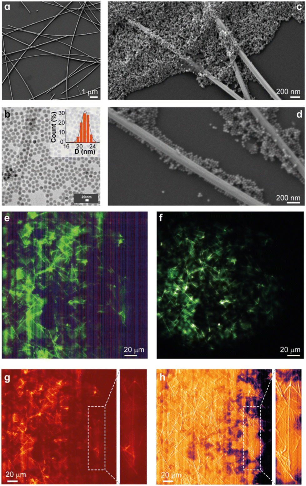 | ||
| Fig. 1 (a) SEM image of AgNWs deposited on silicon wafer, (b) TEM image of UCNPs. Inset: particle size distribution. The solid line is a fit of a normal distribution. (c and d) SEM image of AgNWs on glass coated with UCNPs by drop-casting. (e) HSM image. 50× magnification, applied voltage = 0 V, acquisition time = 250 ms. Laser power = 0.25(2) W cm−2. (f) Optical image under NIR (980 nm) light illumination. (g) Intensity map constructed from the integration of the UC spectra at each pixel showing enhanced emission intensity along the NWs. (h) Map of the signal-to-noise ratio calculated as described in the ESI.† The white-dashed contour highlights a single NW hardly seen in the intensity map but clearly exposed in the SNR map. | ||
2.1 Effects of AgNWs on the emission spectra of UCNPs
A raw image from the HSM performed on the sample and the corresponding photograph under 980 nm laser light illumination are shown in Fig. 1e and f, respectively. After processing the hyperspectral data for baseline correction and integration of each spectral band it was possible to construct a map of the total intensity (Fig. 1g) and the signal-to-noise ratio (Fig. 1h). Notably, the intensity map and the image under NIR illumination enable the direct visualization of the AgNW network because the emission intensity is higher at the positions of the AgNWs, pointing at an enhancement effect that cannot be attributed to a higher concentration of UCNPs. Interestingly, the SNR map shows an image of great detail of the AgNW network. Compared to the intensity map, the SNR map resolves with higher definition the presence of AgNWs and crossing points. See for example the NW highlighted in the white contour in Fig. 1g and h. Although this is not the focus of the current work, the artificial texture observed through the SNR processing may be of interest for other systems and nanostructures.A closer look at the HSM images allows us to compare the emission spectra at different locations within the AgNW network. In Fig. 2a, a collection of points of interest is highlighted within the intensity map where the color scale indicates a higher intensity over the AgNWs. We selected for comparison points located over junctions of AgNWs (P1, P3, P5 and P7), or at certain distances (P2, P4, P6 and P8). The corresponding normalized spectra at each location are shown in Fig. 2b. The spectra colored in gray fall below the cut-off criterion adopted to discard data points with low SNR spectra (see the Materials and methods section). The most important feature to notice is the intensity of the 2H9/2 → 4I13/2 band (IH9/2), observed as a peak centered at 558 nm. The height of this peak is different in each point, being higher at points located on AgNW junctions, e.g. P1, P3 and P5. We can construct a map of the relative weight of the 2H9/2 → 4I13/2 band by plotting the ratio between the intensity IH9/2 and the total intensity of the full spectra. This is shown in Fig. 2c where the red-colored regions represent the highest values and are mostly (although not exclusively) located at junctions between AgNWs. The values of intensity and other parameters of interest for the selected points are tabulated in Table S1, ESI.†
 | ||
| Fig. 2 (a) Selected region of the intensity map and points of interest within the AgNW network. (b) Emission spectra corresponding to the locations indicated in (a). (c) Map of the relative intensity of the 2H9/2 → 4I13/2 transition calculated as the ratio of the integrated spectra between 555 nm and 565 nm and the integration of the full spectra. (d) Schematic energy diagram of the 4fn multilevel structure involved in energy transfer upconversion. Solid arrows indicate absorption or emission of photons, dashed arrows indicate transitions between energy levels and curved arrows represent non-radiative relaxations. | ||
The optical transition behind the 2H9/2 → 4I13/2 band involves a three-photon process in which the energy transfer from Yb3+ to Er3+ occurs in three successive steps (energy scheme in Fig. 2d). As the probability of such transition is low, the spectral intensity of this emission becomes relevant at increasing excitation power. The map shown in Fig. 2c points out a local enhancement of the excitation light, an effect that is well known to occur in plasmonic nanoparticles at specific locations where the electric field is enhanced, commonly referred to as hot-spots. Both the plasmonic effect in individual AgNWs and the observation of hot-spots in AgNW networks have been reported by several groups.15,22,34,35 It is worth mentioning that other non-linear optical processes can also be mediated by plasmonic enhancement, for example, the simultaneous absorption of photons with energy lower than that of a semiconductor band gap.36
In Fig. 3 we analyze in greater detail the enhancement across a set of lines crossing different regions of interest, for example, across individual AgNWs (A, B, D, and F) and junctions between two or more wires (C and E). Fig. 3a shows the location of the selected regions on the total intensity map, while Fig. 3b presents the corresponding line profiles. A simple evaluation of the intensity enhancement factor (IEF) was calculated as  , where Imax is the peak maximum intensity and Ibkg is the background value, i.e., far away from the AgNWs. It can be seen that the enhancement factor across a single AgNW is on the order of 2 to 5, while across junctions the IEF is higher, e.g., 7.6 (E) and reaches as much as 15.7 (C). The enhancement is not homogeneous due to several factors including the inhomogeneous covering with UCNPs, the profile of the excitation light beam, the intrinsic features of the hyperspectral camera, and the constructive or destructive interference of electric fields generated by the NWs that affect distinctly the UCNPs situated in the interstitial regions.37 Although the enhancement is not uniform, the pixels at the junctions generally exhibit greater intensity than their surroundings. The color scale in Fig. 3a highlights these points of higher intensity, making them stand out, while less intense areas remain less noticeable. To provide a clearer view, Fig. S10 (ESI†) presents a detailed analysis with close-up cutouts of Fig. 3a, where the color scale was adjusted to maximize the contrast in each area.
 | ||
| Fig. 3 Analysis of the intensity enhancement factor (IEF) across the AgNW network. (a) Selected region of interest in the total intensity map for the analysis of the line profiles (blue lines). (b) Intensity profiles at selected regions and calculated IEF. | ||
Fig. 4a shows a comparison of the profiles for the normalized total intensity and IH9/2. The spatial extent of the enhancement effect across a single AgNW (A, Fig. 3a) and at a multiple junction cross-point (C, Fig. 3a) is presented in Fig. 4b. The characteristic lengths of the enhancement effect were calculated as the decay constant from fitting exponential growth/decay curves. From the analysis of multiple line profiles, we obtain a decay length of 1.0(6) μm.
 | ||
| Fig. 4 (a) Comparison of normalized intensity profiles across line A (Fig. 3a). (b) Comparison of profiles of IH9/2 across lines A (single AgNW, Fig. 3a) and C (multiple junctions, Fig. 3a). Dashed lines are exponential fitting curves for the calculation of the characteristic length of the enhancement effect. (c–e) Scanning luminescence thermometry conducted on a glass sample with a deposit of AgNWs on half of its surface. A drop of UCNP colloid was applied on top. The surface was scanned with a step size of 30 μm in a 3.0 mm × 1.5 mm window containing the boundary between regions with and without AgNWs at the border of the UCNP drop. (c) Schematic of the sample prepared for scanning. (d) Total intensity of the emission spectra. (e) Relative weight of the 2H9/2 → 4I13/2 transition. | ||
The enhancement effect is interesting as a possible strategy to boost the luminescence of UCNPs. A wide variety of plasmonic nanostructures have been explored for this purpose in the past. Here, we show that HSM allows for a direct visualization of the hot-spots and a quantitative measurement of the enhancement profiles. Nevertheless, an independent confirmation of the enhancement effect in AgNW networks is essential as a control measurement. For that, we performed scanning luminescence thermometry using an experimental setup that allows the scanning of a surface with a focused NIR laser light while recording the UCL. A detailed description of the method can be found elsewhere.38 We applied this technique to scan a glass substrate that was half-covered with AgNWs and fully covered with UCNPs in a window comprising the boundary between regions with and without AgNWs. The collected spectral results with this scanning were processed to obtain the total emission intensity, and the relative weight of the 2H9/2 → 4I13/2 band compared to the total intensity. The results are shown in Fig. 4(c–e) and confirm the two main conclusions observed in the HSM analysis: (i) the higher total intensity, and (ii) the higher relative intensity of the 2H9/2 → 4I13/2 band in the region with AgNWs. Fig. S7 (ESI†) shows the non-corrected thermometric parameter to be discussed in a later section.
Control experiments on UCNPs without AgNWs revealed an increased relative intensity of the 2H9/2 → 4I13/2 transition with higher excitation laser power. This observation mirrors the behavior observed in the presence of AgNWs, supporting our hypothesis that surface plasmon modes in each AgNW mix at the junctions to yield hybridized plasmon states presenting high local electromagnetic field values.34,39,40 These results are illustrated in Fig. S9 of the ESI.†
2.2 Calculation of the enhancement factor and the energy transfer rates
Metal-supported surface plasmons exhibit high polarizability. When they resonate with incident fields, this polarizability can induce extremely high-gradient fields, resulting in local field enhancement.41–43 This enhancement, induced by surface plasmons, may increase the rates involved in the photophysical properties of nearby UCNPs, such as absorption, energy transfer, and spontaneous emission coefficients. Specifically, we will quantitatively demonstrate how the local field enhancement, induced by the presence of a metallic nanowire, affects the oscillator strengths (fosc, eqn (S9) and (S11), ESI†) of the Yb3+ 2F7/2 → 2F5/2 transition through the enhancement factor, Ef. Therefore, the UCL is augmented, as this local field enhancement may lead to higher populations of the Er3+ excited levels through non-radiative Yb3+–Er3+ energy transfer, facilitating the 3-photon UCL process, which is evident with the appearance of the Er3+ 2H9/2 → 4I13/2 transition (ca. 556 nm, Fig. 2) at very low values of power density (ca. 0.25 W cm−2). For comparison, in the absence of the local field enhancement effect on the UCNPs, this transition only starts to appear at high power densities (ca. 29 W cm−2), indicating its utility as a power sensor.44First, let us quantitatively illustrate how plasmon–photon coupling changes the absorption rate of the lanthanide donor (Yb3+) in an UCNP by increasing the Yb3+ 2F7/2 → 2F5/2 oscillator strength, which is on the order of 10−6, as estimated in the ESI (see discussions around eqn (S11)†). In close proximity to a silver nanowire, the Ef can be estimated according to recent developments as:41
| Ef = 1 + fgeofω, | (1) |
 | (2) |
 | (3) |
The fω value remains constant as it depends on fixed parameters determined by the material and measurement conditions, resulting in fω = 44.76. Conversely, fgeo varies based on the distance between the metallic surface and the UCNP. We will consider two scenarios: (1) when the UCNP is positioned very close to the nanowire surface with Rp = 20 nm and (2) when it is situated far away with Rp = 200 nm.
In situation 1, fgeo is approximately 618, resulting in a significant enhancement of Ef ≈ 2.77 × 10⁴. Regarding absorption, the oscillator strength of the Yb3+ 2F7/2 → 2F5/2 transition within the UCNP should increase. This is achieved by augmenting the dipole strength (Sed, eqn (S6)†) from its value of Sed = 4.6 × 10−39 esu2 cm2 for Ln3+ transitions50 to approximately Sed = 2.12 × 10⁻³⁵ esu2 cm2, which is comparable to a spin-allowed transition (S0 → S1 of organic molecules).51,52 In numerical terms, this translates to redefining the oscillator strength (fosc, eqn (S9)†) as an “enhanced oscillator strength” (fposc) in the presence of the plasmonic effect as:
 | (4) |
| fposc ≈ fosc·Ef. | (5) |
Based on the value presented in eqn (S11),† the enhancement factor yields an fposc value of 0.1 for the 2F7/2 → 2F5/2 transition, which is comparable to the absorption of moderately conjugated systems like ketones.53
When the UCNP is located far from the plasmon-induced field, as described in situation 2, the value of fω remains constant at 44.76, while fgeo decreases significantly to 6.18 × 10⁻⁴. This decline nullifies the plasmonic effect, as the product fω·fgeo becomes 2.8 × 10⁻². Consequently, the enhancement factor approaches a value of 1 (Ef ≈ 1.02), indicating that the UCNP is practically unaffected by the plasmon-induced field anymore.
The calculations presented here take into account the interaction between a single UCNP–AgNW pair. Most importantly, they consider only the absorption of Yb3+. Er3+ emissions are proportional to the population of the Yb3+ excited state, which the model predicts will increase due to the increase in the local field. However, in the UCL process, the final emission intensity from Er3+ ions will not increase by a factor of EF because of the various energy transfer steps involved, each having intrinsic losses. So, it is expected that the intensity enhancement observed for emissions (IEF) will be much lower than the EF calculated for the absorption (given by the change in oscillator strength) of Yb3+.
Some additional points are worth mentioning, first, that the presence of a higher density of UCNP in the medium will lead to lower experimental EF values due to interference. So, the model is ideal for a more dilute system. Second, that the PVP native layer, forming a ca. 2 nm thick polymer coating around NWs, was not considered in the calculations. Lastly, that at NW junctions, the expected effect would be similar to that of an UCNP in a metallic nanocavity.54,55 This could further increase the EF (which would need to be modeled appropriately). Beyond these simplifications, the model adequately addresses the plasmonic interaction and the intensification observed in the hyperspectral images, in agreement with previous reports.
2.3 Effects on ratiometric thermometry
The relative weight of the 2H9/2 → 4I13/2 transition becomes relevant for the ratiometric determination of the thermometric parameter Δ. As stated in the Materials and methods section and described in a substantial number of published works,32,56–58Δ can be defined from the ratio between the integrated intensity of the 2H11/2 → 4I15/2 and 4S3/2 → 4I15/2 transitions, hereafter named IH and IS, respectively. However, the appearance of the 2H9/2 → 4I13/2 band constitutes an artifact in this simple processing because it partially overlaps with the 4S3/2 → 4I15/2 band affecting the calculation of IS. Correction algorithms must be applied to overcome this effect, for example, by deconvolution of the multi-peak spectra,44via a wavelength-resolved power-law study,57 or by cut-off integration38 to avoid the intrusive peak. Here, we proceed with the last method by first integrating IS up to 565 nm (we refer to this procedure as full integration, FI), and then subtracting IH9/2 from IS. Note that this is equivalent to a partial integration (PI) of the IS band up to 555 nm. In accordance with this strategy, a calibration procedure of the UCNPs was performed at varying temperatures (Fig. S4, ESI†). In Fig. 5 we compare the results of both methods of analysis in the construction of thermographic maps from measurements obtained at varying applied voltages on the AgNW network. The comparison of both methods is shown in the temperature maps of Fig. 5a–d. It can be seen that the full-integration method, i.e. using Δ = IH/IS, gives rise to an apparent thermal gradient near the AgNWs, where temperature readings on the AgNWs are slightly under that of the background. As heat is generated by the Joule effect due to the electric current conducted through the AgNW network, there is no physical explanation for the observation of lower temperatures on the AgNWs; therefore, an experimental artifact must be in play. Indeed, we find that the apparent lower temperatures on the AgNWs are related to the increased relative weight of IH9/2 in the emission spectra of UCNPs located in close proximity to the AgNWs, especially at junctions within the network. If the partial integration method is applied, i.e. subtracting IH9/2 from IS in the calculation of the thermometric parameter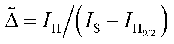 , then the apparent temperature gradient is strongly reduced or even disappears. In Fig. 5e, histograms of the temperature readings in the completed temperature maps under different applied voltages show a distribution that can be well modeled by a Gaussian peak. Mean temperatures are shown in Fig. 5f. There are two aspects worth mentioning: one is that with increasing applied voltages, the stationary temperature attainable is higher; the other is that the data obtained by the partial integration method are shifted to higher temperatures and show a lower standard deviation compared to the full-integration calculation. This is the result of the improvement in the determination of temperatures as artificial low-value readings are avoided. Data obtained from this analysis are summarized in Table 1.
 | ||
| Fig. 5 (a–d) Temperature maps constructed by ratiometric analysis considering the IS intensity as the full integration (FI) between 535 nm and 580 nm (left panels), and corrected temperature maps using the partial integration (PI) of the 4S3/2 → 4I15/2 transition from 535 nm to 555 nm (right panels). Scale bars are 5 μm. (e) Statistical analysis of temperatures readings at increasing applied voltages. (f) Comparison of the FI and PI integration methods for determining temperature distribution at increasing applied voltages. | ||
| Voltage (V) | Current (A) | Power (mW) | 〈TFI〉 (K) | σ FI (K) | 〈TPI〉 (K) | σ PI (K) | I H9/2/ITotal |
|---|---|---|---|---|---|---|---|
| 0 | 0 | 0 | 288.0 | 4.0 | 297.1 | 3.6 | 0.0962 |
| 2 | 40 | 80 | 297.4 | 4.6 | 302.0 | 4.0 | 0.0921 |
| 4 | 80 | 320 | 313.5 | 4.6 | 318.5 | 4.1 | 0.0871 |
| 6 | 120 | 720 | 337.1 | 4.7 | 342.8 | 4.0 | 0.0788 |
High values of IH9/2 represent an artifact in the temperature reading produced by a local enhancement of the NIR excitation light at junctions of NWs. We quantitatively analyzed this effect and the role of temperature by plotting the relative intensity of the 2H9/2 → 4I13/2 transition, defined as the intensity IH9/2 divided by the integration of the full spectra (ITotal), at different applied voltages. Fig. 6(a–d) show the maps of relative IH9/2 weight in a selected region of the HSM images. It can be seen that the contrast in the relative intensity IH9/2/ITotal gets diminished at higher temperatures, meaning that the enhancement effect is reduced with temperature, which is consistent with a plasmonic interaction.35 Statistical data and analysis of the constructed maps are shown in Fig. 6e, where the distribution of the relative weight IH9/2/ITotal shifts to lower values at increasing temperatures while the standard deviation is reduced. Fig. 6f shows the trend of the mean temperature values where the standard deviation is plotted as error bars.
 | ||
| Fig. 6 (a–d) Maps showing the relative intensity of the 2H9/2 → 4I13/2 transition in a selected region of the HSM images at increasing applied voltages. Corresponding mean temperatures are 297.1 K, 302.0 K, 318.5 K and 342.8 K, respectively. Scale bars are 5 μm. (e) Statistical analysis of the constructed maps. (f) Mean values of the relative intensity of the 2H9/2 → 4I13/2 transition. The standard deviations are plotted as error bars. | ||
Further analysis of the line profiles was focused on the effect of temperature, comparing the profiles from HSM images obtained at 0 V and 6 V applied voltages. This is shown in Fig. S6 (ESI†) where a minor reduction in the maximum intensity is observed at higher temperatures.
Lastly, we applied the HSM technique to dynamically measure the temperature evolution during heating and cooling experiments where we modified the voltage applied to the sample while running the acquisition of a hyperspectral image. In Fig. 7a we start with a sample at room temperature and 0 V applied. When the scanning is up to 200 lines we applied 3 V, and increased the voltage to 6 V after scanning 200 extra lines. In Fig. 7b we reverse the order of the applied voltage starting with 6 V, then 3 V and finally 0 V. In each case, we can observe the heating or cooling directly from the temperature maps constructed using the partial integration method. The profiles across a single column (highlighted as a white-dashed line) are shown in Fig. 7c (heating) and Fig. 7d (cooling). For increasing temperatures we found a maximum temperature slope of 1.9(2) K μm−1. Considering that the mean scan time per line is 3.4 s, we can calculate the time profile and the slope dT/dt = 0.56(5) K s−1. Using the time resolution given by56
 | (6) |
 | ||
| Fig. 7 Dynamic HSM imaging under varying applied external voltages. Temperature maps obtained by the partial integration method of in situ HSM imaging under (a) increasing and (b) decreasing applied voltages. Scale bars are 15 μm. Temperature profiles across the column highlighted with a white-dashed line for (c) increasing and (d) decreasing applied voltages. | ||
3 Conclusions
In this work, we applied HSM in combination with Er3+-doped UCNPs to map the temperature profile across a network of silver nanowires. We found that upon excitation with NIR 980 nm laser light, small-size UCNPs deposited over the AgNW network reveal spatial locations with increased emission intensity. These regions are located across AgNWs with particularly intense emission on UCNPs located in the cross-point junctions of AgNWs, pointing at the location of hot-spots where the enhancement of UCL is more intense. Furthermore, we show that the emission spectra are modified in close proximity (<1 μm) to AgNWs presenting a higher intensity of the 2H9/2 → 4I13/2 transition, which is associated with a three-photon absorption process. This effect reveals a higher local intensity of the electric field and an increased absorption rate of Yb3+, in agreement with numerical calculations and previously reported plasmonic effects. The presence of the 2H9/2 → 4I13/2 transition introduces an artifact in the determination of the temperature using conventional ratiometric methods leading to false low-temperature readings on the AgNWs. A correction method was implemented to reduce this effect in order to consistently map the temperatures under different electrical powers applied to the AgNW network. We highlight the importance of HSM to directly visualize plasmonic effects on luminescence and the location of hot-spots. At the same time, optical thermometry based on UCNPs was improved by considering the effect of the nanostructure in the emission spectra. We consider these two topics as relevant for the study of thermal and plasmonic effects on other nanostructures and nanomaterials.4 Materials and methods
4.1 Preparation of samples
To analyze the heat dissipation in AgNWs we prepared a set of samples comprising a percolated network of AgNWs coated with UCNPs. The synthesis of UCNPs was carried out using the co-precipitation route.59 In this process, precursor materials were carefully combined under controlled conditions to yield β-NaY0.78F4:Yb0.2:Er0.02 UCNPs with the desired properties. The synthesis of AgNWs was achieved through the polyol method, involving the reduction of silver ions in the presence of polyvinylpyrrolidone (PVP) in ethylene glycol.60 AgNWs were used to formulate a stable colloid in a mixture of 2-propanol and water with the addition of sodium poly(stryrene sulfonate) (PSS).61 On clean glass slides, a coating with AgNWs was formed by spin coating at 3000 rpm followed by drying at 60 °C on a heating plate. Electrical contacts were made on opposite sides of the AgNW networks using a silver conductive paint. UCNPs were deposited on top of the AgNW networks by drop casting 10 μL of a cyclohexane colloid. Detailed procedures and conditions for both syntheses are elaborated in the ESI.† A calibration procedure for the use of UCNPs as thermal probes was performed by measuring the emission spectra of UCNPs on a heating plate at known temperatures from 293 K to 353 K.25 A reference thermometer (RTD Pt100) was used in thermal contact by means of a high-thermal conductivity paste, and the temperature was set with a precision of ±0.2 K using a temperature controller (Novus N321-Pt100). The results of the calibration are shown in Fig. S4, ESI.†4.2 Hyperspectral microscopy (HSM)
HSM was performed using a CytoViva system equipped with an Olympus BX51 microscope. The system was used for the visualization of the samples under bright field (BF) and dark field (DF) illumination. An additional port of the microscope light entrance was used to illuminate the sample with 980 nm laser light. A 50× objective lens and a positional mirror were used to deflect the light to any of the two digital cameras available: a CCD camera (Retiga 4000 R, QImaging) for optical image acquisition, and a visible and near-infrared (VNIR) spectrophotometer with an integrated camera for the acquisition of the emission spectra at each point in the field of view. The CytoViva hyperspectral line-scanning imaging system is constituted by a digital camera (IPX-2M30, Imperx) coupled to a spectrograph (V10E 2/3 inch, Specim, with a 30 μm slit, a nominal spectral range of 400–1000 nm, and nominal spectral resolution of 2.73 nm).The described samples were affixed to the stage of the optical microscope and connected for electrothermal stimulation using a DC power source. A digital multimeter was connected in series to measure the current. Initially, an image of the sample was captured in dark field (DF) mode. Subsequently, an image was acquired with the exclusive illumination from a 980 nm laser, 0.25(2) W cm−2, focused on the sample with a field of view of approximately 200 μm in diameter.62 A hyperspectral image was obtained under the same illumination conditions, configuring the spectral bands for acquisition to cover the luminescence range from 500 nm to 580 nm with a 1.24 nm spectral resolution, incorporating a total of 66 spectral bands. The nominal resolution of the spectrometer (2.73 nm) refers to the spectrometer's ability to distinguish between two closely spaced spectral lines or features. This value, often determined at the FWHM of a peak, indicates the minimum spectral separation at which the instrument can resolve two peaks as distinct entities. On the other hand, the wavelength step at which the spectrograph records each emission spectrum (1.24 nm) is dependent on the range of wavelengths the spectrometer is configured to record and the number of pixels available in the detector, and so is determined by the settings of the instrument. The constructed hyperspectral image comprises 696 × 696 pixels2, recorded line-by-line in a dark-controlled environment, with a total acquisition time per image of approximately 40 minutes. HSM can achieve high spatial resolution as each pixel field-of-view recorded with a 100× objective corresponds to 129 × 129 nm2, so the pixel size can be as low as 129 × 129 nm2.62 In contrast, confocal techniques can achieve higher spatial resolution by focusing the excitation light below 1 μm,30 limited by diffraction. Additionally, the positioning platform can achieve remarkable precision (below 10 nm) using piezoelectric stages, enabling images with a pixel size of 10 × 10 nm2. However, the resolving power of the imaging technique is ultimately constrained by the spot size.
4.3 Image processing
Following image acquisition, hyperspectral data underwent processing to generate maps depicting emission intensity, thermometric parameters, and signal-to-noise ratio (SNR). First, a baseline correction was performed for each image by subtracting a linear baseline fit from the off-emission wavelengths of Er3+. These wavelengths encompassed data points from 500 nm to 515 nm and from 565 nm to 580 nm (Fig. S5, ESI†). Subsequently, the intensity of emission bands was determined by integrating spectra from 515 nm to 534 nm and from 534 nm to 565 nm, respectively, corresponding to the IH (2H11/2 → 4I15/2) and IS (4S3/2 → 4I15/2) transitions. The total emission intensity resulted from the summation of both bands, while the conventional thermometric parameter Δ was computed as the ratio between them as . To mitigate unrealistic values from low-intensity pixels, a cut-off criterion was applied, setting IH to zero if its value fell below a specified threshold. Alternatively, we define a different thermometric parameter in order to avoid the interference of the three photon radiative transition 2H9/2 → 4I13/2 whose integrated intensity is named here as IH9/2 and results from the integration from 555 nm to 565 nm. The new thermometric parameter is defined as
  where IScut results from the integration from 534 nm to 555 nm.
4.4 Ratiometric thermometry
The relationship between the thermometric parameter and the temperature lies in the thermally coupled populations of the 2H11/2 and 4S3/2 levels following the Boltzmann law. Using a known reference temperature (T0) and the corresponding thermometric parameter (Δ0), temperatures can be calculated from the emission spectra using:44,56,63,64 | (7) |
Data availability
The data supporting this article have been included as part of the ESI.†Conflicts of interest
There are no conflicts to declare.Acknowledgements
The authors thank Prof. Carlos Rettori (UNICAMP) and Prof. Ricardo R. Urbano (UNICAMP) for their support in the realization of this work. We thank Dr C. Bertoli (CAB-CNEA) for images obtained in SEM. TEM images were acquired at LNNano, Centro Nacional de Pesquisa em Energia e Materiais (CNPEM) in Campinas-SP, Brazil. This work was supported by ANPCyT-FONCyT PICT 2020-0697 and from the CAPES PrInt fellowship #88887.716554/2022-00 in which L. H. A. R. F. received an exchange scholarship during his doctorate. E. D. M. was the beneficiary of a post-doctoral FAPESP fellowship #2015/23882-4 and BEPE #2018/12489-8 during part of the development of this work. This work is also developed within the scope of the projects at CICECO-Aveiro Institute of Materials, UIDB/50011/2020 (https://doi.org/10.54499/UIDB/50011/2020), UIDP/50011/2020 (https://doi.org/10.54499/UIDP/50011/2020) & LA/P/0006/2020 (https://doi.org/10.54499/LA/P/0006/2020) financed by Portuguese funds through the FCT/MCTES (PIDDAC). This work was initiated at IFGW-UNICAMP, Brazil, and finished at the current affiliation of the corresponding author.Notes and references
- J. Zhou, Q. Liu, W. Feng, Y. Sun and F. Li, Chem. Rev., 2015, 115, 395–465 CrossRef CAS PubMed.
- B. Chen and F. Wang, Trends Chem., 2020, 2, 427–439 CrossRef CAS.
- G. Chen, H. Qiu, P. N. Prasad and X. Chen, Chem. Rev., 2014, 114, 5161–5214 CrossRef CAS PubMed.
- T. Liu, X. Liu, Y. Feng and C.-J. Yao, Mater. Today Chem., 2023, 34, 101788 CrossRef CAS.
- D. Lu, S. K. Cho, S. Ahn, L. Brun, C. J. Summers and W. Park, ACS Nano, 2014, 8, 7780–7792 CrossRef CAS.
- J. Dong, W. Gao, Q. Han, Y. Wang, J. Qi, X. Yan and M. Sun, Rev. Phys., 2019, 4, 100026 CrossRef.
- W. Park, D. Lu and S. Ahn, Chem. Soc. Rev., 2015, 44, 2940–2962 RSC.
- E. Martínez, A. Prado, M. González, S. Anguiano, L. Tosi, L. S. Alarcón and H. Pastoriza, J. Lumin., 2021, 233, 117870 CrossRef.
- Y. Xue, C. Ding, Y. Rong, Q. Ma, C. Pan, E. Wu, B. Wu and H. Zeng, Small, 2017, 13, 1–11 Search PubMed.
- A. L. Feng, M. L. You, L. Tian, S. Singamaneni, M. Liu, Z. Duan, T. J. Lu, F. Xu and M. Lin, Sci. Rep., 2015, 5, 1–10 Search PubMed.
- M. Saboktakin, X. Ye, S. J. Oh, S. H. Hong, A. T. Fafarman, U. K. Chettiar, N. Engheta, C. B. Murray and C. R. Kagan, ACS Nano, 2012, 6, 8758–8766 CrossRef CAS PubMed.
- W. Luo, F. Xu, A. Li and Z. Sun, Adv. Opt. Mater., 2022, 10, 1–10 Search PubMed.
- A. Chu, H. He, Z. Yin, R. Peng, H. Yang, X. Gao, D. Luo, R. Chen, G. Xing and Y. J. Liu, ACS Appl. Mater. Interfaces, 2020, 12, 1292–1298 CrossRef CAS.
- H. Mertens and A. Polman, Appl. Phys. Lett., 2006, 89, 211107 CrossRef.
- K. Park, K. Jung, S. J. Kwon, H. S. Jang, D. Byun, I. K. Han and H. Ko, Adv. Funct. Mater., 2016, 26, 7836–7846 CrossRef CAS.
- W. Xu, T. K. Lee, B. S. Moon, H. Song, X. Chen, B. Chun, Y. J. Kim, S. K. Kwak, P. Chen and D. H. Kim, Adv. Opt. Mater., 2018, 6, 1–11 Search PubMed.
- W. Feng, L. D. Sun and C. H. Yan, Chem. Commun., 2009, 4393–4395 RSC.
- K. Wiwatowski, K. Sulowska, R. Houssaini, A. Pilch-Wróbel, A. Bednarkiewicz, A. Hartschuh, S. Maćkowski and D. Piątkowski, Nanoscale, 2023, 15, 10614–10622 RSC.
- A. Borodziuk, K. Sulowska, Ł. Zinkiewicz, M. Szymura, A. Reszka, A. Bogucki, B. Sikora, S. Maćkowski and Ł. Kłopotowski, J. Phys. Chem. C, 2022, 126, 19219–19228 CrossRef CAS.
- A. Prymaczek, M. Cwierzona, J. Grzelak, D. Kowalska, M. Nyk, S. Mackowski and D. Piatkowski, Nanoscale, 2018, 10, 12841–12847 RSC.
- A. Prymaczek, M. Cwierzona, M. A. Antoniak, M. Nyk, S. Mackowski and D. Piatkowski, Sci. Rep., 2021, 11, 1–8 CrossRef PubMed.
- D. Piatkowski, N. Hartmann, T. MacAbelli, M. Nyk, S. MacKowski and A. Hartschuh, Nanoscale, 2015, 7, 1479–1484 RSC.
- H. Wei, D. Ratchford, X. Li, H. Xu and C. K. Shih, Nano Lett., 2009, 9, 4168–4171 CrossRef CAS.
- D. Buczyńska, M. Ćwik, E. Roźniecka, K. Sulowska, D. Piatkowski, S. Maćkowski and J. Niedziółka-Jönsson, J. Phys. Chem. C, 2020, 124, 15418–15424 CrossRef.
- E. D. Martínez, A. F. García Flores, H. Pastoriza, R. R. Urbano and C. Rettori, Sens. Actuators, B, 2018, 259, 475–483 CrossRef.
- E. D. Martínez, C. D. S. Brites, L. D. Carlos, A. F. García-Flores, R. R. Urbano and C. Rettori, Adv. Funct. Mater., 2019, 29, 1807758 CrossRef.
- M. Suta and A. Meijerink, Adv. Theory Simul., 2020, 3, 2000176 CrossRef CAS.
- C. D. Brites, A. Millán and L. D. Carlos, Handbook on the Physics and Chemistry of Rare Earths, 2016, vol. 49, pp. 339–427 Search PubMed.
- C. D. S. Brites, R. Marin, M. Suta, A. N. Carneiro Neto, E. Ximendes, D. Jaque and L. D. Carlos, Adv. Mater., 2023, 2302749, 1–45 Search PubMed.
- T. P. Van Swieten, T. Van Omme, D. J. Van Den Heuvel, S. J. Vonk, R. G. Spruit, F. Meirer, H. H. P. Garza, B. M. Weckhuysen, A. Meijerink, F. T. Rabouw and R. G. Geitenbeek, ACS Appl. Nano Mater., 2021, 4, 4208–4215 CrossRef CAS PubMed.
- E. D. Martínez, C. D. Brites, R. R. Urbano, C. Rettori and L. D. Carlos, Phys. B, 2022, 629, 413639 CrossRef.
- J. C. Martins, A. R. N. Bastos, R. A. S. Ferreira, X. Wang, G. Chen and L. D. Carlos, Adv. Photonics Res., 2021, 2, 2000169 CrossRef CAS.
- S. J. W. Vonk, T. P. van Swieten, A. Cocina and F. T. Rabouw, Nano Lett., 2023, 23, 6560–6566 CrossRef CAS PubMed.
- Z. Bi, M. Yang, Y. Shang, X. Meng, H. Zhang and G. Shang, Opt. Commun., 2018, 429, 35–40 CrossRef CAS.
- M. Razeghi, M. Üstünçelik, F. Shabani, H. V. Demir and T. S. Kasırga, Nanoscale Horiz., 2022, 7, 396–402 RSC.
- H. Siampour and Y. Dan, Opt. Express, 2016, 24, 4601 CrossRef CAS PubMed.
- J. He, W. Zheng, F. Ligmajer, C. F. Chan, Z. Bao, K. L. Wong, X. Chen, J. Hao, J. Dai, S. F. Yu and D. Y. Lei, Light: Sci. Appl., 2017, 6, e16217 CrossRef CAS PubMed.
- A. M. Aguilar, E. L. Saidman, M. V. Rosato-Siri, L. Marpegán and E. D. Martínez, ACS Appl. Nano Mater., 2023, 6, 20942–20953 CrossRef CAS.
- T. Kang, I. Yoon, K. S. Jeon, W. Choi, Y. Lee, K. Seo, Y. Yoo, Q. H. Park, H. Ihee, Y. D. Suh and B. Kim, J. Phys. Chem. C, 2009, 113, 7492–7496 CrossRef CAS.
- R. Chikkaraddy, D. Singh and G. V. Kumar, Appl. Phys. Lett., 2012, 100, 1–4 CrossRef.
- X. Qin, A. N. Carneiro Neto, R. L. Longo, Y. Wu, O. L. Malta and X. Liu, J. Phys. Chem. Lett., 2021, 12, 1520–1541 CrossRef CAS PubMed.
- A. N. Carneiro Neto, M. A. Couto dos Santos, O. L. Malta and R. Reisfeld, Metal Nanostructures for Photonics, Elsevier, 2019, pp. 19–36 Search PubMed.
- E. C. Le Ru and B. Auguié, ACS Nano, 2024, 18, 9773–9783 CrossRef CAS PubMed.
- J. C. Martins, A. Skripka, C. D. S. Brites, A. Benayas, R. A. S. Ferreira, F. Vetrone and L. D. Carlos, Front. Photonics, 2022, 3, 1–10 Search PubMed.
- M. Couto dos Santos, O. Malta and R. Reisfeld, J. Lumin., 2016, 170, 271–274 CrossRef CAS.
- B. Persson and A. Liebsch, Solid State Commun., 1982, 44, 1637–1640 CrossRef CAS.
- L. Bányai and P. Gartner, Phys. Rev. B: Condens. Matter Mater. Phys., 1984, 29, 728–734 CrossRef.
- C. Noguez and C. E. Román-Velázquez, Phys. Rev. B: Condens. Matter Mater. Phys., 2004, 70, 195412 CrossRef.
- M. G. Blaber, M. D. Arnold and M. J. Ford, J. Phys. Chem. C, 2009, 113, 3041–3045 CrossRef CAS.
- A. Ćirić, T. Gavrilović and M. D. Dramićanin, Crystals, 2021, 11, 189 CrossRef.
- P. A. Tanner, W. Thor, Y. Zhang and K.-L. Wong, J. Phys. Chem. A, 2022, 126, 7418–7431 CrossRef CAS PubMed.
- A. N. Carneiro Neto, R. T. Moura, L. D. Carlos, O. L. Malta, M. Sanadar, A. Melchior, E. Kraka, S. Ruggieri, M. Bettinelli and F. Piccinelli, Inorg. Chem., 2022, 61, 16333–16346 CrossRef CAS.
- M. F. Vansco, B. Marchetti and M. I. Lester, J. Chem. Phys., 2018, 149, 244309 CrossRef.
- Y. Wu, J. Xu, E. T. Poh, L. Liang, H. Liu, J. K. Yang, C. W. Qiu, R. A. Vallée and X. Liu, Nat. Nanotechnol., 2019, 14, 1110–1115 CrossRef CAS PubMed.
- Y. Meng, D. Huang, H. Li, X. Feng, F. Li, Q. Liang, T. Ma, J. Han, J. Tang, G. Chen and X.-W. Chen, Nat. Photonics, 2023, 17, 73–81 CrossRef CAS.
- C. Brites, A. Millán and L. Carlos, Handbook on the Physics and Chemistry of Rare Earths, Elsevier, 2016, vol. 49, pp. 339–427 Search PubMed.
- A. R. Pessoa, J. A. O. Galindo, L. F. dos Santos, R. R. Gonçalves, S. A. Maier, L. d. S. Menezes and A. M. Amaral, J. Phys. Chem. C, 2023, 127, 9673–9680 CrossRef CAS.
- J. A. Galindo, A. R. Pessoa, Y. E. Serge-Correales, S. J. Ribeiro, L. d. S. Menezes and A. M. Amaral, J. Lumin., 2023, 257, 119685 CrossRef CAS.
- F. Wang, R. Deng and X. Liu, Nat. Protoc., 2014, 9, 1634–1644 CrossRef CAS PubMed.
- J. Jiu, T. Araki, J. Wang, M. Nogi, T. Sugahara, S. Nagao, H. Koga, K. Suganuma, E. Nakazawa, M. Hara, H. Uchida and K. Shinozaki, J. Mater. Chem. A, 2014, 2, 6326–6330 RSC.
- J. I. Diaz Schneider, P. C. Angelomé, L. P. Granja, C. P. Quinteros, P. E. Levy and E. D. Martínez, Adv. Electron. Mater., 2022, 8, 2200631 CrossRef CAS.
- R. N. Silva, A. M. Botas, D. Brandão, V. Bastos, H. Oliveira, M. L. Debasu, R. A. Ferreira, C. D. Brites and L. D. Carlos, Phys. B, 2022, 626, 413470 CrossRef CAS.
- S. Balabhadra, M. L. Debasu, C. D. S. Brites, R. A. S. Ferreira and L. D. Carlos, J. Phys. Chem. C, 2017, 121, 13962–13968 CrossRef CAS.
- P. Rühl, D. Wang, F. Garwe, R. Müller, M. Haase, K. W. Krämer, W. Paa, R. Heintzmann, S. H. Heinemann and H. Stafast, J. Lumin., 2021, 232, 18–21 CrossRef.
Footnote |
| † Electronic supplementary information (ESI) available: Detailed description of the synthesis of UCNPs and AgNWs, HR-TEM image and XRD data of UCNPs, TEM images of AgNWs, additional SEM images and EDS of samples under study, data of thermal calibrations of UCNPs, baseline correction processing, table summarizing the results on selected points of interest, line profiles across AgNWs under 0 V and 6 V applied voltages and UV-visible spectra of AgNWs. See DOI: https://doi.org/10.1039/d4nr02484b |
| This journal is © The Royal Society of Chemistry 2024 |