
Enhanced photoelectrochemical and photocatalytic performance of iodine-doped titania nanotube arrays†
Katarzyna Siuzdak*a,
Mariusz Szkodab,
Mirosław Sawczaka,
Anna Lisowska-Oleksiakb,
Jakub Karczewskic and
Jacek Ryld
aCentre of Plasma and Laser Engineering, Szewalski Institute of Fluid-Flow Machinery, Polish Academy of Sciences, Fiszera 14, Gdańsk 80-231, Poland. E-mail: ksiuzdak@imp.gda.pl; Fax: +48 58 3416144; Tel: +48 58 6995294
bDepartment of Chemistry and Technology of Functional Materials, Chemical Faculty, Gdańsk University of Technology, Narutowicza 11/12, Gdańsk 80-233, Poland
cFaculty of Applied Physics and Mathematics, Gdańsk University of Technology, Narutowicza 11/12, 80-233 Gdańsk, Poland
dDepartment of Electrochemistry, Corrosion and Materials Engineering, Gdańsk University of Technology, Narutowicza 11/12, 80-233 Gdańsk, Poland
First published on 2nd June 2015
Abstract
The paper discusses the synthesis and performance of iodine doped titania nanotube arrays exhibited under irradiation. The doping procedure was performed as an additional, electrochemical process carried out after formation of nanotube arrays via anodization of the Ti substrate. The optical and structural properties were characterized using Raman, UV-vis, photoluminescence and X-ray photoelectron spectroscopy. The surface morphology and cross-section studies performed by means of scanning electron microscopy show that the ordered tubular architecture is not influenced by the doping method. However, iodine doping causes a reduction of bandgap energy and photoluminescence intensity. The nanotubular TiO2 electrodes have been monitored by electrochemical (using cyclic voltammetry and electrochemical impedance spectroscopy) and in situ UV-vis spectroelectrochemical measurements in contact with an aqueous electrolyte. Collected results show significant differences in electrochemical activity between pure and doped titania exhibited as i.e. change of Mott–Schottky relation or shift in the onset potential when a decrease in reflectance is initiated. The photocurrent density reached 155.2 and 142.2 μA cm−2 for iodine doped materials when KI and HIO4 were used as iodine precursors whereas only 25.6 μA cm−2 was registered for pure titania nanotubes under UV-vis illumination. Moreover, doped samples are far more efficient for the photodegradation progress than undoped material leading to decomposition of over 70% of methylene blue used as a model organic pollutant. The reported studies demonstrate for the first time the detailed optical, electrochemical and photoelectrochemical studies of iodine doped nanotube arrays.
A Introduction
Highly ordered titania nanotube arrays have attracted worldwide attention in different fields of science and industrial technology because of a significant number of potential applications enabled by the electric, ionic, absorbance and biomedical properties of nanotubes.1 In comparison to TiO2 nanoparticles, tubular architecture allows, e.g. for a non-disturbed charge transport along the tube wall and specific light capture inside the pores.2 Titania nanotubes possessing a large surface area, characterized by strong mechanical strength and perfect alignment are regarded as materials of great scientific and practical concern. Such nanostructures could be achieved using the anodization technique, known as one of the cheapest, straight-forward and simplest synthesis method resulting in the highly ordered material.3 Furthermore, the structure of titania nanotubes formed during the anodization process could be easily controlled by changing the anodization potential, temperature, and electrolyte composition or geometry of the electrolytic cell.4,5 Until now, layers composed of TiO2 nanotube arrays have been successfully used in dye-sensitized solar cells,6 gas sensors,7 as a photocatalyst8 or membrane for protein separation and drug delivery.9 However, nanotube activity in processes carried out under illumination is limited by their wide bandgap Ebg that corresponds to ultraviolet light.10 While the large Ebg is crucial for many applications, it limits the use of solar-irradiated driven applications, because only 5% of the total sun spectra are provided in the UV range. Therefore, different strategies were proposed in order to shift the activity of titania towards longer wavelengths. Bandgap engineering is mainly based on bulk doping or surface modification.11 Among them, non-metal doping is regarded as simple, providing material that is stable and highly active under visible light illumination. For intentional doping of titania nanotubes: nitrogen,12 sulfur,13 phosphorus,14 boron15 and iodine16 atoms were proposed as favorable non-metallic candidates. Taking into account the number of scientific reports, nitrogen and boron are the most popular dopant atoms and their presence in the structure of titania results in a highly active material, whereas studies on other possible non-metal dopant atoms are not widespread. Until now, no electrochemical investigation including registration of transient photocurrent under UV-vis illumination or impedance studies has been performed for the iodine doped TiO2.16,17 Such research enables a description of redox properties that are among the most important features of any functional material for solar energy utilization involving photocatalysis and photovoltaics. Depending on the crystal structure, particle size, doping level, surface modification, environment, titanium dioxide as with any other semiconducting material is characterized by unique potentials of band edges. Thus, in order to make a comprehensive characterization of the semiconductor, great effort should be made to ensure a proper determination of potentials of band edges. As it is known, in the absence of external filed, the interface of the semiconductor with an aqueous electrolyte solution is usually characterized by band bending caused by adjustment of the Fermi level with the corresponding energy level in solution.18 However, at a certain potential applied to the semiconducting electrode, the Fermi level lies at the same energy as the solution redox potential. There is no net transfer of charge and band bending does not occur.19 Such potential is described as flat-band potential (Efb) and because Efb for an n-type semiconductor lies at the vicinity of the conduction band (CB), the position of CB can be then estimated. Two different approaches are known that can be used for flat-band determination, referring to the excited or not-excited state of the semiconductor. In the first case, during the measurement, the sample is irradiated and in fact the potential of the quasi-Fermi level is determined that is useful for the photocatalytic processes.20–23 However, information about the redox properties of the semiconductor in its ground state can only be achieved without its light-driven excitation. Such conditions are met during electrochemical impedance spectroscopy and spectroelectrochemical measurements. In the case of pure and doped titanium dioxide nanotubes, the Mott–Schottky analysis of impedance data has already been used for flatband determination,24 whereas spectroelectrochemical measurements have been conducted only for semitransparent electrodes composed of thin layer of TiO2 nanoparticles.25–27 According to Świętek et al.,28 spectroelectrochemical determination of flat-band potential could be also successfully applied for non-transparent materials using diffuse reflectance spectroscopy combined together with electrochemical measurements. The tracking of changes in reflectance, that is strongly related to electron density in the conduction band, enables determination of the potential at which the electrochemical reduction of the semiconductor is initiated. However, until now this technique has not been used for the characterization of redox properties of titania nanotubes. Additionally, any comparison between two different approaches in determination of Efb position: (a) based on electrochemical impedance spectroscopy and (b) spectroelectrochemical measurement, to date has not been performed, analyzed and discussed.Here, we report preparation of iodine doped titanium dioxide nanotube arrays via electrochemical process carried out on biased as-anodized titania plates immersed in KI or HIO4 solution. Materials were characterized using various spectroscopic techniques: UV-vis, Raman, photoluminescence and X-ray photoelectron spectroscopy. Morphology, together with the elemental analysis, was studied using SEM equipped with EDX. The photocatalytic activity of nanotube array films was tested for the degradation of methylene blue as a model organic pollutant. A significant part of the research was focused on electrochemical characterization covering voltammetry as well as impedance measurements and spectroelectrochemical studies. Great attention has been paid to a discussion of flat-band potential determined using two different methods without exposition of studied material to simulated solar radiation: the first one based on electrochemical impedance spectroscopy and the second one based on an UV-vis spectroelectrochemical measurement. Moreover, the current response registered under both vis and UV-vis illumination for iodine doped titania was compared to that of pure TiO2 nanotubes.
B Experimental
Material preparation
Titania nanotubes were prepared via a two-step electrochemical anodization of analytical grade Ti plate (Steam, 99.7%) in a fluoride-containing solution. The procedure leading to formation of TiO2 nanotubes was described in our previous report.12 To sum it up briefly, it is based on a two-stage anodization process that provides highly ordered nanotubular architecture.5 The first and the second step were performed at the same temperature conditions (23 °C ± 1 °C), electrolyte composition (0.27 M NH4F in 1%/99% v/v water/ethylene glycol solution) and anodization parameters (40 V, 2 h). Before the second anodization, the nanotubular layer formed during the first step was removed by overnight etching in a 0.5% wt solution of oxalic acid. At the end of the entire anodization process, titanium plates covered with nanotubes were ultrasonically cleaned in 0.05% wt HF for 60 s, in order to remove surface debris.Iodine doping was realized similarly to Su et al.16 via an electrochemical process in a two-electrode arrangement in two types of electrolytes: 0.1 M solution of potassium iodide or periodic acid. When the periodic acid solution was used, the as-anodized titania nanotubes served as the cathode and a platinum mesh as the anode. On the contrary, when the solution of potassium iodide was applied as an electrolyte, the setting of Ti plate covered by TiO2 nanotubes and a platinum mesh were interchanged and they served as an anode and a cathode respectively. After optimization procedure, electrochemical doping was performed for 15 min at 1.5 V (23 °C ± 1 °C). According to the chemical formula of iodine precursors used, the titania nanotube samples were coded as: I–TiO2–KI and I–TiO2–HIO4. Finally, samples were rinsed with deionized water and annealed at a temperature of 450 °C for 2 h (heating rate: 2 °C min−1) in order to process conversion into the crystalline phase. Pure, ordered TiO2 nanotube arrays obtained after two-step anodization and a calcination process were used as a reference sample. Therefore, the only difference in the preparation procedure of pure and doped titania was the electrochemical doping step.
Characterization
The morphology and cross-section of the samples were investigated by the Schottky field emission scanning electron microscopy (FEI Quanta FEG 250) with ET secondary electron detector. Beam accelerating voltage was kept at 10 kV. For elemental analysis, the Energy Dispersive X-ray Spectroscopy was performed by EDAX Genesis APEX 2i with ApolloX SDD spectrometer in a particular area of each sample.The UV-vis reflectance spectra of titania nanotubes were measured with a dual beam UV-vis spectrophotometer (Lambda 35, Perkin-Elmer) equipped with a diffuse reflectance accessory. The spectra were registered in a range of 300–900 nm, with a scanning speed of 240 nm min−1. Bandgap energy values were determined as the intercept of the tangent of the plot of transformation of the Kubelka–Munk function (KM0.5Ef0.5) vs. photon energy, where KM = (1R)2/2R, R – the intensity of radiation reflected from the sample. This method is commonly used for both pure and doped titania nanotube arrays.
The Raman spectra were recorded by a confocal micro-Raman spectrometer (InVia, Renishaw) with sample excitation, by means of an argon ion laser emitting at 514 nm operating at 5% of its total power (50 mW).
The photoluminescence (PL) measurements were carried out using laboratory setup consisting of 0.3 m Czerny–Turner spectrograph (SR303i, Andor) equipped with ICCD camera (DH740, Andor). Samples of pure and doped TiO2 were excited with UV LED (365 nm center wavelength, 9 nm FWHM, 350 mW output power). The excitation radiation, focused by quartz lens, was directed onto the sample surface at an angle of 45°. Additionally, the band-pass filter (UG11, Schott) was applied between the excitation source and the sample to block UV LED radiation above 380 nm. The fluorescence signal was collected perpendicularly to the sample surface using a microscope objective and focused on the entrance of the optical fiber. In the detection path, the band-pass filters (GG44, Schott) were used for blocking the excitation radiation.
Escalab 250Xi from ThermoFisher Scientific was used to carry out high-resolution X-ray photoelectron spectroscopy (XPS) measurements to determine chemical binding properties of the surface, utilizing monochromatic Al Kα source with charge neutralization implemented by means of a flood gun. High-resolution spectra were recorded at energy step size of 0.1 eV at a pass energy of 10 eV. In order to normalize spectroscopic measurements, X axis (binding energy, Ebin) from XPS spectrum was calibrated for peak characteristics of neutral carbon 1 s (Ebin = 284.6 eV). Data analysis was performed using Avantage software provided by the manufacturer.
Electrochemical characterization
The electrochemical studies of pure and iodine-doped titania nanotubes (cyclic voltammetry: CV, linear sweep voltammetry LV, electrochemical impedance spectroscopy EIS) were conducted using an AutoLab PGStat 302N potentiostat–galvanostat system (Methrom, Autolab) in the standard three-electrode assembly, where titanium foil covered by nanotubes served as a working electrode (active surface area of 0.4 cm2). The Pt mesh was used as a counter electrode, while Ag/AgCl/0.1 M KCl as a reference electrode. All electrochemical tests were carried out in 0.1 M K2SO4 that was extensively purged with argon gas for about 1 h. Ar-cushion above the electrolyte was applied during the measurements.Electrochemical impedance spectroscopy measurements were conducted at the frequency range from 20 kHz to 0.1 Hz, covering 75 points and with 10 mV amplitude of the AC signal. In order to perform the Mott–Schottky analysis, impedance spectra were recorded at different potentials in the range from +0.6 V to −0.5 V vs. Ag/AgCl/0.1 M KCl. Before each spectra registration, the potential was held to achieve a steady state condition. The impedance data were analyzed on the basis of an electric equivalent circuit (EEQC) using an EIS Spectrum Analyser29 program. The modified Powell algorithm30 was used with amplitude weighting ra:
| ra(ω, P1…PM) = rc2/(N − M) | (1) |
 | (2) |
Photoactivity characterization
Measurements carried out under illumination were performed in the photoelectrochemical cell equipped with a quartz window and the cooling jacket keeping constant temperature at 23 °C (±1 °C) provided by thermostat (Julabo F-12) control. The photocurrent (linear voltammetry and chronoamperometry) measurements were carried out at +0.5 V vs. Ag/AgCl/0.1 M KCl bias voltage. A high-pressure 150 W xenon lamp (Osram XBO 150) equipped with AM1.5 filter and the automated light chopper with a period of 20 s was used as a light source. The light intensity was adjusted to 100 mW cm−2 (controlled by powermeter, Ophir). In order to perform measurements in the visible light range, the additional cut-off optical filter (λ > 420 nm) was added to the experimental setup.UV-vis in situ spectroelectrochemical measurements were carried out using a UV-vis spectrophotometer (Lambda 35, Perkin-Elmer) equipped with a diffuse reflectance accessory. More detailed description of in situ measurements were described in ESI.† As an electrochemical cell, quartz cuvette was used. The titanium plate covered with a nanotubes layer served as a working electrode. The Ag/AgCl wire was used as a reference electrode. The relationship between this pseudoelectrode and Ag/AgCl/0.1 M KCl used in 0.1 M K2SO4 is expressed as: E vs. Ag/AgCl/0.1 MKCl = E vs. Ag/AgCl +0.158 V. The changes in reflectance were registered together with simultaneous potential changes of the working electrode from +0.2 V to −0.9 V vs. Ag/AgCl. The scan rate was established at 1 mV s−1 and the changes in reflectance were registered at 550 nm that stayed as a wavelength at which maximum in absorbance is observed in the visible range. Similarly to results reported by Świętek et al.,28 the decrease in the scan rate below 1 mV s−1 did not result in further changes of the onset potential.
The photocatalytic activity of the materials was tested for the degradation of methylene blue solution (MB), under a xenon lamp (Osram XBO 150) equipped with AM1.5 filter. A titanium plate covered by pure and doped nanotube arrays with the surface area of 2.5 cm2 was immersed in methylene blue solution and exposed to irradiation. The initial concentration of MB was 10 μmol dm−3 (C0). The concentration of MB during decomposition (C) was monitored every 10 min. using a Lambda 35 UV-vis spectrophotometer (Perkin Elmer). The blank experiment was carried out under the same conditions without a catalyst.
C Results and discussion
Morphology and structure characterization
Fig. 1 shows the top-view morphologies of the pure and doped titania nanotube arrays prepared by means of the anodization process. Obtained uniform layers are formed from highly ordered and aligned tubes. When comparing SEM images registered for all materials, no difference in architecture was observed. Thus, electrochemical doping does not affect the morphology and only the presence of dopant atoms can have an impact on the properties and the electrochemical performance of materials. Images registered at higher magnification (see Fig. 2a) allow the determination of tube dimensions: 95 nm in diameter and 37 nm of wall thickness in the top level. As it can be seen in Fig. 2b, the thickness of tube walls gradually increases from top to bottom of the layer (see the area marked by the white circle, Fig. 2b) that is described usually as V-shape morphology.1 This is due to the exposure of as-formed tubes to the etching fluoride ion-rich environment. According to Yasuda et al.,31 the wall thickness is smaller at the level close to the nanotube top, since this part is exposed to the electrolyte for a longer period of time.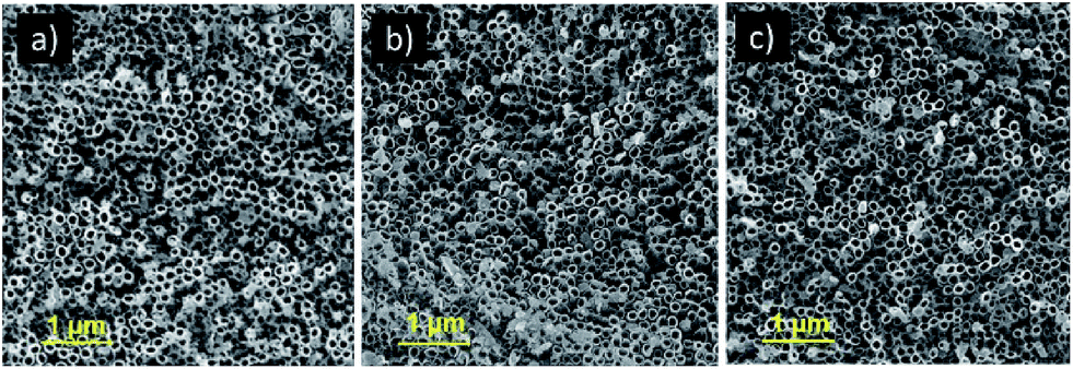 | ||
| Fig. 1 Surface SEM image of titania nanotube arrays: (a) pure, (b) I–TiO2–KI and (c) I–TiO2–HIO4. | ||
 | ||
| Fig. 2 High resolution SEM image of I–TiO2–HIO4 nanotube arrays. | ||
As it can be seen in Fig. 3, cross-section images for both types of iodine doped TiO2 together with EDX analysis at the top and at the bottom level of the titania layer were registered. The tube length for I–TiO2–KI and I–TiO2–HIO4 was 2.2 μm. Apart from the titanium and oxygen, iodine was detected on the same level at the base and at the surface section. This allows to form a conclusion that the electrochemical doping strategy leads to the introduction of iodine atoms across the entire layer thickness. The atomic concentration of iodine in I–TiO2–KI equals 0.31 at% and in I–TiO2–HIO4 sample equals 0.44 at%.
 | ||
| Fig. 3 Cross-section image of the titania nanotube layer of: (a) I–TiO2–KI and (b) I–TiO2–HIO4. | ||
In Fig. 4a and b the absorbance curves and the Tauc plot are given, respectively. As it is typical for titanium dioxide materials, the highest absorbance was registered in the UV range. An additional wide absorption band is present in the visible range with maximum at 550 nm which could be attributed to the presence of sub-bandgap states resulting from the unusual structure of titania nanotube12 or a considerable concentration of oxygen vacancies and other defects in the material.32 In the case of doped samples, the absorbance in the range of 450–700 nm is more intensive in comparison to the undoped sample. As it was reported by Wang et al.,33 different iodine forms can significantly affect the absorbance properties of TiO2.
 | ||
| Fig. 4 (a) Absorbance spectra and (b) the Tauc plot for pure and doped titania. | ||
Basing on the Tauc plot, the bandgap energy values were determined and equaled 2.95 and 3.0 eV for I–TiO2–KI, I–TiO2–HIO4, respectively, whereas for pure TiO2 Ebg = 3.07 eV. Therefore, both doped materials were characterized by narrower bandgap energy in comparison to pure titania. Such a change in Ebg value is typically observed for iodine doped titania nanoparticles34 and nanotubes as well.17 It should also be noted that the bandgap energy value determined for undoped titania differs from typical Ebg known for anatase nanoparticles (3.20 eV).35 It results from the presence of rutile, the oxide barrier layer at the interface Ti metal plate – titania nanotube layer. As it is known, the bandgap of rutile is lower than Ebg of anatase, thus the rutile phase at the interface shifts the absorption edge of the nanotube layer towards the visible range. Furthermore, differences between the absorbance ability of the nanotubular film and nanoparticles are strongly connected to the oxide gradient raised during the thermal annealing process and the tube length.9,36
The Raman spectra of pure TiO2 and iodine doped titania are shown in Fig. 5. Raman spectra show five bands typical for the anatase crystalline phase: at about 144, 196, 391, 514 and 634 cm−1 which are indexed to Eg(1), Eg(2), B1g, A1g and Eg(3) active modes, respectively. In general, the Raman spectra recorded for the undoped and iodine doped samples does not differ significantly, which indicates that the material has not changed structurally after the electrochemical treatment in iodine-containing electrolytes. However, a slight shift of Eg(1) maximum from 143.28 cm−1 registered for pure TiO2 to 144.12 cm−1 and 144.47 cm−1 for I–TiO2–HIO4, I–TiO2–KI, respectively, is observed. The shift could result from bonding of iodine to TiO2 or an increase of crystalline defects formed in the titanium dioxide framework due to the presence of iodine ions.37 According to Choudhury et al.,38 shifting of Eg(1) peak towards higher wavenumbers is caused by the introduction of dopant atoms which disturb Ti–O–Ti bonds and generate oxygen vacancies.
 | ||
| Fig. 5 Raman spectra of pure and iodine doped titania. | ||
The photoluminescence spectra of all nanotubular layers are shown in Fig. 6. The broad band with a maximum at 530 nm (2.34 eV) can be clearly observed for all samples and can be identified as surface states39 or as energy level at which deep trapped excitons can be located.40 In general, the value of luminescence is strongly connected to the radiative recombination of excited electrons and holes, i.e. the higher intensity of photoluminescence, the higher probability of electron–hole recombination. Among investigated materials, pure titania is characterized by the highest photoluminescence intensity which means that iodine doping participate in charge carrier separation36 and significantly inhibit radiative recombination processes.41 Thus, apart from the improved absorbance capability of I–TiO2 samples, the presence of iodine dopant atoms also leads to an increase of generated current during illumination.
 | ||
| Fig. 6 Photoluminescence spectra of pure and I-doped samples. | ||
The X-ray photoelectron spectroscopy allows to confirm iodine presence and to investigate the nature of elements in titania surface regions after the electrochemical doping procedure. Fig. 7 shows the high resolution XPS spectra for each element present in the doped samples. The XPS spectra as well as the position of each maxima recorded for pure titania nanotubes were described in our previous report.12 Table 1 summarizes the position of the deconvoluted peaks for doped nanotube arrays as well as for the undoped material. For all analyzed materials, the signals attributed to titanium, oxygen, carbon and iodine were detected. Additionally, for the I–TiO2–KI sample, a weak signal at 292.33 eV assigned to potassium was found. It could remain in titania nanotubes after their electrochemical treatment in a solution containing KI salt. The atomic ratio of Ti![[thin space (1/6-em)]](https://www.rsc.org/images/entities/char_2009.gif) :O:I is 1:2.57:0.080 and 1:2.48:0.063 for I–TiO2–KI and I–TiO2–HIO4 samples, respectively.
:O:I is 1:2.57:0.080 and 1:2.48:0.063 for I–TiO2–KI and I–TiO2–HIO4 samples, respectively.
 | ||
| Fig. 7 High resolution XPS spectra recorded at the oxygen, titanium, carbon and iodine region for (a) I–TiO2–HIO4 and (b) I–TiO2–KI samples. | ||
| Element | Core level | I–TiO2–KI [eV] | I–TiO2–HIO4 [eV] | TiO2 [eV] | |
|---|---|---|---|---|---|
| Iodine | I3d3/2 | 617.07 | 618.4 | 618.6 | — |
| I3d5/2 | 628.46 | 629.88 | 630.09 | — | |
| Titanium | Ti2p1/2 | 458.57 | 458.37 | 458.8 | |
| Ti2p3/2 | 464.3 | 464.09 | 464.4 | ||
| Oxygen | O1sA | 529.75 | 529.65 | 529.2 | |
| O1sB | 531.86 | 531.89 | 531.7 | ||
| Carbon | C1sA | 284.59 | 284.56 | 284.7 | |
| C1sB | 286.19 | 285.95 | 286; 288.7 | ||
The region attributed to titanium was characterized as doublet: Ti2p1/2 and Ti2p3/2. The positions of Ti2p1/2 are: 458.57 eV and 458.37 eV for I–TiO2–KI and I–TiO2–HIO4 respectively, that can be assigned to Ti4+ oxidation state.42 As it can be seen, the location of Ti2p peak found for both types of I–TiO2 materials is shifted towards the lower binding energy value in comparison to Ti2p observed for pure TiO2. The decrease of the Ti2p3/2 binding energy may be due to the formation of the new chemical arrangement I–Ti–O, as proposed by Wang et al.43 Iodine dopant is characterized by electronegativity below 0, thus a decrease in the electron density around Ti and the screening effect observed results in the increase of binding energy of Ti2p3/2.
The XPS region attributed to O1s was fitted using two singlets: O1sA and O1sB (see Fig. 7b). They correspond respectively to lattice oxygen and surface bound hydroxyl group44 or chemisorbed oxygen.42 The signals attributed to oxygen in iodine doped titania are located at higher energy value compared to the adequate position of O1s for pure titania. Such a notable shift of O1s maxima could be due to a partial substitution of oxidic states.45 A similar kind of conclusion had been derived for anionic doping of TiO2 nanoparticles by nitrogen and carbon.46
Apart from titania and oxygen, the signal attributed to carbon was detected in all investigated samples. The carbon C1s region is formed by two singlets.47 The highest carbon signal located at 284.59 eV (I–TiO2–KI) or 284.56 eV (I–TiO2–HIO4) could be assigned to C–C bonds and is regarded as a contaminant adsorbed on titania surface.48 Such carbon residues are typical for TiO2 nanotubes that were formed in electrolytes containing organic solvents, e.g. ethylene glycol49 or could be ascribed to possible carbon contamination from the instrument.50 The next peak found at 286.19 eV or 285.95 eV for I–TiO2–KI and I–TiO2–HIO4 respectively corresponds to oxygen bond carbon.51
The XPS spectra of I3d region show a clear doublet with peaks located at ca. 618 and 630 eV for both doped samples similarly to other I–TiO2 materials.52,53 There were no detectable peaks attributed to I7+ or I5+ at the binding energy of about 624 eV reported by Su et al.16 for I–TiO2 doped nanotubes synthesized using periodic acid as iodine precursor. According to Shi et al.,53 registered signals should be ascribed to negatively charged iodine species. Because iodine on 5+ or 7+ oxidation state exist in the form of iodiate (IO3−) or periodate (IO4−) and ionic radius of I− (0.216 nm) is much larger than that of O2− (0.124 nm) or Ti4+ (0.068 nm), the substitution of Ti4+ or O2− ions in the lattice by I− would hardly be probable. Therefore, it is possible that I− species are dispersed on the tube surface or at the interstitial sites of the TiO2 lattice. Nevertheless, the substitution of oxygen or titanium by any iodine species will significantly affect the anatase matrix.54
As it can be seen, the I-bands recorded for I–TiO2–KI were deconvoluted into two doublets, ascribed as: A (617.07 eV; 628.46 eV) and B (618.4 eV; 629.88 eV), whereas for I–TiO2–HIO4 single doublet (618.6 eV; 630.09 eV) was fitted. Until now, such deconvolution into two doublets was reported for iodine doped graphene oxide55 or bismuth oxide.56 According to Slimek et al.,57 they could be attributed to the multitude of chemical bonds, including elemental iodine, polyiodide anion: I3− and I5− with respective binding energies at 618.9 eV and 619.7 eV. However, on the contrary to I-doped graphene oxide or graphene,58 no Raman bands typical for I3− (109 cm−2) or I5− (167 cm−1) were registered. Additionally, Cabibil et al.59 also consider signals near 620 eV as C–I bonding. On the other hand, the analysis of iodine spectra registered for non-stoichiometric BOI1.5 was fitted with two sets of peaks similarly as in our case. One attributed to bulk iodine and another to I− from the excess of KI. Thus, because the presence of potassium traces was confirmed on the XPS survey spectra, the most likely interpretation of two doublets in the case of I–TiO2–KI can be attributed to the interstitial iodine and iodine present in KI residues. Nevertheless, we could conclude that high resolution XPS alone is not sufficient to precisely determine the type of iodine bonding within titania nanotubular structure and further specification using e.g. EXAFS should be undertaken.
The mechanism of iodine doping induced by the presence of periodic acid that was used as dopant precursor was proposed by Li et al.52 As it was reported, iodic acids form highly oxidative environment due to the presence of iodine with a high oxidation state characterized by high reactivity and ability to easily form multivalence iodine oxides: I2O5, I4O9. Such multivalence iodine species could accept oxygen atoms within the titania crystal lattice leading to the formation of the I–O–Ti arrangement that is with oxygen vacation. Here, oxygen vacancies are generated in the titania lattice, that is caused by the reduction process of periodic acid when iodine oxidation state of iodine (7+) is lowered to multi-valence states. During the electrochemical reduction process taking place at an electrode covered with nanotube arrays and immersed in periodic acid solution, the electrons released are involved in the generation of oxygen vacancies and simultaneously the electrons induce reduction of Ti4+ to Ti3+.
Reduction of periodic acid may proceed according to Lee et al.:60
| H5IO6 + H+ + e− → HIO3− + 3H2O | (3) |
Then, I5+ could be reduced to lower valence states:52 I5+ + 2e− → I3+ and/or 10I5+ + 10e− → 5I2↑.
These multi-valence states act as electron scattering sites that may influence efficient separation of charge carriers.61 As it was mentioned, the generation of oxygen vacancies: O → 1/2O2 + Vo2+ + 2e− takes place in parallel with the formation of the I–O–Ti bonds. In the case of the electrochemical process carried out in KI solution when 1.5 V is applied between the titania nanotubular anode and Pt mesh cathode, oxidation of iodide ions might proceed according to: 2I− − 2e− → I2; 3I− − 2e− → I3−, 2I3− − 2e− → 3I2. Thus, triiodide and iodide ions and iodine molecules can also be involved in possible doping phenomena.
Electrochemical characterization
Cyclic voltammetry was performed to characterize materials in contact with the deareated electrolyte (pH = 7). In Fig. 8, CV curves registered both for pure and iodine doped materials. The working electrode was polarized from the rest potential in the anodic direction up to 1 V and back up to −1 V vs. Ag/AgCl/0.1 M KCl. In general, the shape of CV curve is typical for titanium dioxide materials with a marginal capacitive current in anodic region (marked as A).62,63 However, in the case of doped materials, the clear reduction peak marked as B at −0.2 V vs. Ag/AgCl/0.1 M KCl is present that could be due to the presence of dopant atoms. According to Pelouchova et al.,64 this cathodic peak can be ascribed to the reduction of Ti4+ sites in TiO2. As a result of the electrochemical reaction, the change in the electronic structure of TiO2 takes place. This change is the formation of additional energy levels within the bandgap that significantly influences electrical conductivity as well as the optical properties of the material.3 At more negative potential when compared to the location of area B, the hydrogen evolution process is initiated. | ||
| Fig. 8 Cyclic voltammetry curves recorded for doped and pristine TiO2 immersed in 0.1 M K2SO4, v = 50 mV s−1. | ||
Electrochemical impedance spectroscopy was used to determine the space charge layer capacitance. The impedance spectra were recorded in the wide potential range, starting at the most anodic potential. The example impedance spectra is shown in Fig. 9a together with data points obtained from the fitting procedure. In order to analyze the collected spectra, the equivalent electric circuit (EEQC) was used: Re(CPE1R1)(CPE2R2W0) (see Fig. 9b) similar to that proposed by Munoz et al.65 The Re element corresponds to the electrolyte resistance. The following arrangement of electrical elements: (CPE1R1) and (CPE2R2W0) connected in series is attributed to a compact oxide thin film and ordered nanotubular layer, respectively.65 According to the approach proposed by Brug et al.,66 the CPE element is not pure capacitance, due to inhomogeneity of the electrode, but a constant phase element characterized by impedance Z = Q−1(iω)−α, where certain frequency dispersion α is taken into account. For the proposed fitting procedure, the value of α was in the range of 0.88–0.95. The CPE2 element strongly depends on the potential applied, whereas no significant dependency on the potential was observed for CPE2 value. The constancy of CPE1 element could be a consequence of the small reactivity of the oxide barrier layer.65
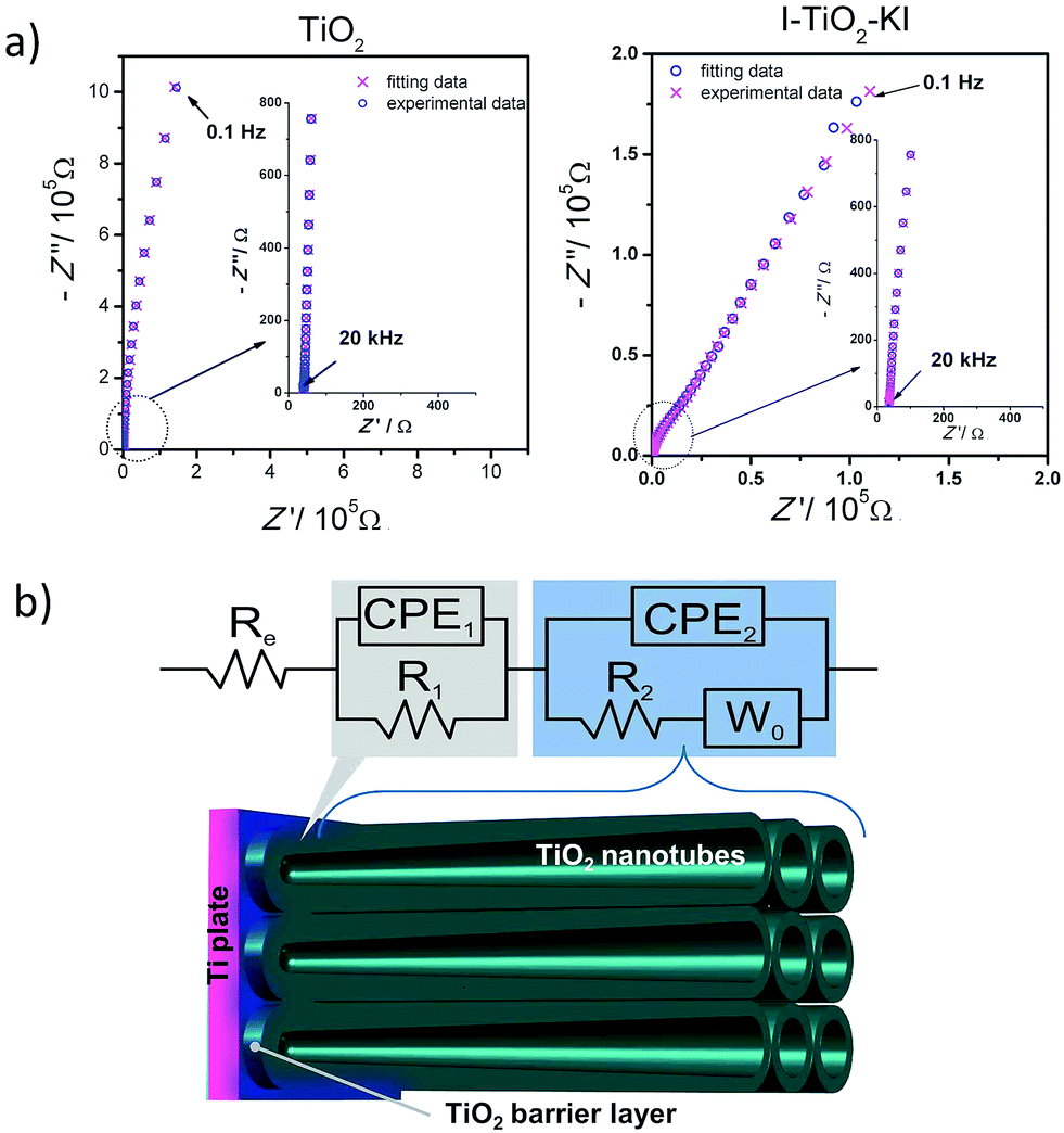 | ||
| Fig. 9 (a) An example of impedance spectra with experimental and fitting data obtained for TiO2 and I–TiO2–KI samples; (b) The scheme of electric equivalent circuit used for impedance spectra fitting for all tested materials. | ||
The Warburg open element (Wo), present in EEQC part attributed to the tubular layer, describes impedance of finite-length diffusion with reflective boundary as presented by this formula:
 | (4) |
Moreover, an attempt has been made to use a second diffusion impedance reflecting charge transport within the space inside the pores filled with electrolyte, however this approach does not improve fitting results. It is believed that even at the lowest frequencies measured, the electrode material, especially TiO2 barrier layer, does not allow the full penetration of electroactive species in the layer.67
Impedance data was used for further analysis using the Mott–Schottky relation which is expressed as:
 | (5) |
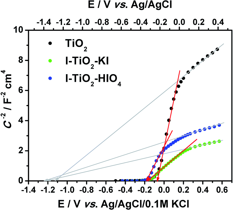 | ||
| Fig. 10 The Mott–Schottky plot for pure and iodine doped titanium nanotube array layers, C calculated from CPE2 taking into account α value. | ||
According to the Munoz approach, the flatband potential determined on the intercept of the Mott–Schottky function (in the range from +0.15 to −0.2 V vs. Ag/AgCl/0.1 M KCl) for pure titania is equal to −0.07 V vs. Ag/AgCl/0.1 M KCl whereas Efb for doped materials equals −0.16 V and −0.17 V vs. Ag/AgCl/0.1 M KCl for I–TiO2–HIO4 and I–TiO2–KI respectively. Taking into account the relation of C−2 vs. E in the positive range (from 0.15 V to 0.6 V vs. Ag/AgCl/0.1 M KCl), the flatband potential will be much more negative but still the Efb value for I–TiO2 will be catholically shifted in comparison to Efb determined for pure titania. According to Lee et al., presence of dopand can raise the conduction band edge.71 As it was mentioned above, the non-linear behavior of the Mott–Schottky plot could result from multiple donor levels that are ionized one after another.72 However, we should also take into account the fact that proper flatband determination can be made based on spectra collected at potentials more positive than and close to the flatband potential to avoid modification of conductive properties. As it was shown on the cyclic voltammetry curves, in the case of iodine doped materials, the reduction process takes place near −0.2 V vs. Ag/AgCl/0.1 M KCl and, in consequence, another element in EEQC attributed to the faradaic reaction should be introduced. Thus, data points on the Mott–Schottky plot present in the vicinity of reduction reaction should be interpreted carefully. Nevertheless, the determined flatband potential basing on C2− vs. E relation in the range of 0.15 to −0.2 V vs. Ag/AgCl/0.1 M KCl is reasonable and fits the range of potentials in which Efb for other nanotubular TiO2 layer was found.73–75
In situ spectroelectrochemical studies
The application of spectroelectrochemical measurements involving UV-vis spectroscopy together with simultaneous electrochemical measurements allows determination of the potential at which the initiation of electron injection to the available energy electron state occurs. The usage of a diffuse reflectance accessory instead of a transmission cell, broadens the UV-vis in situ spectroelectrochemistry application to non-transparent materials and is not influenced by the light scattering properties.In general, for titania materials, absorbance enhancement observed in the visible range is attributed to the increase in electron density in the conduction band.76 A more detailed analysis of absorbance spectra recorded for TiO2 nanotube arrays can be found in the previous section. As mentioned above, the absorbance maximum in the visible range for pure as well as for iodine doped samples was observed at 550 nm. Therefore, in analogy to the procedure proposed by Fritzmaurice,27,76 for semitransparent electrode, the change of the reflectance value upon applied potential was monitored at wavelength at which the maximum in absorbance was registered. In Fig. 11, the changes in reflectance at λ = 550 nm for pure TiO2 and iodine doped TiO2 at simultaneous changes in working electrode potential are shown.
 | ||
| Fig. 11 Relative reflectance measured as 550 nm as a function of applied potential for (a) pure TiO2, (b) I–TiO2–KI and (c) I–TiO2–HIO4, inset: reflectance converted to the Kubelka–Munk function. | ||
Additionally as the inset, transformation of reflectance into Kubelka–Munk function is given. The potential, at which the electron trapping process is initiated – Eon1, can be determined directly as the onset of reflectance changes or after recalculation – from Kubelka–Munk plot. In the case of pure titania, the onset of reflectance change was registered at −0.22 V vs. Ag/AgCl (−0.062 V vs. Ag/AgCl/0.1 MKCl), whereas Eon1 for I–TiO2–KI and I–TiO2–HIO4 equals −0.30 and −0.32 V vs. Ag/AgCl respectively (−0.142 V and −0.162 V vs. Ag/AgCl/0.1 M KCl). The value of Eon1 is assigned either to the flatband potential or the Fermi level.28 In other words, it describes the ability of materials to accept electrons. Because the onset potential observed for iodine doped titania is catholically shifted, they are characterized by improved capability towards electron acceptance. It should be noted that apart from the E1 onset potential, an additional rapid change in the run of reflectance changes vs. applied potential is observed. Such shape is associated with filling in trap states in the semiconductor electrode located either in the bulk, at grain boundaries or at the semiconductor/electrolyte interface.26 Trapping at grain boundaries is a possibility, however, trapping of electrons in surface states will most likely give rise to color changes at negative potentials.77 Thus, subsequent charge injection upon polarization yields the number of accumulated electrons as a function of the electrode potential applied during cathodic polarization.
The Eon1 value determined by in situ spectroelectrochemical measurements is very similar to the flatband potential value determined on the basis on the Mott–Schottky plot. Such consistency can be regarded as a strong Fermi level pinning, connected to the high concentration of surface states that causes matching between Ef and Eon1 values.78
Therefore, apart from the electrochemical impedance spectroscopy measurement, in situ spectroelectrochemical approach can be regarded as a useful method for Efb estimation. Further cathodic polarization leads to a subsequent decrease in relative reflectance and a clear change of the slope appears at the potential Eon2 – the same place at which the surface species undergo a faradaic reaction, see Fig. 8.
Photoactivity
Linear voltammetry (LV) was used to show magnitude of photocurrent generated under different applied potential to the titania electrode exposed to the UV-vis radiation of 100 mW cm−2. The photoelectrochemical behavior dependent on the applied potential of pure and iodine doped TiO2 is presented in Fig. 12. In the case of doped materials, a significant increase in photocurrent compared to pure titania nanotubes is recorded.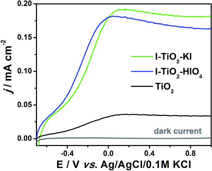 | ||
| Fig. 12 Linear voltammetry curves registered for iodine doped and pure titanium dioxide nanotube arrays under UV-vis illumination. | ||
The positive influence of a dopant is very likely due to the decrease of recombination processes and improved absorbance in the visible light as observed for other types of non-metal doped nanotube arrays.79,80
The chronoamperometry measurements facilitate the determination of the photocurrent retention at a constant potential and photoelectrode stability. Fig. 13 presents the transient photocurrent response of pure and iodine doped TiO2 nanotube arrays by on-off cycles registered under UV-vis and vis irradiation periods. The curve shows that the current rapidly increased and decreased when the radiation was switched on and off, respectively. The lack of steady current diminution suggests that the materials exhibit photocorrosion-resistance. Table 2 presents the values of photocurrent density registered after 10 min. of measurements and the ratios of respective photocurrents between the pure and doped TiO2 nanotubes. The highest saturated photocurrent was observed for I–TiO2–KI reaching 155.2 μA cm−2 and 3.1 μA cm−2 under UV-vis and vis illumination, respectively. Thus, the photocurrents were 6.06 and 5.07 times higher than the current registered for undoped TiO2 under the same light conditions. Despite the fact that photocurrent for I–TiO2–HIO4 is lower in comparison to I–TiO2–KI, the enhancement on a level of about 5 is still an impressive achievement that has not be reached for other non-metal doped titania nanotubes.24,77,81
 | ||
| Fig. 13 Amperometric current density–time curves at an applied potential of 0.5 V vs. Ag/AgCl/0.1 M KCl registered under (a) vis and (b) UV-vis irradiation. | ||
| Sample | Iph UV-vis/10−6 A cm−2 | Iph vis/10−7 A cm−2 |
|---|---|---|
| I–TiO2–KI | 155.2 (×6.06) | 30.9 (×5.07) |
| I–TiO2–HIO4 | 142.4 (×5.56) | 28.7 (×4.7) |
| TiO2 | 25.6 | 6.1 |
Photocatalytic properties
The photocatalytic activity of pure and iodine doped TiO2 nanotubes was investigated on the basis of the degradation progress of methylene blue (MB) as a model organic pollutant under UV-vis illumination. Fig. 14 presents the photocatalytic degradation of MB with an immersed titanium plate covered by TiO2, I–TiO2–KI and I–TiO2–HIO4. For comparison, a blank experiment under UV-vis irradiation without any sample was also performed. The slight decoloration of methylene blue solution is caused by a direct photolysis process induced by highly reactive radical species formed in the presence of irradiation.82 After a 2 h illumination in the presence of undoped titania nanotubes, the degradation of methylene blue reached 31%, whereas the degradation efficiency of 71% and 65% was observed for I–TiO2–KI and I–TiO2–HIO4, respectively. It is evident that the degradation of MB has been improved due to the doping of titania nanotubes with iodine which extends the absorption edges to the visible light region. In addition, the enhanced photocatalytic activity of doped titania nanotubes can be attributed to the more effective separation of the photogenerated electrons and holes. It is noteworthy that the application of the photocatalyst in the form of a solid plate immersed in contaminated fluid is advantageous in comparison to the common use of a catalyst suspension. | ||
| Fig. 14 Photocatalytic performance of the obtained samples under UV-vis illumination. | ||
D Conclusions
A simple method was proposed and optimized for the fabrication of photoactive and stable titania nanotube arrays doped with iodine. It was found that the electrochemical treatment in electrolyte containing iodine precursor (KI or HIO4), as an additional step after formation of titania nanotube arrays via anodization, does not affect their tubular architecture. All types of obtained materials formed uniform layers composed of ordered nanotube arrays with 2.2 μm length and 95 nm of internal diameter. The presence of iodine species was confirmed and investigated by the X-ray photoelectron spectroscopy technique. Iodine-doped samples were characterized by lower bandgap energy and decrease of photoluminescence in comparison with pure titania. The measurements carried out under sample irradiation showed that iodine doping radically improved photocatalytic activity as well as the generation of photocurrent. After 2 h of the photodegradation process for I–TiO2–KI and I–TiO2–HIO4 materials, the amount of methylene blue remaining in the solution respectively equaled 29% and 35% of its initial concentration, whereas when TiO2 was used as photocatalyst, it was equal to 69%. The enhancement of the current registered under UV-vis irradiation (100 mW cm−2) for iodine doped titania: I–TiO2–KI and I–TiO2–HIO4 is 6.06 and 5.56 times higher than pure TiO2. Furthermore, an investigation using the electrochemical impedance spectroscopy and in situ UV-vis spectroelectrochemical studies showed that electrochemical doping procedure induces noticeable changes of the electrochemical activity. This manifests as a different slope of the Mott–Schottky plot for doped and pure titania as well as a shift of the onset potential at which a decrease in reflectance is registered.In summary, because of the highly improved photoactivity of the doped materials when compared to pristine TiO2, iodine doped titania nanotubes show good potential for application as photoelectrodes in dye sensitized solar cells or for sustainable photocatalytic degradation of environmental hazardous substances. However, further studies concerning detailed investigations of the nature of iodine need to be carried out.
Acknowledgements
This work was financially supported by the Polish National Science Center: Grant no. 2012/07/D/ST5/02269. Authors are very thankful to Mrs K. Grochowska for visualization of nanotubular architecture.References
- P. Roy, S. Berger and P. Schmuki, Angew. Chem., Int. Ed., 2011, 50, 2904 CrossRef CAS PubMed
.
- G. K. Mor, O. K. Varghese, M. Paulose, K. Shankar and C. A. Grimes, Sol. Energy Mater. Sol. Cells, 2006, 90, 2011 CrossRef CAS PubMed
- J. M. Macak, H. Tsuchiya, A. Ghicov, K. Yasuda, R. Hahn, S. Bauer and P. Schmuki, Curr. Opin. Solid State Mater. Sci., 2007, 11, 3 CrossRef CAS PubMed
- D. Kowalski, D. Kim and P. Schmuki, Nano Today, 2013, 8, 235 CrossRef CAS PubMed
- G. D. Sulka, J. Kapusta-Kolodziej, A. Brzozka and M. Jaskuła, Electrochim. Acta, 2013, 104, 526 CrossRef CAS PubMed
- H. He, C. Liu, K. D. Dubois, T. Jin, M. E. Louis and G. Li, Ind. Eng. Chem. Res., 2012, 51, 11841 CrossRef CAS
- J. Lee, D. H. Kim, S. H. Hong and J. Y. Jho, Sens. Actuators, B, 2011, 160, 1494 CrossRef CAS PubMed
- H. F. Zhuang, C. J. Lin, Y. K. Lai, L. Sun and J. Li, Environ. Sci. Technol., 2007, 41, 4735 CrossRef CAS
- C. A. Grimes and G. K. Mor, Use of TiO2 nanotube arrays for biological applications, TiO2 nanotube arrays, Springer, 2009, pp. 285–314 Search PubMed
- A. Matsuda, S. Sreekantan and W. Krengvirat, J. Asian Ceram. Soc., 2013, 1, 203 CrossRef PubMed
- S. Kurian, H. Seo and H. Jeon, J. Phys. Chem. C, 2013, 117, 16751 Search PubMed
- K. Siuzdak, M. Szkoda, M. Sawczak and A. Lisowska-Oleksiak, New J. Chem., 2015, 39, 2741 RSC
- X. Tang and D. Li, J. Phys. Chem. C, 2008, 112, 5405 CAS
- Y. Zhang, W. Fu, H. Yang, S. Liu, P. Sun, M. Yuan, D. Ma, W. Zhao, Y. Sui, M. Li and Y. Li, Thin Solid Films, 2009, 518, 99 CrossRef CAS PubMed
- G. G. Bessegato, J. C. Cardoso and M. V. B. Zanoni, Catal. Today, 2015, 240, 100 CrossRef CAS PubMed
- Y. Su, Y. Xiao, X. Fu, Y. Deng and F. Zhang, Mater. Res. Bull., 2009, 44, 2169 CrossRef CAS PubMed
- Y. Su, Y. Xiao, Y. Du and S. Fu, Chin. Sci. Bull., 2010, 55, 2136 CrossRef CAS
- A. W. Bott, Curr. Sep., 1998, 17, 87 CAS
- J. O. 'M. Bockris and S. U. M. Khan, Surface Electrochemistry, a Molecular Level Approach, Plenum Press, New York, 1993, pp. 170–173 Search PubMed
- A. M. Roy, G. C. d. N. Sasmal and S. S. Bhattacharyya, Int. J. Hydrogen Energy, 1995, 20, 627 CrossRef CAS
- M. D. Ward, J. R. White and A. J. Bard, J. Am. Chem. Soc., 1983, 105, 27 CrossRef CAS
- R. Beranek and H. Kisch, Electrochem. Commun., 2007, 9, 761 CrossRef CAS PubMed
- M. Hepel and S. Hazelton, Electrochim. Acta, 2005, 50, 5278 CrossRef CAS PubMed
- X. Cheng, H. Liu, Q. Chen, J. Li and P. Wang, Electrochim. Acta, 2013, 103, 134 CrossRef CAS PubMed
- G. Boschloo and D. Fitzmaurice, J. Phys. Chem. B, 1999, 103, 7860 CrossRef CAS
- G. Boschloo and D. Fritzmaurice, J. Phys. Chem. B, 1999, 103, 2228 CrossRef CAS
- G. Redmond and D. Fitzmaurice, J. Phys. Chem., 1993, 97, 1426 CrossRef CAS
- E. Świętek, K. Pilarczyk, J. Derdzińska, K. Szaciłowski and W. Macyk, Phys. Chem. Chem. Phys., 2013, 15, 14256 RSC
- A. S. R. Bondarenko and G. A. Ragoisha, Inverse Problem in Potentiodynamic Electrochemical Impedance, in Progress in Chemometrics Research, ed. A. L. Pomerantsev, Nova Science Publishers, New York, 2005, pp. 89–102 Search PubMed
- L. Lu, B. H. Brown, D. C. Barber and A. D. Leathard, Physiol. Meas., 1995, 16, A39 CrossRef CAS
- K. Yasuda and P. Schmuki, Electrochim. Acta, 2007, 52, 4053 CrossRef CAS PubMed
- Y. Li, Y. Jiang, S. Peng and F. Jiang, J. Hazard. Mater., 2010, 182, 90 CrossRef CAS PubMed
- W. Wang-an, S. Qian, W. Yu-ping, C. Jin-li, L. Guo-qing and P. Pan-yang, Appl. Surf. Sci., 2011, 257, 3688 CrossRef PubMed
- A. Lisowska-Oleksiak, K. Szybowska and V. Jasulaitiene, Electrochim. Acta, 2010, 55, 5881 CrossRef CAS PubMed
- W. J. Yin, S. Chen, J. H. Yang, X. G. Gong, Y. Yan and S. H. Wei, Appl. Phys. Lett., 2010, 96, 221901 CrossRef PubMed
- K. G. Ong, O. K. Vargheseand, G. K. Mor and C. A. Grimes, J. Nanosci. Nanotechnol., 2005, 5, 1 CrossRef PubMed
- S. Bagwasi, B. Tian, F. Chen, F. Chen and J. Zhang, Appl. Surf. Sci., 2012, 258, 3927 CrossRef CAS PubMed
- B. Choudhury, M. Dey and A. Choudhury, Int. Nano Lett., 2013, 3, 25 CrossRef
- L. Forss and M. Schubnell, Appl. Phys. B, 1993, 56, 363 CrossRef
- J. H. Jang, K. S. Jeon, T. S. Park, K. W. Lee and M. Yoon, J. Chin. Chem. Soc., 2006, 53, 123 CrossRef CAS PubMed
- E. Wang, T. He, L. Zhao, Y. Chen and Y. Cao, J. Mater. Chem., 2011, 21, 144 RSC
- Q. Zhang, Y. Li, E. A. Ackerman, M. Gajdardziska-Josifovska and H. Li, Appl. Catal., A, 2011, 400, 195 CrossRef CAS PubMed
- Y. Wang, J. Ren, G. Liu and P. Peng, Mater. Chem. Phys., 2011, 130, 493 CrossRef CAS PubMed
- Y. Ma, J. W. Fu, X. Tao, X. Li and J. F. Chen, Appl. Surf. Sci., 2011, 257, 5046 CrossRef CAS PubMed
- S. Anandan, K. Kathiravan, V. Murugesan and Y. Ikuma, Catal. Commun., 2009, 10, 1014 CrossRef CAS PubMed
- J. Yang, H. Bai, X. Tan and J. Lian, Appl. Surf. Sci., 2006, 253, 1988 CrossRef CAS PubMed
- A. L. Cui, T. J. Wang and Y. Jin, Eng. Chem. Metall., 1999, 20, 178 CAS
- T. T. Isimjan, A. El Ruby, S. Rohani and A. K. Ray, Nanotechnology, 2010, 21, 55706 CrossRef PubMed
- J. Zhang, B. Gao, Q. Gan, J. Xia, Y. Cao, J. Wang and K. Huo, Chem. Rapid Commun., 2014, 2, 29 Search PubMed
- Y. Li, G. Ma, S. Peng, G. Lu and S. Li, Appl. Surf. Sci., 2008, 254, 6831 CrossRef CAS PubMed
- J. H. Yun, R. J. Wong, Y. H. Ng, A. Du and R. Amal, RSC Adv., 2012, 2, 8164 RSC
- W. Li, R. Liang, A. Hu, Z. Huang and Y. Norman Zhou, RSC Adv., 2014, 4, 36959 RSC
- N. Shi, X. Li, T. Fan, H. Zhou, J. Ding, D. Zhang and H. Zhou, Energy Environ. Sci., 2011, 4, 172 CAS
- K. Yang, Y. Dai, B. Huang and M. H. Whangbo, Chem. Mater., 2008, 20, 6528 CrossRef CAS
- J. Wang, B. Li, T. Ni, T. Dai and Y. Lu, Compos. Sci. Technol., 2015, 109, 12 CrossRef CAS PubMed
- X. Zhang and L. Zhang, J. Phys. Chem. C, 2010, 114, 18198 CAS
- P. Slimek, K. Klimowa, D. Sedmidubsky, O. Jankovsky, M. Pumera and Z. Sofer, Nanoscale, 2015, 7, 261 RSC
- G. Kalita, K. Wakita, M. Takahashi and M. Umeno, J. Mater. Chem., 2011, 21, 15209 RSC
- H. Cabibil, H. ihm and J. M. White, Surf. Sci., 2000, 447, 91 CrossRef CAS
- B. Lee, D. J. Duquette and R. J. Gutmann, Chemical–mechanical polishing of copper with model slurries, Electrochemical science and Technology of Copper, 2002 Search PubMed
- W. Y. Su, Y. F. Zhang, Z. H. Li, L. Wu, X. X. Wang, J. Q. Li and X. Z. Fu, Langmuir, 2008, 24, 3422 CrossRef CAS PubMed
- H. Du, Y. Xie, C. Xia, W. Wang and F. Tian, New J. Chem., 2014, 38, 1284 RSC
- H. Yu, J. Ma, Y. Zhang, X. Zhang and W. Shi, Electrochim. Acta, 2011, 56, 6498 CrossRef CAS PubMed
- H. Pelouchova, P. Janda, J. Wber and L. Kavan, J. Electroanal. Chem., 2004, 566, 73 CrossRef CAS PubMed
- A. G. Munoz, Q. Chen and P. Schmuki, J. Solid State Electrochem., 2007, 11, 1077 CrossRef CAS
- G. J. Brug, A. L. G. Van Den Eeden, M. Sluyters-Rehbach and J. H. Sluyters, J. Electroanal. Chem., 1984, 176, 275 CrossRef CAS
- A. J. Roberts and R. C. T. Slade, ECS Trans., 2010, 28, 33 CAS
- A. Hagfeldt, U. Bjorkstein and M. Gratzel, J. Phys. Chem., 1996, 100, 8045 CrossRef CAS
- D. B. Bonham and M. E. Orazem, J. Electrochem. Soc., 1992, 139, 127 CrossRef CAS PubMed
- Z. Wang, J. Zhao, X. Wang and J. Zhou, IEEE Trans. Nanotechnol., 2015, 14, 113 CrossRef
- Y. Li, Y. Xiang, S. Peng, X. Wang and L. Zhu, Electrochim. Acta, 2013, 87, 794 CrossRef CAS PubMed
- E. J. Lee and S. I. Pyun, J. Appl. Electrochem., 1992, 22, 156 CrossRef CAS
- I. Hanzu, T. Djenizian and P. Knauth, J. Phys. Chem. C, 2011, 115, 5989 CAS
- Y. Tan, S. Zhang and K. Liang, Nanoscale Res. Lett., 2014, 9, 67 CrossRef PubMed
- R. Beranek, H. Tsuchiiya, T. Sugishima, J. M. Macak, L. Taveira, S. Fujimoto, H. Kisch and P. Schmuki, Appl. Phys. Lett., 2005, 87, 243114 CrossRef PubMed
- G. Rotherberger, D. Fritzmaurice and M. Gratzel, J. Phys. Chem., 1992, 96, 5983 CrossRef
- F. Cao, G. Oskam, P. C. Searson, J. M. Stipkala, T. A. Heimer, F. Farzad and G. J. Meyer, J. Phys. Chem., 1995, 99, 11974 CrossRef CAS
- T. Berger, J. A. Anta and V. Morales-Florez, J. Phys. Chem. C, 2012, 116, 11444 CAS
- S. Li, L. Yang, S. Xu, S. Luo and Q. Cai, Electrochem. Commun., 2009, 11, 1748 CrossRef PubMed
- H. Li, J. Xing, Z. Xia and J. Chen, Electrochim. Acta, 2014, 139, 331 CrossRef CAS PubMed
- S. Liu, L. Yang, S. Xu, S. Luo and Q. Cai, Electrochem. Commun., 2009, 11, 1748 CrossRef CAS PubMed
- J. Li, N. Lu, X. Quan, S. Chen and H. Zhao, Ind. Eng. Chem. Res., 2008, 47, 3804 CrossRef CAS
Footnote |
| † Electronic supplementary information (ESI) available. See DOI: 10.1039/c5ra08407e |
| This journal is © The Royal Society of Chemistry 2015 |