
 Open Access Article
 This Open Access Article is licensed under a
 Creative Commons Attribution 3.0 Unported Licence
The effect of nanoparticle size on calendar and cycle lifetimes of silicon anode lithium-ion batteries†
Juliane I.
Preimesberger
 a,
Francois L. E.
Usseglio-Viretta
b,
Ankit
Verma
b,
Avtar
Singh
b,
Andrew M.
Colclasure
b,
Patrick
Walker
a,
Glenn
Teeter
a,
Gregory F.
Pach
a,
John
Westgard
a,
Fernando
Urias-Cordero
a,
Nathan R.
Neale
cd,
Jaclyn E.
Coyle
*a and
G. Michael
Carroll
*a
a,
Francois L. E.
Usseglio-Viretta
b,
Ankit
Verma
b,
Avtar
Singh
b,
Andrew M.
Colclasure
b,
Patrick
Walker
a,
Glenn
Teeter
a,
Gregory F.
Pach
a,
John
Westgard
a,
Fernando
Urias-Cordero
a,
Nathan R.
Neale
cd,
Jaclyn E.
Coyle
*a and
G. Michael
Carroll
*a
aMaterials Sciences Center, National Renewable Energy Laboratory, 15013 Denver West Parkway, Golden, Colorado 80401, USA. E-mail: Mike.Carroll@nrel.gov; Jaclyn.Coyle@nrel.gov
bEnergy Conversion and Storage Systems Center, National Renewable Energy Laboratory, Golden, Colorado 80401, USA
cChemistry and Nanoscience Center, National Renewable Energy Laboratory, 15013 Denver West Parkway, Golden, Colorado 80401, USA
dRenewable and Sustainable Energy Institute, University of Colorado Boulder, Boulder, Colorado 80309, USA
First published on 11th February 2025
Abstract
Next-generation rechargeable lithium-ion battery anodes must have high energy densities, low costs, and excellent cycle and calendar lifetimes to replace graphite as the incumbent chemistry. Silicon is well positioned to meet these requirements but face two obstacles before reaching commercialization: silicon's large volume expansion during charge cycling causes significant mechanical degradation, and the silicon surface is highly reactive, causing rapid irreversible capacity loss both during cycling and at rest. One strategy to address the mechanical degradation is to use silicon nanoparticles that are small enough to withstand the volume changes without mechanical pulverization. However, even small nanoparticles that won't fracture will still transmit strain across the electrode during battery cycling. Moreover, conventional wisdom says decreasing the particle size will accelerate parasitic chemistry to reduce the calendar life as the total surface area increases. In this work, we show that smaller silicon nanoparticles (∼6 nm) have higher cycle lifetimes than larger nanoparticles (∼27 nm) because there is less mechanical damage to the electrode. Moreover, we show that no significant difference in calendar lifetimes between nanoparticle sizes exists, due to the very dense electrode structure that is formed, which limits the surface area that is exposed to electrolyte. These results provide important information for accurately assessing the role of particle size in silicon-based LIB anodes.
Broader contextBattery-powered electric vehicles are a promising solution for integrating transportation into the electric grid. However, there is yet to be widespread consumer adoption of electric vehicles, in part due to higher costs, smaller vehicle mileage ranges, and inconvenience of slow charging. Important targets for new battery chemistries that could encourage electric vehicle use include low costs, large driving ranges, many cycles, and long shelf-lives. Current, commercial rechargeable lithium-ion batteries with graphite anodes have too low energy-density to reach the first two goals, but different anode chemistries such as silicon could achieve the cost and range targets. There are still barriers before silicon anodes can replace graphite anodes, however, due to the large volume expansion of silicon during lithiation and its highly reactive surface, both of which contribute to irreversible capacity loss. |
Introduction
The current, commercialized lithium-ion batteries use graphite as an anode material, as it can deliver several thousand charge–discharge cycles, is chemically stable for many years even when the battery is not in use (typically referred to as calendar life) and can be produced and processed into electrodes at commercially relevant scales. However, graphite's theoretical gravimetric energy density (372 mA h g−1) is too low to enable electric vehicles to compete with internal combustion engines: batteries must have a low cost (less than $100 per kW per h) and enable long range vehicles (at least 300 miles between charges).1 Other important targets for new battery chemistries include batteries that can cycle more than 1000 times, and age for more than 10 years before reaching 80% of its initial capacity (the threshold for a battery's useful life).2High-silicon content anodes are a promising candidate to reach these targets, as silicon has a much higher theoretical energy density (3500 mA h g−1) than graphite, is earth-abundant, and already has mature technologies from the semiconductor chip and photovoltaic sectors for its processing and purification.3–5 However, silicon (Si) anodes still face many challenges before the chemistry can compete with graphite. As silicon can store larger stoichiometric amounts of lithium than graphite, resulting in silicon's higher energy density, full lithiation of silicon results in very large volume expansions (over 300% compared to only 10% for graphite).3 This volume expansion during charge-cycling causes significant mechanical damage to the anode during battery cycling, which contributes to fast capacity fade. Additionally, silicon is difficult to passivate, due to the high reactivity of the silicon surface and continued volume changes during cycling which break apart any passivating layer that is formed.6–8
Particle rupturing as a function of silicon particle size has been demonstrated as a major contribution to capacity fade in silicon anode batteries.9 It is typically expected that silicon NPs below ∼150 nm are unlikely to rupture even with large volume expansions.9–11 However, particles below this limit will still expand, and even with the same total strain (300%) across particle sizes, expanded larger particles will displace more total volume of the composite electrode than smaller particles, which would cause more mechanical damage and loss of active material connectivity. Also, smaller particles tend to lithiate faster in lithium-ion battery materials, likely due to smaller diffusion lengths which result in faster solid-state diffusion and more homogeneous (de)lithiation.12–14 Therefore, we would expect smaller NPs to provide better cyclability; however, conventional wisdom in the battery community indicates that the increase in surface area of smaller NPs would result in more irreversible side reactions that contribute to capacity fade.15 This is particularly important in Si anodes due to the challenges in surface passivation.
To combat this problem of increased surface area, one potential solution is to structure the particles into larger agglomerates, to protect the surfaces of nano-crystallites from electrolyte contact. This micro-structuring technique can be found in commercial high-performing cathode systems such as nickel–manganese–cobalt oxide particles (NMC) which are comprised of nano-crystallites arranged in a micron-sized spherical particle.16–18 There is a preponderance of evidence that this strategy could be useful for silicon anodes. However, micro-structured Si electrodes tend to either have high porosities, which make meeting energy-density targets challenging, or require different electrode processing techniques, which pose barriers to industry-level scale up and production.19–28
Recent progress on high-silicon content anodes has demonstrated that careful control of surface chemistries and the use of very small (<10 nm) silicon nanoparticles allows for an anode that can deliver more than a thousand charge–discharge cycles.29–31 Hydrophilic coatings on silicon nanoparticles act as an electric insulator and ionic conductor, similar to an ideal solid electrolyte interphase (SEI), and this surface functionalization promotes good nanoparticle dispersion in solution, resulting in more-stable slurries and ideal composite electrodes.29,30 While these silicon NPs can reach the energy density and cycle life metrics needed, there is still a technical gap between current silicon anode calendar aging performances and the 10-year target, which means that the characterization of silicon anode performance is not complete without calendar aging.32 To the authors’ knowledge, there is yet to be a study investigating how important the size of ultra-small nanoparticles (well below the rupture limit of 150 nm) is to the cycle and calendar aging performance of Si anodes.
To address this knowledge gap, we investigate the role of silicon particle size on anode cycle stability and calendar life. Through systematic particle size synthesis and integration into composite anodes, we find that smaller NPs have better cycle life than larger NPs, and counter-intuitively, there is no significant difference in calendar life. We show that despite the larger surface-to-volume ratio of small NPs, the dense microstructure afforded by these small Si NPs limit the electrolyte contact with the Si, enabling the use of smaller NPs without increasing parasitic reactions. Notably, we find that while the volume expansion of Si NPs affects the structural integrity of the electrode, smaller NPs cause less damage, which we hypothesize contributes to their improved cycle stability.
Methods
Nanoparticle preparation
Silicon nanoparticles ranging from 3–27 nm in diameter were made using a plasma-enhanced chemical vapor deposition (PECVD) process, in a custom nonthermal RF-enhanced plasma reactor.29,33–35 Growth conditions are shown in the ESI, Table S1.† Average particle diameters were confirmed by X-ray diffraction, shown in Fig. S1.† Nanoparticles were surface-coated with an excess volume (∼10 mL) of allyloxy (poly)ethylene oxide (PEO), where the oligomer length was chosen such that the molecular coating was approximately 20% of the total particle weight assuming an average packing density of 2 PEO nm−2.29 An excess (5–10 mg) of a radical initiator azobis-cyclohexanecarbonitrile (ABCN) was added to the PEO and nanoparticle mixture, and the particles were left to react at 220 °C for at least 3–4 days, stirring constantly.29,30 Then the particles were washed with toluene (∼10 mL) and hexane (∼20 mL) and centrifuged at 12![[thin space (1/6-em)]](https://www.rsc.org/images/entities/char_2009.gif) 500g for five minutes. The supernatant was decanted, and the particles were centrifuged a second time with fresh toluene and hexane.29 The particles were dried under vacuum, weighed, and suspended in N-methyl pyrrolidone (NMP) at 100 °C and mixed overnight. Table S2† reports the weight percentages of Si@PEO in NMP for each particle size; if a mixture was too viscous (which was typical for smaller particle sizes) more NMP was required. Previous reports on these coated nanoparticles confirm that they form uniform colloidal suspension in NMP, which is essential for homogeneous slurry formulation, and is why it is necessary to coat these nanoparticles with PEO, as their native surface chemistry is too reactive to form homogenous slurries.29,30 It was more difficult to suspend the 3 and 4 nm Si@PEO NPs in solution than the other particles, indicating that the quality of the PEO coating was not as good for these particles, which might have affected slurry formulation and subsequent electrochemical performance.
500g for five minutes. The supernatant was decanted, and the particles were centrifuged a second time with fresh toluene and hexane.29 The particles were dried under vacuum, weighed, and suspended in N-methyl pyrrolidone (NMP) at 100 °C and mixed overnight. Table S2† reports the weight percentages of Si@PEO in NMP for each particle size; if a mixture was too viscous (which was typical for smaller particle sizes) more NMP was required. Previous reports on these coated nanoparticles confirm that they form uniform colloidal suspension in NMP, which is essential for homogeneous slurry formulation, and is why it is necessary to coat these nanoparticles with PEO, as their native surface chemistry is too reactive to form homogenous slurries.29,30 It was more difficult to suspend the 3 and 4 nm Si@PEO NPs in solution than the other particles, indicating that the quality of the PEO coating was not as good for these particles, which might have affected slurry formulation and subsequent electrochemical performance.
Slurry and electrode preparation
Slurries were made with 89 wt% Si (not including the weight of the PEO coating, as it is removed during annealing), 1 wt% single-walled carbon nanotubes (SWCNTs), and 10 wt% polyimide binder (P84). The CNTs (Tuball™ Batt NMP, 97% NMP, 2% polyvinylidene fluoride (PVDF), and 1 wt% SWCNT) were added to the Si@PEO and NMP solution and stirred for at least 4 h. The binder (polyimide P84, 5 wt% solution in NMP) was then added to the slurry. The slurry was planetary mixed (using a Mazerustar KK-250S planetary mixer, at a rotation rate of 430 rpm and revolution rate of 1450 rpm for 270 s, followed by 60 s of 1700 rpm rotation and 1700 rpm revolution rate) and left to stir overnight. Right before casting the electrode, the slurry was planetary mixed for an additional 180 s (at revolution and rotation rates of 1700 rpm). Slurries were blade coated onto roughened copper foil (18 μm nominal thickness) using a Zehntner ZAA 2300 automatic film applicator with a casting speed of around 1 cm s−1. Two thicknesses for each particle size were cast. To account for the different slurry viscosities found in smaller particles, wet gaps were normalized to 50 and 100 μm for a slurry with 10 wt% Si (where the total weight includes the NMP and other components). Therefore, a slurry with 12.5 wt% Si would have wet gaps of 40 and 80 μm.After casting, electrodes were dried in a vacuum oven at 150 °C for four hours, and then annealed under nitrogen in a tube furnace at 550 °C for four hours. Weight calculations for the 89/1/10 wt% ratio assumed that all the PEO and PVDF are burned off during this annealing step. Previous studies have demonstrated that it is essential to burn off the PEO surface coating prior to electrochemical cycling, as the PEO limits the capacity of the electrode and hinders cyclability.30 After annealing, the surface of the nanoparticles is silicon oxide, as surface characterization indicates the PEO does not leave behind a carbon layer.30 The polyimide binder is chosen because it is stable at this annealing temperature, and undergoes cross-linking, which improves the mechanical integrity of the electrode.30
Coin cell fabrication and testing
All coin cells were made in a 2032 configuration, with a 19 mm diameter Celgard 2325 separator and 40 μL of electrolyte (1.2 M lithium hexafluorophosphate LiPF6 in EC:EMC 3:7 w/w with 3 wt% fluoroethylene carbonate added). Coin cells were cycled with a Maccor 4300 tower in a temperature-controlled oven. Half cells were made with a 14 mm diameter Si electrode against a 9/16′′ diameter Li metal reference (Alfa Aesar 10769, 0.75 mm thick, 99.9% metals basis) to check the capacity of each electrode (voltage range 0.01–1.5 V, temperature 30 °C, C/20 rate). The electrodes with an areal capacity closest to 0.8 mA h cm−2 were chosen for this study. Half-cell results are reported in the ESI, Fig. S2–S5.†
Full cells were made with a 15 mm diameter Si anode and a 14 mm diameter LFP cathode (1.7 mA h cm−2 at C/10, 92 wt% Johnson Matthey LFP, with 3.9 wt% Timcal C-45, 0.1 wt% Tuball™ Batt NMP SWCNT, and 4 wt% Solvay 5130 PVDF) fabricated by the Cell Analysis, Modeling, and Prototyping (CAMP) facility at Argonne National Laboratory. LFP was chosen to avoid aging contributions from the cathode, such as the voltage slipping problem that occurs in NMC cathodes, as LFP's voltage profile is flat. Full cells were formed with a four-hour rest followed by two full C/10 cycles (2.7–3.4 V), a 48 hours hold at 3.4 V to allow the electrolyte to wet the anode, and then ten C/3 cycles. Cells were formed at the same temperature as the following protocols. Calendar aging was tested at 45 °C, with three C/10 cycles followed by a hybrid pulse power characterization (HPPC) step, every 30 days. During the 30-day aging period, a daily pulse discharge at 1C was applied to test the impedance rise of the cells, and then the cells were then charged back to 3.4 V. Additional cells at 45 °C performed only the three C/10 cycles and HPPC protocol, without the 30-day calendar aging in between, to account for the aging effects of cycling. Cycle aging at C/3 was tested at 30 °C, with three C/10 cycles and a HPPC steps repeated every 50 C/3 cycles. Electrochemical protocols are plotted in Fig. S6.†
Microstructure experimental characterization
Cross-sections of pristine and cycled electrodes were made using a JEOL cooling cross-section ion beam (IB-19520CCP). A Hitachi S-4800 scanning electron microscope (SEM) was used to image the cross-sections, at 3 kV energy and 7 μA current.To characterize electrode electrochemically active surface area (ECSA), symmetric 2032-type coin cells were made, with two 15 mm diameter pristine Si electrodes, a glass fiber separator, and 100 μL 0.5 M tetrabutylammonium hexafluorophosphate (TBAPF6) in EC:EMC 3:7 w/w as a blocking electrolyte that cannot alloy with Si. A BioLogic® VMP3 potentiostat was used to measure cyclic voltammetry (CV), from −0.1 to 0.1 V at five different sweep rates (10, 20, 30, 40 and 50 mV s−1).36,37 The specific capacitance of silicon was measured using the symmetric cell setup with a thin film (60 nm thick) of Si sputtered onto copper; it was assumed this thin film was approximately flat.
Microstructure computational modeling
Four-phases (i.e., pore, Si, SWCNT, and P84) anode microstructures were modeled using the Microstructure Analysis Toolbox (MATBOX), an open-source collection of algorithms for segmentation, characterization, numerical generation and meshing of heterogenous microstructures embedded in a user-friendly graphic user-interface38,39 and available at ref. 40. Microstructures are first numerically generated up to a defined porosity and weight loading, and then other metrics (e.g., interface area) are characterized. Details of the generation algorithms are available in an upcoming paper and briefly summarized here.41Silicon particles are generated using a stochastic algorithm with overlapping control to overcome packing density limit while maintaining spherical shape. SWCNTs are generated using another stochastic algorithm which samples candidate locations for implicit control points of 3D Bezier curves. Particles and tubes are allowed to be in contact but cannot overlap through the use of masks. While the generation tool allowed multi-modal size distributions, microstructures were generated with a single particle and tube diameter for a simpler interpretation of the results. Four Si diameters (3, 9, 15 and 30 nm) and one SWCNT diameter (2.75 nm) were investigated. SWCNT length (∼1–5 μm) vastly exceeds the generated field of view (a cubic domain with 135 nm length), therefore tube length was not limited in the generation. The order of generation between different phases is constrained by the difficulty to generate them. For instance, generating large objects in a dense domain already filled with smaller objects is more challenging than the opposite. Also, generating tubes in a dense domain is more challenging than for particles, as each tube requires finding a sequence of implicit control points for the 3D Bezier curve that does not result in an overlap with any pre-existing objects, while particles require finding only one location. Therefore, tubes were generated first, except for the 30 nm Si diameter case. For the latter, tube orientation is de-facto controlled by the location of the silicon particles. For the other particle diameters, the orientation of the tubes is either isotropic or transversal anisotropic (Fig. S19†).
Binder phase is systematically generated last using a distance-based deterministic algorithm that glues together solid components not far from each other while letting the largest pores be vacant.42 For microstructures with dense silicon particles agglomerates, this results in removing Si-pore interfaces within the agglomerates (as distances are much smaller within the agglomerates), while letting the outer surface of the agglomerates be mostly binder-free. While real distribution of the binder is unknown at this scale, this approach is nevertheless coherent with the calendar life not being penalized with using small Si particles, as only the agglomerate surface is susceptible to parasitic reactions with the as-generated microstructures.
All microstructures have been generated with 1 wt% SWCNT, 10 wt% P84, and 89 wt% Si. Three porosities (20, 30, 40%) have been investigated. While the theoretical maximum density for unisize sphere packing is 74%, a more relevant limit, not based on an ideal periodic packing, for electrode microstructures is the maximum density for randomly distributed unisize spheres, estimated at 63.4%.43,44 The minimum porosity achievable without overlapping is thus only 36.6%. This means it is unavoidable to have some overlapping between the particles.
Interface area between pore and silicon particles and between multiple silicon particles are then calculated by summing the area of voxels in contact between the two phases (or between two particles in contact). Surface overestimation due to voxel discretization is amended applying a 2/3 corrective factor.45 Specific interface area is then deduced by normalizing it with the domain's volume.
Results and discussion
Cycle and calendar lifetimes
Full coin cells were made with an approximately 0.8 mA h cm−2 silicon anode paired with an oversized 1.7 mA h cm−2 lithium iron phosphate (LFP) cathode. LFP was chosen for its flat voltage plateau, to minimize any impact the cathode had on cycle and calendar aging. Silicon utilizations varied across electrodes, so the N/P ratio (anode capacity to cathode capacity) of the full cells ranged from 0.40 to 0.85 after formation; see Fig. S7 and Table S3† for further discussion. Periodic reference performance testing (RPT) steps were performed to check cell capacity and impedance, with a single RPT test composed of three C/10 cycles and a hybrid pulse power characterization (HPPC) step. Cycle lifetimes were tested at a C/3 rate, with an RPT step every 50 cycles.The average relative discharge capacity of the C/3 cycling cells is plotted in Fig. 1a. Shaded regions indicate standard deviations from 2–3 replicate cells (see Fig. S8† for a larger format of Fig. 1a, for clarity). In general, as particle size decreases, the capacity retention increases, resulting in better cycle performance. We note that the 3 and 4 nm electrodes do not perform better than the 6 nm electrode (discussed below). Additionally, the 12 nm electrode performs equivalent to the 6 nm electrode, possibly due to this electrode being lower in areal capacity. While the cells do not reach 1000 charge–discharge cycles before reaching 80% relative capacity, previous work in this system proved this target could be reached with careful optimization of Si@PEO NP coating chemistry, electrode processing and available lithium inventory, of which is beyond the scope of this paper.29–31 Average coulombic efficiencies (CE) of the cells for the first 50 C/3 cycles and last 50 C/3 cycles is plotted in Fig. 1b. Electrodes with smaller particle sizes have higher efficiencies, with the exception of the 3 and 4 nm-sized electrodes.
 | ||
| Fig. 1 Electrode electrochemical characterization in full cells with LFP cathodes. (a) Average relative discharge capacities for C/3 cycling. The shaded region indicates the standard deviation across 2–3 replicate cells. The spikes in capacity every 50 cycles are the RPT steps. (b) Average coulombic efficiencies (CE) of the electrodes during the first 50 and last 50 C/3 cycles. (c) Average nominal specific capacities versus mass loading for each electrode, where error bars are one standard deviation for at least six coin cells. (d) Voltage curves for each electrode after formation (C/10 rate). (e) Differential capacity curves for each electrode after formation. (f) C/3 cycle lifetimes (defined as how many cycles the cell takes to reach 80% relative capacity) versus applied current density at a C/3 rate for each coin cell. | ||
The specific capacities versus anode mass loadings of the full cells are shown in Fig. 1c. Generally, the specific capacity decreases slightly with decreasing size where the 3 and 4 nm display a significantly lower capacity. The voltage curves for each electrode from the third C/10 cycle in each RPT after formation are shown in Fig. 1d. The corresponding differential capacity (dQ/dV) for this cycle, normalized by the nominal capacity of the cell, is plotted in Fig. 1e. No evidence of lithium plating is seen, which would manifest as a plateau in the voltage profile and an additional peak in the dQ/dV curves.46 As particle size decreases, the overpotential increases; in particular, the smallest particle-sized electrodes (3 and 4 nm) have very large overpotentials compared to the rest of the electrodes, and only one dQ/dV peak shows up in the voltage range; likely the other peak has shifted to a voltage outside of the range. These electrodes have slightly worse cycling performance and lower CEs for the 3 and 4 nm particles. Also, larger impedances could be attributed to the higher mass loadings of the 3 and 4 nm electrodes (chosen in an attempt to compare electrodes with the same areal capacity), as previous results from similar electrodes indicate that electrode mass loadings can affect electrode performance.30 Half cell results with Si NPs ranging from 3 to 150 nm in electrodes with a higher (50 wt%) carbon content showed a clear correlation between better cycle life and smaller Si NPs, even for particles smaller than 6 nm (Fig. S5†). This demonstrates that the trend of better cyclability for smaller particles holds even for different electrode morphologies (i.e. electrodes with a much higher carbon content), and indicates that the 3 and 4 nm results shown in Fig. 1 are likely outliers due to challenges with electrode processing rather than a fundamental mechanism limiting cycle life at the smallest NP sizes.
There are several possible reasons why the electrodes with 3 and 4 nm Si NPs display anomalous behavior related to electrode processing: (1) they have been improperly surface-coated with PEO, leading to poor slurry formulations (see Table S2† for more discussion) (2) the PECVD synthesis may not have been optimized for surface functionalization34 (3) the purification steps in the synthesis may not have been effective. Whatever the reason may be, we do not believe particles of this size offer any practical use outside of simple model systems as used here and given the resource intensity required to fabricate particles of this size (ESI, Table S1† and associated discussion) we have chosen not to pursue further optimization. Despite issues with material synthesis and fabrication, we have chosen to include data from the 3 and 4 nm Si NP electrodes for completeness.
The cycle lifetimes, defined as the number of cycles needed to reach 80% relative capacity, are plotted against the applied current density at C/3 in Fig. 1f. While there appears to be some correlation between applied current densities and cycle life, electrodes tested at equivalent current densities to the lowest capacity electrodes (3 and 4 nm) performed similarly to the C/3 cells (as shown in Fig. S9 in the ESI†). Based on the results shown in Fig. 1, the optimal Si NP size seems to be around 6–8 nm. Electrodes with particles larger than 8 nm might suffer from mechanical instability due to large volume expansions, and electrodes with particles smaller than 6 nm might be limited by electrode morphology due to slurry processing issues.
To isolate the role of calendar aging, coin cells that were calendar aged (with periodic RPTs) were compared to cells that continually repeated RPT steps. Calendar aging and RPT cycling cells were tested at 45 °C, with calendar aging cells aging for 30 days in between RPT steps. The relative capacity of the calendar aging and RPT cycling cells after three months of calendar aging (or four RPT steps for the RPT cycling cells: a zero condition and then three subsequent RPTs) is plotted in Fig. 2a. Also plotted is the calendar-aging-only-contribution to relative capacity loss, calculated by removing the amount of capacity loss measured from the RPT cycling cells from the calendar aging cells, which results in a slightly higher capacity retention. Differential voltage curves and voltage hysteresis are shown in Fig. S11 and S12.† The area specific impedance (ASI) for each cell was calculated using the maximum resistance during the HPPC discharging pulses. The ASI rise over three months is plotted in Fig. 2b. With the exception of the 3 and 4 nm-based anodes, anodes across all silicon sizes display nearly equivalent impedance gain rates with calendar aging.
 | ||
| Fig. 2 Calendar lifetimes. (a) Average capacity retention after three months for the calendar aging cells and the corresponding retention of the RPT cycling cells and calculated calendar aging contribution. (b) ASI rise of the calendar aging, RPT cycling, and calendar aging contributions at three months. (c) Average (absolute) impedances from the daily pulses for the calendar aging cells. (d) Capacity fade and impedance rise linear rates. | ||
The average daily resistances, calculated from the 1C discharge pulse taken every day in between RPT steps for the calendar aging cells, is shown in Fig. 2c. Again, across most sizes, electrodes have similar resistances (except for the 3 and 4 nm electrodes). After four months, both the 3 and 4 nm cells’ daily resistances start to drop, as there is no charge in the cell left, so the current pulse does not accurately measure cell resistance. All cells experience a drop in resistance every month after the RPT steps, potentially indicating that some of the solid–electrolyte–interphase (SEI) is broken up or dissolved during cycling, and then continually builds up during the month-long calendar aging term.
Finally, while the ASI rise and capacity fade are not linear, to compare trends between electrodes, a linear fit was performed to estimate average capacity fade per month and impedance rise, shown in Fig. 2d. Note, only ASI and capacity data was used for the fit when the batteries capacity was above 75% of its initial capacity as below that level, the behavior is nonlinear (as can be seen in Fig. S10 in the ESI†). The rate of capacity fade and impedance rise is about the same for particles 6 nm and larger, further showing that the size of the silicon nanoparticle is not predictive for calendar aging rates.
Electrode microstructure analysis
To understand why the cycle life, but not the calendar life, of these anodes is significantly affected by the size of the Si NPs, the microstructure of each electrode was characterized. Fig. 3a shows SEM images of 6, 14, and 27 nm electrode cross-sections, before and after cycling, with measurements of electrode thickness variations. Before cycling, the electrode microstructure is very dense, with cracks spanning the thickness of the electrodes. After cycling, the electrode structure is significantly expanded, with sections of electrode delaminated from the copper foil. The volume increase is the combination of SEI accumulation and additional void space as can be seen in Fig. 3a. Further SEI characterization can be found in the ESI, Fig. S13–S15,† and SEM images of all electrodes are shown in Fig. S16–S18.† While exact values of the electrode thickness could be affected by sample preparation (air exposure, slight angles in cross-sections) the relative trend is clear: the expansion increases with particle size. An estimate of the total volume expansion of each anode is plotted in Fig. 3b. This trend might be a function of when the samples were collected; all cells were cycled to around 350 cycles, which meant that the relative capacity of cells varied in correlation with particle size (see Fig. S19 in the ESI†). Regardless, less electrode volume expansion is clearly correlated with better cycle performance. | ||
| Fig. 3 Electrode microstructure. (a) Electrode thickness variations, before and after cycling, for the 6, 14 and 27 nm electrodes. (b) Average electrode expansion versus particle size. (c) SEM images of 6, 14, and 27 nm electrode cross-sections, before and after cycling. (d) Porosity estimations from image segmentation. | ||
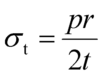
This effect could be explained by the thin-walled pressure vessel theory, which explains how the stress is affected by the radius of the vessel, as shown in eqn (1), where σt is the tangential stress in the vessel, p is the pressure inside the vessel, r is the radius, and t is the thickness of the walls.47 We assume the silicon and surrounding electrode matrix is a thin-walled pressure vessel, and that diffusion-induced stress is negligible, so all stress buildup is related to silicon expansion being constrained by the surrounding matrix.48 Assuming the volume expansion of a Si NP is the same with lithiation across particle sizes, then internal pressure should be similar, or scale with particle size. If we also assume that the thickness t of the surrounding electrode matrix coating is similar across all electrodes regardless of particle size, then only radius is varying with each electrode. Therefore, larger NPs, even if they are below the 150 nm limit for particle fracture, will still transmit more strain to the surrounding electrode matrix than smaller NPs. If this tangential stress exceeds the von Mises stress of the electrode matrix, then the volume expansion of the larger Si NP will cause mechanical damage to the electrode, even if it doesn't rupture the Si NP itself. This argument could also be applied to a thin SEI layer formed around a Si NP; if the thickness of the SEI layer does not vary with particle size, then larger particles will transmit more stress to the SEI shell, making it more likely to break the SEI.
 | (1) |
Fig. 3c shows SEM images of the 6, 14, and 27 nm electrode cross-sections at higher magnification. Pristine electrodes have a very densely packed structure, and electrodes with smaller particle sizes had pore sizes smaller than the resolution of the SEM. Though it is possible the nanoparticles form agglomerates during electrode drying and annealing steps, these agglomerates are not visible in the SEM images due to the closely-packed structure. After cycling, there is significant mechanical damage and increased porosity, as well as significant SEI build-up, that contributes to irreversible volume changes.
Using image segmentation, an estimate of the visible porosity of selected electrodes was calculated and plotted in Fig. 3d. Electrodes with particles smaller than 8 nm were hard to segment as the pore size of the electrode is likely below the resolution of the SEM. In general, electrodes with larger particles have slightly increased porosity, though even the largest-sized particle electrodes still have very dense microstructures (around 15% porosity, which correlates with previous estimates for similar electrodes).30
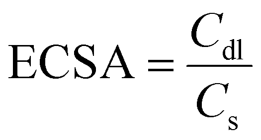
In porous electrodes, it is expected that smaller spherical particles would result in an electrode with more surface area, thus increasing the amount of irreversible side reactions. However, from Fig. 2, we do not see a significant difference in calendar aging in these electrodes, indicating that the very limited porosity of the electrodes might lower the actual surface area exposed to electrolyte. To measure this, electrochemical active surface area (ECSA) of the electrodes was quantified using cyclic voltammetry (CV) in symmetric blocking electrolyte cells using eqn (2), where Cdl is the double layer capacitance (measured using the symmetric cells with pristine silicon electrodes) and Cs is specific capacitance (3.7 μF cm−2 for silicon, measured with a symmetric cell with sputtered silicon thin films).36,37
 | (2) |
Fig. 4a shows an example of the CV curves from a blocking electrolyte symmetric cell; Fig. 4b shows the maximum and minimum currents at the cells’ initial open-circuit voltage fit to a line versus the scan rate. Fig. 4d plots the measured ECSA of each electrode using this method, showing no clear trend with particle size. Also plotted is an estimation of the surface area calculated assuming the Si NPs are isolated spheres, assuming a density of silicon to be 2.33 g cm−3, which predicts a much higher surface area than the measured ECSA. We do not expect the silicon particles to be isolated spheres, however, as they likely would have some overlap that would lower the effective surface area of the silicon. To model this surface area, electrode microstructures with 3, 9, 15 and 30 nm Si NPs were generated using a MATLAB-based microstructural modeling tool, MATBOX (see ESI Fig. S20 and S21† for further details).38,39 Examples of generated microstructures using this toolbox are shown in Fig. 4c. The resulting silicon-to-pore surface areas (with electrode porosities fixed to 20%, and assuming transverse anisotropy for the SWCNTs) are plotted in Fig. 4d, compared to the measured ECSA calculated from the symmetric cell CV results. As expected, the computational model predicts a lower surface area than the isolated spheres estimate, as there is significant overlap in a low porosity electrode. However, the measured ECSA is still several orders of magnitude lower than the computational results. This indicates that even the larger nanoparticles form electrodes so dense that the liquid electrolyte is unable to infiltrate throughout the electrode (see Table S4† for more discussion). As such, only the top surface of the electrode is in contact with the electrolyte, which explains why no significant difference in calendar aging was observed for different-sized particles despite higher surface-to-volume ratios for smaller spheres. Therefore, the Si NP dense electrode structure acts like a micron-thick layer, allowing for smaller NPs to be used without a penalty from additional side reactions due to increased surface-to-volume ratios.
 | ||
| Fig. 4 Electrode surface area calculations. (a) Example cyclic voltammetry results in a symmetric cell with a blocking electrolyte. (b) The minimum and maximum currents at open-circuit potential are fitted to a line versus scan rate. (c) Examples of microstructures numerically generated by MATBOX (with some particles removed to show nanotubes). (d) Electrochemically active surface area as a function of particle diameter, from the symmetric CV measurements, estimations from isolated spheres, and the microstructural model results. (e) Silicon-to-silicon contact area, calculated from the microstructural model, fit to an exponential decay. | ||
Due to the blocking conditions necessary for the ESCA measurement, electrodes that have been exposed to Li+ cannot be quantified (i.e. calendar aged or cycled samples). It is worth noting that electrodes that have been cycled more than the calendar aging cells (>40 cycles) might calendar age more aggressively than the results shown in Fig. 2, because of the mechanical damage to the electrode structure shown in Fig. 3. Therefore, it is imperative that the electrode structure is preserved as much as possible to realize the benefits of this dense microstructure.
From the microstructural model, the silicon-to-silicon contact area was calculated and shown in Fig. 4e, with an exponential fit. Like the silicon-to-pore surface area shown in Fig. 4b, the microstructural model predicts that smaller particle sizes would result in higher silicon-to-silicon connectivity. This could result in faster diffusion times, though galvanostatic intermittent titration technique (GITT) results (shown in ESI Fig. S4†) show no significant difference in diffusion coefficients with respect to particle size. This indicates that the limiting transport in these electrodes is likely solid-state diffusion of Li through Si, as these thin electrodes likely do not have ionic transport.
Electrode property correlations
To understand how the silicon NP size relates to performance and electrode properties, a linear correlation analysis was performed and is shown in Fig. 5. Each square represents a pair of electrode properties, with standard deviation error bars (if present) plotted, and each point is color-coded for particle size (larger particles are represented as lighter in color, consistent with other figures). The Pearson correlation coefficient (accounting for error) for each correlation is shown, and the statistical significance of that correlation was calculated (see the ESI and Table S5† for more details).49 If a correlation is significant, the square is shaded gray; a darker gray indicates greater significance. | ||
| Fig. 5 Linear correlation plots of particle size, electrochemically active surface area, silicon-to silicon connectivity, N/P ratio, electrode areal capacity, electrode specific capacity, cycle life, coulombic efficiency, calendar life, and impedance rise. Points are color-coded for particle size. For each pair, the Pearson correlation coefficient (accounting for standard deviations, if present) is displayed. The squares are shaded gray if the correlation is significant. The best fit line, including error, is shown for each square. Correlations exclude 3 and 4 nm electrode outliers. | ||
As the 3 and 4 nm electrodes performed consistently different than the other electrodes, possibly due to differences in electrode quality (as opposed to a fundamental difference in mechanics), the correlations in Fig. 5 only include electrodes with nanoparticles of 6 nm or greater. See Fig. S22† for correlation plots including all electrodes. As can be seen in Fig. 5, several correlations are statistically significant. This includes a correlation between particle diameter and silicon-to-silicon contact area, which is unsurprising as the silicon contact area follows an exponential decay with respect to diameter. Also as expected, areal and specific capacity are correlated.
There is also a correlation between diameter and electrode expansion after cycling. As stated before, this could be due to when the cycled samples were harvested from the coin cell (Fig. S19†). Nonetheless, this correlation between particle diameter and electrode volume expansion suggests that the main mechanism of capacity fade is related to the mechanical damage to the electrode matrix caused by the volumetric expansion of the Si NPs. More mechanical damage leads to more opportunities for electrolyte contact with the silicon, and potentially islands of disconnected, inactive material.
Particle diameter, cycle life, and coulombic efficiencies are all correlated with each other. This is supported from Fig. 1, which shows a clear trend in cyclability, coulombic efficiency, and particle size. The Si–Si specific contact interface is also strongly correlated with other metric (average absolute Pearson correlation coefficient = 0.44, surpassed by the particle diameter average at 0.51). For a given diameter, a high Si–Si specific contact interface implies less Si–pore interface, and therefore less surface available for parasitic reaction, and a higher emphasis on the need for a fast solid-state diffusion.
No significant correlations between calendar aging and impedance rise metrics exist. This is consistent with Fig. 2, which shows electrodes with particle sizes 6 nm and greater don't have an obvious connection between aging and particle diameter. This underscores the advantages of these dense electrodes, which protect the additional surface area from smaller Si NPs from electrolyte contact. Therefore, we do not have a trade-off between better cycle or calendar life performance. We also see no correlations with the N/P ratio and cycle or calendar aging parameters, indicating that the oversized cathode did not contribute to the cyclability or aging differences between silicon particle sizes.
These correlations elucidate why smaller Si NPs are key to enabling high-content silicon anodes that can reach key targets for electric vehicle batteries. This shows that the particle size of the silicon, even below the 150 nm threshold where silicon should not fracture, still greatly affects the performance of the battery, and that the microstructure of the anode can prevent additional irreversible losses due to more surface area. A second article further guides the choice of the particle size by correlating the optimal diameter with the SWCNT weight loading through a microstructure scale analysis.41
Conclusions
In summary, we made high silicon content anodes with ten different Si NP sizes. We tested these electrodes’ cycle and calendar aging performances. We found that the smaller Si NPs 6–12 nm in diameter are correlated with increased cycle life and higher coulombic efficiencies. There is no significant difference in calendar aging performance, despite more theoretical surface area for smaller particles, with average ASI rise of ∼3 Ω cm2 per month for particles 6 nm and greater, at 45 °C. Through microstructural characterization, we show that these Si NPs form a dense electrode with less than 15% visible porosity. This compact structure acts almost like a solid layer, and limits electrolyte contact with the silicon surface, which reduces SEI formation. Therefore, we can make high-silicon content electrodes with small nanoparticles to get the benefit of improved cycling performance without increasing the active surface area exposed to electrolyte. These promising results suggest that with careful optimization of Si NP electrodes, high-content Si electrodes could be a viable option for electric vehicle batteries that are competitive in cost and energy-density to traditional graphite anode batteries.Data availability
The data supporting this article have been included in the main text or as part of the ESI.†The analysis software MATBOX used to generate the compositional model is publicly available at: https://www.nrel.gov/transportation/matbox.html. This is included in the citations in the main text.
Conflicts of interest
There are no conflicts to declare.Acknowledgements
This work was authored by the National Renewable Energy Laboratory (NREL), operated by Alliance for Sustainable Energy, LLC, for the U.S. Department of Energy (DOE) under Contract No. DE-AC36-08GO28308. This research was supported by the U. S. Department of Energy, Vehicle Technologies Office (DOE-VTO) under the Silicon Consortium Project, directed by Nicolas Eidson, Carine Steinway, Thomas Do, and Brian Cunningham, and managed by Anthony Burrell. Thanks to Gabriel Veith, Taylor Thomas and Gabrielle Kliegle for experimental support. The views expressed in the article do not necessarily represent the views of the DOE or the U.S. Government. The U.S. Government retains and the publisher, by accepting the article for publication, acknowledges that the U.S. Government retains a nonexclusive, paid-up, irrevocable, worldwide license to publish or reproduce the published form of this work, or allow others to do so, for U.S. Government purposes.References
- Batteries – Vehicle Technologies Office [Internet]. Department of Energy, Office of Energy and Renewable Energy; available from: https://www.energy.gov/eere/vehicles/batteries.
- B. Cunningham, Silicon and Intermetallic Anode Portfolio Strategy Overview, Annual Merit Review, 2021 Search PubMed, (US Department of Energy).
- M. N. Obrovac and V. L. Chevrier, Alloy Negative Electrodes for Li-Ion Batteries, Chem. Rev., 2014, 114(23), 11444–11502 CrossRef CAS PubMed.
- C. Ballif, F. J. Haug, M. Boccard, P. J. Verlinden and G. Hahn, Status and perspectives of crystalline silicon photovoltaics in research and industry, Nat. Rev. Mater., 2022, 7(8), 597–616 CrossRef.
- J. K. Kearns in Single Crystals of Electronic Materials, ed. R. Fornari, Woodhead Publishing, Elsevier, 2019, pp. 5–56 Search PubMed.
- C. Stetson, Y. Yin, A. Norman, S. P. Harvey, M. Schnabel and C. Ban, et al., Evolution of solid electrolyte interphase and active material in the silicon wafer model system, J. Power Sources, 2021, 482, 228946 CrossRef CAS.
- J. E. Coyle, M. T. Brumbach, G. M. Veith and C. A. Apblett, Investigating the Chemical Reactivity of Lithium Silicate Model SEI Layers, J. Phys. Chem. C, 2020, 124(15), 8153–8161 CrossRef CAS.
- Y. Yin, E. Arca, L. Wang, G. Yang, M. Schnabel and L. Cao, et al., Nonpassivated Silicon Anode Surface, ACS Appl. Mater. Interfaces, 2020, 12(23), 26593–26600 CrossRef CAS PubMed.
- F. Wu, Y. Dong, Y. Su, C. Wei, T. Chen and W. Yan, et al., Benchmarking the Effect of Particle Size on Silicon Anode Materials for Lithium–Ion Batteries, Small, 2023, 19(42), 2301301 CrossRef CAS PubMed.
- X. Su, Q. Wu, J. Li, X. Xiao, A. Lott and W. Lu, et al., Silicon-Based Nanomaterials for Lithium- Ion Batteries: A Review, Adv. Energy Mater., 2013, 4(1), 1300882 Search PubMed.
- X. H. Liu, L. Zhong, S. Huang, S. X. Mao, T. Zhu and J. Y. Huang, Size-Dependent Fracture of Silicon Nanoparticles During Lithiation, ACS Nano, 2012, 6(2), 1522–1531 Search PubMed.
- Y. Li, S. Meyer, J. Lim, S. C. Lee, W. E. Gent and S. Marchesini, et al., Effects of Particle Size, Electronic Connectivity, and Incoherent Nanoscale Domains on the Sequence of Lithiation in LiFePO4 Porous Electrodes, Adv. Mater., 2015, 27(42), 6591–6597 CrossRef CAS PubMed.
- B. Orvananos, H. C. Yu, A. Abdellahi, R. Malik, C. P. Grey and G. Ceder, et al., Kinetics of Nanoparticle Interactions in Battery Electrodes, J. Electrochem. Soc., 2015, 162(6), A965–A973 CrossRef CAS.
- M. J. Loveridge, M. J. Lain, I. D. Johnson, A. Roberts, S. D. Beattie and R. Dashwood, et al., Towards High Capacity Li-ion Batteries Based on Silicon-Graphene Composite Anodes and Sub- micron V-doped LiFePO4 Cathodes, Sci. Rep., 2016, 6(1), 37787 CrossRef CAS PubMed.
- J. Newman and W. Tiedemann, Porous-electrode theory with battery applications, AIChE J., 1975, 21(1), 25–41 CrossRef CAS.
- A. M. Dreizler, N. Bohn, H. Geßwein, M. Müller, J. R. Binder and N. Wagner, et al., Investigation of the Influence of Nanostructured LiNi0.33Co0.33Mn0.33O2Lithium-Ion Battery Electrodes on Performance and Aging, J. Electrochem. Soc., 2018, 165(2), A273–A282 CrossRef CAS.
- M. D. Radin, S. Hy, M. Sina, C. Fang, H. Liu and J. Vinckeviciute, et al., Narrowing the Gap between Theoretical and Practical Capacities in Li-Ion Layered Oxide Cathode Materials, Adv. Energy Mater., 2017, 7(20), 1602888 CrossRef.
- A. C. Wagner, N. Bohn, H. Geßwein, M. Neumann, M. Osenberg and A. Hilger, et al., Hierarchical Structuring of NMC111-Cathode Materials in Lithium-Ion Batteries: An In-Depth Study on the Influence of Primary and Secondary Particle Sizes on Electrochemical Performance, ACS Appl. Energy Mater., 2020, 3(12), 12565–12574 CrossRef CAS.
- H. Zhong, D. Liu, X. Yuan, X. Xiong and K. Han, Advanced Micro/Nanostructure Silicon- Based Anode Materials for High-Energy Lithium-Ion Batteries: From Liquid- to Solid- State Batteries, Energy Fuels, 2024, 38, 7693–7732 CrossRef CAS.
- K. Feng, M. Li, W. Liu, A. G. Kashkooli, X. Xiao and M. Cai, et al., Silicon–Based Anodes for Lithium–Ion Batteries: From Fundamentals to Practical Applications, Small, 2018, 14(8), 1702737 CrossRef PubMed.
- G. Zhu, D. Chao, W. Xu, M. Wu and H. Zhang, Microscale Silicon-Based Anodes: Fundamental Understanding and Industrial Prospects for Practical High-Energy Lithium-Ion Batteries, ACS Nano, 2021, 15(10), 15567–15593 CrossRef CAS PubMed.
- T. N. Hung, F. Yao, M. R. Zamfir, C. Biswas, K. A. So and Y. H. Lee, et al., Highly Interconnected Si Nanowires for Improved Stability Li-Ion Battery Anodes, Adv. Energy Mater., 2011, 1(6), 1154–1161 Search PubMed.
- J. L. Dong, H. Lee, M. H. Ryou, G. B. Han, J. N. Lee and J. Song, et al., Electrospun Three- Dimensional Mesoporous Silicon Nanofibers as an Anode Material for High-Performance Lithium Secondary Batteries, ACS Appl. Mater. Interfaces, 2013, 5(22), 12005–12010 CrossRef PubMed.
- Y. Yao, M. T. McDowell, I. Ryu, H. Wu, N. Liu and L. Hu, et al., Interconnected Silicon Hollow Nanospheres for Lithium-Ion Battery Anodes with Long Cycle Life, Nano Lett., 2011, 11(7), 2949–2954 Search PubMed.
- Q. Xiao, M. Gu, H. Yang, B. Li, C. Zhang and Y. Liu, et al., Inward lithium-ion breathing of hierarchically porous silicon anodes, Nat. Commun., 2015, 6(1), 8844 CrossRef CAS PubMed.
- S. Ohara, J. Suzuki, K. Sekine and T. Takamura, A thin film silicon anode for Li-ion batteries having a very large specific capacity and long cycle life, J. Power Sources, 2004, 136(2), 303–306 CrossRef CAS.
- H. Jung, Amorphous silicon anode for lithium-ion rechargeable batteries, J. Power Sources, 2003, 115(2), 346–351 CrossRef CAS.
- M. Je, D. Han, J. Ryu and S. Park, Constructing Pure Si Anodes for Advanced Lithium Batteries, Acc. Chem. Res., 2023, 56(16), 2213–2224 CrossRef CAS PubMed.
- M. C. Schulze, G. M. Carroll, T. R. Martin, K. Sanchez-Rivera, F. Urias and N. R. Neale, Hydrophobic versus Hydrophilic Interfacial Coatings on Silicon Nanoparticles Teach Us How to Design the Solid Electrolyte Interphase in Silicon-Based Li-Ion Battery Anodes, ACS Appl. Energy Mater., 2021, 4(2), 1628–1636 CrossRef CAS.
- M. C. Schulze, F. Urias, N. S. Dutta, Z. Huey, J. Coyle and G. Teeter, et al., Control of nanoparticle dispersion, SEI composition, and electrode morphology enables long cycle life in high silicon content nanoparticle-based composite anodes for lithium-ion batteries, J. Mater. Chem. A, 2023, 11(10), 5257–5266 RSC.
- S. Jiang, B. Hu, R. Sahore, H. Liu, G. F. Pach and G. M. Carroll, et al., Tailoring the Surface of Silicon Nanoparticles for Enhanced Chemical and Electrochemical Stability for Li-Ion Batteries, ACS Appl. Energy Mater., 2019, 2(9), 6176–6183 CrossRef CAS.
- J. D. McBrayer, M. T. F. Rodrigues, M. C. Schulze, D. P. Abraham, C. A. Apblett and I. Bloom, et al., Calendar aging of silicon-containing batteries, Nat. Energy, 2021, 6(9), 866–872 CrossRef CAS.
- L. Mangolini, E. Thimsen and U. Kortshagen, High-Yield Plasma Synthesis of Luminescent Silicon Nanocrystals, Nano Lett., 2005, 5(4), 655–659 CrossRef CAS PubMed.
- L. M. Wheeler, N. C. Anderson, P. K. B. Palomaki, J. L. Blackburn, J. C. Johnson and N. R. Neale, Silyl Radical Abstraction in the Functionalization of Plasma-Synthesized Silicon Nanocrystals, Chem. Mater., 2015, 27(19), 6869–6878 Search PubMed.
- G. M. Carroll, M. C. Schulze, T. R. Martin, G. F. Pach, J. E. Coyle and G. Teeter, et al., SiO2 Is Wasted Space in Single-Nanometer-Scale Silicon Nanoparticle-Based Composite Anodes for Li- Ion Electrochemical Energy Storage, ACS Appl. Energy Mater., 2020, 3(11), 10993–11001 Search PubMed.
- R. Kumar, M. Singh and A. Soam, Study on electrochemical properties of silicon micro particles as electrode for supercapacitor application, Surf. Interfaces, 2020, 19, 100524 CrossRef CAS.
- D. M. Morales and M. Risch, Seven steps to reliable cyclic voltammetry measurements for the determination of double layer capacitance, J. Phys.: Energy, 2021, 3, 034013 CAS.
- F. L. E. Usseglio-Viretta, P. Patel, E. Bernhardt, A. Mistry, P. P. Mukherjee and J. Allen, et al., MATBOX: An Open-source Microstructure Analysis Toolbox for microstructure generation, segmentation, characterization, visualization, correlation, and meshing, SoftwareX, 2021, 17, 100915 Search PubMed.
- S. J. Cooper, A. Bertei, P. R. Shearing, J. A. Kilner and N. P. Brandon, TauFactor: An open-source application for calculating tortuosity factors from tomographic data, SoftwareX, 2016, 5, 203–210 CrossRef.
- NREL, MATBOX: Microstructure Analysis Toolbox [Internet]. Available from: https://www.nrel.gov/transportation/matbox.html.
- F. L. E. Usseglio-Viretta, J. I. Preimesberger, J. E. Coyle, Z. Huey, C. S. Jiang, J. H. Kim, N. R. Neale, G. M. Carroll and A. M. Colclasure, Maximizing Silicon Anode Material Utilization with Carbon Nanotubes Through Microstructure Scale Analysis [In progress].
- F. L. E. Usseglio-Viretta, A. M. Colclasure, A. R. Dunlop, S. E. Trask, A. N. Jansen and D. P. Abraham, et al., Carbon-Binder Weight Loading Optimization for Improved Lithium-Ion Battery Rate Capability, J. Electrochem. Soc., 2022, 169(7), 070519–070519 Search PubMed.
- A. Bezdek and W. Kuperburg, Dense packing of space with various convex solids, in Geometry - Intuitive, Discrete, and Convex, Springer, Berlin, 2013 Search PubMed.
- C. Song, P. Wang and H. A. Makse, A phase diagram for jammed matter, Nature, 2008, 453(7195), 629–632 Search PubMed.
- D. A. Rajon, P. W. Patton, A. P. Shah, C. J. Watchman and W. E. Bolch, Surface area overestimation within three–dimensional digital images and its consequence for skeletal dosimetry, Med. Phys., 2002, 29(5), 682–693 Search PubMed.
- Z. M. Konz, E. J. McShane and B. D. McCloskey, Detecting the Onset of Lithium Plating and Monitoring Fast Charging Performance with Voltage Relaxation, ACS Energy Lett., 2020, 5(6), 1750–1757 CrossRef CAS.
- C. T. Herakovich, Thin-Walled Pressure Vessels, in A Concise Introduction to Elastic Solids, Springer, 2017, pp. 77–81 Search PubMed.
- A. Verma, A. Singh and A. Colclasure, On the Impact of Mechanics on Electrochemistry of Lithium-Ion Battery Anodes, JOM, 2023, 76(3), 1171–1179 Search PubMed.
- D. P. Francis, J. S. C. Andrew and D. G. Gibson, How high can a correlation coefficient be? Effects of limited reproducibility of common cardiological measures, Int. J. Cardiol., 1999, 69(2), 185–189 CrossRef CAS PubMed.
Footnote |
| † Electronic supplementary information (ESI) available. See DOI: https://doi.org/10.1039/d4eb00020j |
| This journal is © The Royal Society of Chemistry 2025 |