
Modulation anisotropy of nanomaterials toward monolithic integrated polarization-sensitive photodetectors
Yuan
Pan†
,
Huiru
Sun†
,
Lingxuan
Ji
,
Xuanxuan
He
,
Wenzhe
Dong
and
Hongyu
Chen
 *
*
Guangdong Provincial Key Laboratory of Chip and Integration Technology, School of Electronic Science and Engineering (School of Microelectronics), Faculty of Engineering, South China Normal University, Foshan 528225, P.R. China. E-mail: chenhy@m.scnu.edu.cn
First published on 13th February 2025
Abstract
By virtue of the unique ability of providing additional information beyond light intensity and spectra, polarization-sensitive photodetectors could precisely identify targets in several concealed, camouflaged, and non-cooperative backgrounds, making them highly suitable for potential applications in remote sensing, astronomical detection, medical diagnosis, etc. Therefore, to provide a comprehensive design guideline for a wide range of interdisciplinary researchers, this review provides a general overview of state-of-the-art linear, circular, and full-Stokes polarization-sensitive photodetectors. In particular, from the perspectives of technological progress and the development of nanoscience, the detailed discussion focuses on strategies to simplify high-performance polarization-sensitive photodetectors, reducing their size and achieving a smaller volume. In addition, to lay a solid foundation for modulating the properties of future nanostructure-based polarization-sensitive photodetectors, insights into light–matter interactions in low-symmetry materials and asymmetric structures are provided here. Meanwhile, the corresponding opportunities and challenges in this research field are identified.
 Hongyu Chen | Hongyu Chen received her Ph.D. from the Changchun Institute of Optics, Fine Mechanics and Physics, Chinese Academy of Sciences, in 2014. Afterward, she worked as a postdoctoral fellow in the Department of Materials Science, Fudan University, China. Since then, she has worked as a lecturer in the Department of Physics, Harbin Institute of Technology, China. Currently, she is an associate professor at the School of Electronic Science and Engineering (School of Microelectronics), South China Normal University, China. Her current research interests include the design, fabrication, and exploration of novel properties of optoelectronic devices based on semiconductor and metallic materials, with a special focus on low-dimensional photodetectors. |
1. Introduction
During the past few decades, it has been witnessed that the booming photodetectors, functioning as “electronic eyes”, have transformed the way we understand the world. In particular, several special-function photodetectors not only allow us to “see” previously invisible substances (such as ultraviolet or infrared radiation), but also enable us to identify targets more precisely.1 Notably, based on the special ability to enhance the recognition of optical information dimensions from three dimensions (intensity, spectrum, and space) to seven dimensions (intensity, spectrum, space, polarization, polarization azimuth, polarization ellipticity, and rotation direction), polarization-sensitive photodetectors could further upgrade the capacity of photodetection to improve visual contrast and acuity.2 There is no doubt about the paramount significance of polarization-sensitive imaging techniques in fields such as remote sensing, environmental monitoring, astronomy, secure communications, medical diagnostics, autonomous navigation, and human–robot collaboration.3–7So far, most of the commercial polarization-sensitive photodetectors in terms of amplitude-, time-, local area-, and focal plane-resolved technological implementations have been realized using non-monolithic approaches, in which polarizers are positioned in front of photodetectors.8 However, under the impetus of Moore's law, the feature size of highly integrated electronic devices has shrunk toward several nanometers.9 Therefore, to realize a highly integrated polarization-sensitive photodetection system, it is essential to scale photodetectors down to the nanoscale. Nevertheless, conventional polarizers start to malfunction due to the optical diffraction limit when their size decreases to a sub-wavelength scale.10 Consequently, there is an urgent need to develop techniques to resolve these contradictions. Fortunately, as a new class of building blocks, several nanostructured materials with asymmetric structures exhibiting a special quantum confinement effect, surface effect, nonlinear optical effect, and dielectric confinement effect are explored for fabricating nanostructured monolithic polarization-sensitive photodetectors, which exhibit huge potential to resolve this convoluted issue.1,6,7,11,12 For instance, the application of nonlinear optical effects not only facilitates in-depth research into the anisotropic properties of 2D materials and the generation of circularly polarized light using chiral materials but also spurs the development of full-Stokes polarization-sensitive photodetectors based on metasurfaces.13–16 Moreover, nanoscale metallic and half-metallic materials exhibit fascinating optical properties, which can concentrate, route, and manipulate light at a sub-wavelength scale.9 Therefore, the potential applications of anisotropic nanostructured materials for fabricating monolithic polarization-sensitive photodetectors are truly impressive.
Up to now, extensive efforts have been made to explore the anisotropic optoelectronic properties of nanostructured materials and associated polarization-sensitive photodetectors, while a review of monolithic polarization-sensitive photodetectors involving potential materials and building blocks is still lacking. Herein, this review systematically demonstrates the current literature on photodetectors ranging from linear through circular to full-Stokes polarization-sensitive devices (Fig. 1). In particular, the polarization-sensitive photodetection technology is meticulously traced from complexity to simplicity, especially in the context of miniaturization and integration. Then, the light–matter interactions in low-symmetry materials as well as the design principles of polarization-sensitive photodetectors are described before outlining the challenges and opportunities in this area.
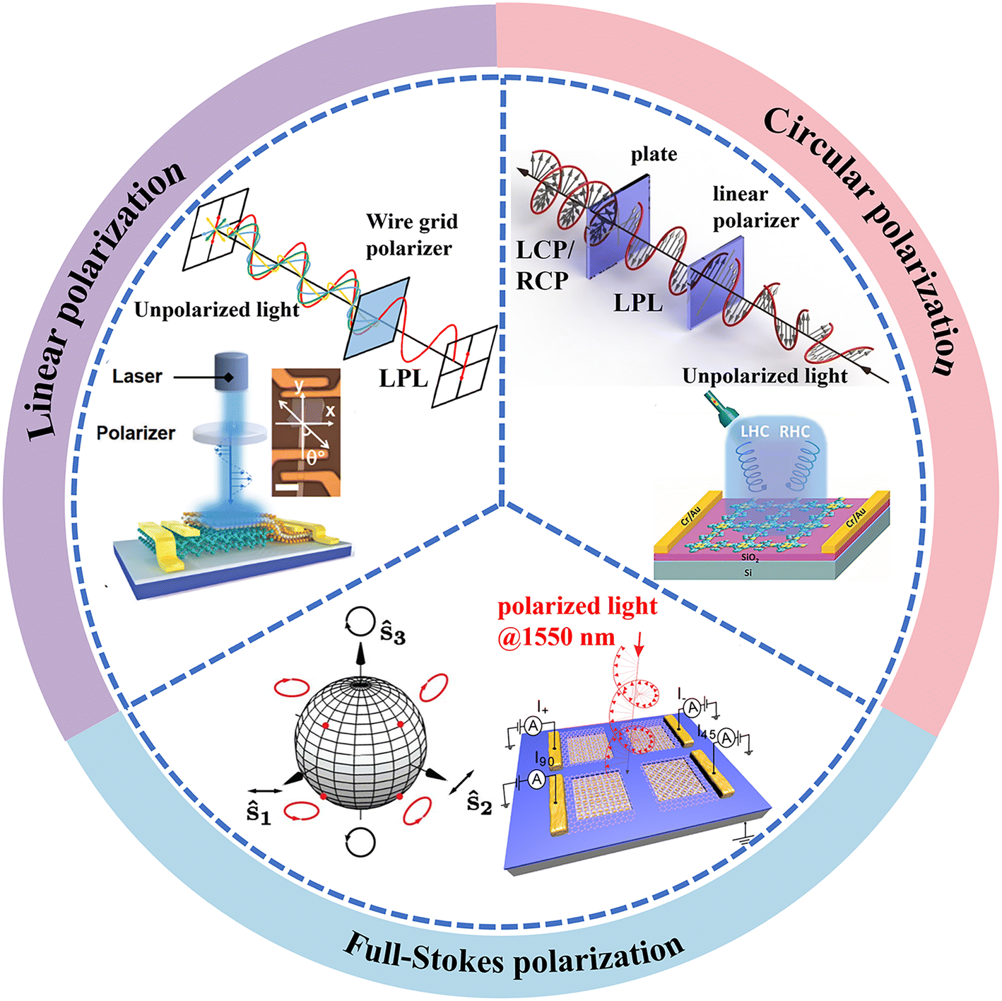 | ||
| Fig. 1 The main classifications of polarization-sensitive photodetectors: linear-,17 (copyright 2021, Royal Society of Chemistry) circular-,18 (copyright 2023, John Wiley and Sons) and full-Stokes polarization19,20 (copyright 2016, Optica Publishing Group and copyright 2020, American Chemical Society). | ||
2. Polarization-sensitive photodetectors
This section deeply discusses several core research trends in the field of polarization-sensitive photodetectors, covering linear-, circular-, and full-Stokes polarization-sensitive photodetectors. The classification of these photodetectors and their typical working principles are discussed in detail. The purpose of this section is to systematically review the research progress of these polarization-sensitive photodetector technologies and emphasize their important characteristics.2.1 Linear polarization-sensitive photodetectors
The characteristic of linearly polarized light is that its electric field vector oscillates in a plane and propagates along a straight line. The operation of linear polarization-sensitive photodetectors relies on the differences in the absorption or reflection of light with different polarization directions by materials. In addition to common photodetector parameters, the performance of linear polarization-sensitive photodetectors is particularly dependent on the polarized ratio (μ), which is the ability to respond to linearly polarized light.6,21,22
It is usually reflected in the ratio of the maximum and minimum photocurrent generated by the photodetector under differently polarized light. The higher the polarized ratio, the greater the extinction ratio of the device, and the stronger the ability to distinguish information differences.
 | ||
| Fig. 2 Linear polarization-sensitive photodetectors based on micro–nano structures and 1D materials. (a) Structure of a broadband tunable absorber with a plasmonic grating24 (copyright 2018, Springer Nature). (b) The schematic structure of the Au–MoS2 polarization-sensitive photodetectors25 (copyright 2020, John Wiley and Sons). (c) Schematic diagram showing the photodetector device fabricated from an aligned CNT film26 (copyright 2016, Springer Nature). (d) Photocurrent mapping measurement of the Au/Sb2S3/Au photodetector31 (copyright 2020, John Wiley and Sons). | ||
Likewise, 1D nanowires like ZnO, GaSb, and SnO2 are widely utilized in polarization-sensitive photodetection applications.28–30 For instance, high-quality Sb2S3 nanowires were synthesized by Zhao et al., who systematically investigated the optical, vibrational and photoelectron anisotropy of Sb2S3 nanowires (Fig. 2d).31 The photodetector based on a single Sb2S3 nanowire exhibits excellent polarization sensitivity in the broadband range from ultraviolet to near-infrared (360–1550 nm), and the maximum dichroism ratio reaches 2.54 (at 638 nm), achieving excellent linearly polarized photodetection. Nevertheless, the selection of 1D materials available for the fabrication of linearly polarized photodetectors is considerably limited, which is also detrimental to the future development of large-area arrays. This restricts the enhancement of photodetector performance and the expansion of their application range.
Fig. 3 summarizes some single 2D materials with anisotropic characteristics and superior performance. Xia et al. verified the anisotropy of crystal structure, carrier mobility, conductivity, light absorption and Raman scattering of BP (Fig. 3a).34 These anisotropic characteristics make BP provide new possibilities in the design of new optoelectronics and electronic devices, which is of great significance for promoting technological progress in related fields. However, the instability of BP in the air limits its further development, and researchers are still actively exploring better materials to replace it.34,43–45 For example, Zhang's group investigated the atomic configuration of ReSe2 nanosheets (Fig. 3b), utilizing angle-resolved Raman spectroscopy.42 They developed photodetectors with tunable bipolar polarization sensitivity based on highly anisotropic ReSe2 nanosheets with an obvious anisotropic optical response, demonstrating the polarization photodetection ability of ReSe2 nanosheets for linear light.41 ReS2, which has a crystal structure similar to that of ReSe2, has also been confirmed by Liu et al. to possess anisotropic properties and polarization detection capabilities. Additionally, GeSe (Fig. 3c),15 GeP (Fig. 3d),39 γ-InSe (Fig. 3e),46 and GeAs2 (Fig. 3f)47 have all been confirmed to exhibit anisotropic and polarization characteristics. These 2D materials, which demonstrate in-plane anisotropy, offer significant competitive value in the field of polarization-sensitive photodetectors.
 | ||
| Fig. 3 2D materials with anisotropy and linear polarization-sensitive photodetectors based on these materials. (a) Characterization of the thickness of black phosphorus and polarization-resolved infrared relative extinction spectra when light is polarized along the six directions34 (copyright 2014, Springer Nature). (b) Diagram of the crystal structure of ReSe2 and polarization-sensitive photodetectors based on ReSe2 nanosheets42 (copyright 2016, American Chemical Society). (c) Atomic structure of bulk GeSe from the side view and evolution of photocurrent plotted with probe polarization from 0° to 360° at Vd = 2 V (ref. 15) (copyright 2017, American Chemical Society). (d) Perspective view of few-layer GeP with a single layer and typical output curves along x- and y-directions under illumination39 (copyright 2018, John Wiley and Sons). (e) Top view of the γ-InSe nanosheet crystal structure and ARPRS and polarization-dependent SHG of the γ-InSe nanosheet46 (copyright 2022, American Chemical Society). (f) Perspective view of few-layer GeAs2 and schematic representation of the GeAs2 polarization-sensitive photodetector47 (copyright 2018, John Wiley and Sons). | ||
By constructing heterostructures and using a built-in electric field to separate photogenerated carriers, the anisotropy of photocurrent can be improved, thereby enhancing polarization sensitivity. In Fig. 4a, An et al. reported a high-performance self-powered polarization-sensitive imaging photodetector based on a fully depleted van der Waals heterostructure (top-MoSe2/GeSe/bottom-MoSe2).48 The full depletion of the intermediate layer GeSe significantly improves the separation efficiency and transmission speed of photogenerated carriers and achieves an excellent polarized ratio of up to 12.5, which is 3.5 times and 7 times that of MoSe2/GeSe and single GeSe polarized photodetectors, respectively. This method (energy-band engineering) is also the most commonly used to enhance the performance of polarization-sensitive photodetectors.4,17,49,50
 | ||
| Fig. 4 Structures to improve the performance of linear polarization-sensitive photodetectors. (a) Schematic diagram of the T-MoSe2/GeSe/B-MoSe2 van der Waals heterostructure device, along with the polarization sensitivity characterization of T-MoSe2/GeSe/B-MoSe2 photodetectors48 (copyright 2024, John Wiley and Sons). (b) Schematic diagram of the 1T′-MoTe2/WSe2 photovoltaic detector and calculated PR values as a function of gate voltage51 (copyright 2023, John Wiley and Sons). (c) Schematic illustration of the GeSe/MoS2 heterojunction with the P(VDF-TrFE) gate and photoresponse performance of the P(VDF-TrFE)-GeSe/MoS2 heterojunction in the visible region52 (copyright 2021, Springer Nature). (d) Schematic of a BP device with a bowtie antenna array and calculated absorption in BP, with and without bowtie structures, when illuminated along the armchair direction53 (copyright 2018, American Chemical Society). | ||
Another measure to improve the performance of the polarized photodetector is to control the gate voltage. A novel photodetector based on semimetallic 1T′-MoTe2 and the ambipolar semiconductor WSe2 with excellent polarization sensitivity and gate-tunable optoelectronic reverse characteristics was introduced by Wang et al. (Fig. 4b).51 The photodetector is capable of capturing high-resolution imaging in complex environments, with a polarized ratio that can approximately reach 30. By changing the polarized angle of the incident light, the sign reversal of the polarized photocurrent can also be observed, which allows for a possible dynamic range of polarized ratios from 1 to +∞ and from −∞ to −1.
In addition, by finely adjusting the polarization state of ferroelectric materials, the electronic properties of low-dimensional van der Waals materials can be optimized to achieve directional improvement of polarized photodetection performance. As shown in Fig. 4c, Chen et al. proposed a new type of van der Waals heterojunction device,52 which relies on ferroelectric polarization control technology, by integrating a vertical heterojunction composed of GeSe and MoS2 and a ferroelectric polymer based on P(VDF-TrFE).
Another method involves tuning the resonance frequency of surface plasmons through metal nanostructures, thereby regulating the polarization characteristics of light. Venuthurumilli et al. introduced an alternative method to enhance polarization sensitivity by employing two plasmonic structures—bowtie antennas and bowtie apertures—to improve the optical response of BP-based photodetectors (Fig. 4d).53 The bowtie antenna leverages localized surface plasmon resonance to boost light absorption, predominantly in the armchair direction where absorption is more pronounced. The bowtie aperture structure, on the other hand, is designed to increase the absorption ratio of BP to light in different polarization directions, thus enhancing polarization selectivity. These methods significantly promote the design and performance optimization of polarization-sensitive photodetectors and establish a solid theoretical and practical foundation for the future development of photodetection technology.
Linear polarization-sensitive photodetectors are crucial for polarized imaging, optical communication, and biomedical fields, but their further development is limited by technical challenges, such as the complexity of monolithic integration, cost, and alignment issues, which restrict the miniaturization and integration of the photodetectors. Moreover, although research has made progress in the integration of large-area polarization-sensitive devices, there is still a need to address the orderliness of molecular stacking structures and the consistency of orientation. Enhancing the polarized ratio of polarization-sensitive photodetectors is also a technical challenge that requires optimization of the absorption or reflection characteristics of differently polarized light through the anisotropy of materials and structural design.
2.2 Circular polarization-sensitive photodetectors
Circular polarization is a special case of elliptical polarization, where the two electric field components have a phase difference of 90 degrees and equal amplitudes.54 Along the propagation direction, the endpoint trajectory of the electric field vector forms a circle. The electric field vector of clockwise rotation (commonly expressed as σ+) is right-handed circularly polarized light (RCP), and the electric field vector of counterclockwise rotation (commonly expressed as σ−) is left-handed circularly polarized light (LCP).55,56 The working principle of the circular polarization-sensitive photodetectors is mainly based on the difference in the absorption characteristics of the material to differently polarized light. Specifically, LCP and RCP may excite different photoelectric responses. The technology of circular polarization-sensitive photodetectors primarily relies on key mechanisms including optical chiral absorption characteristics, the circular photogalvanic effect (CPGE), the inverse spin Hall effect (ISHE), and spin-dependent recombination (SDR).57 This chapter will elaborate on the working principles and applications of circular polarization-sensitive photodetection based on the aforementioned structures.CD is usually expressed by ellipticity (Φ):62

CD spectroscopy is a technique widely used to identify chiral substances based on the difference in the absorption of LCP and RCP by molecules. The CD spectra of chiral materials usually show signal peaks (positive or negative peaks) at certain wavelengths.63 Achiral samples or racemic mixtures usually show flat spectra because there is no absorption difference for circularly polarized light.64 When a chiral semiconductor material is used as the active layer of the photodetector, photocurrent signals of different sizes are generated due to its differential absorption of RCP and LCP, which are quantified by the dissymmetry or g-factor (denoted as glum). This factor is a key parameter for evaluating the quality of chiral materials with CPL properties.65 In the experiment, glum can be expressed by the following formula:

Metamaterials, a collection of 3D periodic sub-wavelength unit structures, significantly enhance the ability to control light waves, making it possible to achieve precise modulation of light waves in a changing environment. These materials can finely manipulate the phase, amplitude and polarization of light waves at the sub-wavelength scale. A metasurface, as a 2D derivative of metamaterials, is an artificial micro–nano structure. Through sub-wavelength phase control, it can accurately control the propagation of light waves and achieve comprehensive polarization analysis. Compared with the electromagnetic wave control ability of metamaterials in 3D space, metasurfaces achieve fine control of electromagnetic waves in a 2D plane.57,66 Similar to linear polarization-sensitive photodetectors, early circular polarization-sensitive photodetectors are often based on the combination of chiral metasurfaces and photodetectors. Circularly polarized light can be effectively detected by using the difference in transmittance between LCP and RCP. Wei Li et al. proposed an ultra-compact circular polarization-sensitive photodetector based on chiral plasmonic metamaterials and hot electron injection.67 The structure is shown in Fig. 5a. They achieve a circular dichroism ratio of up to 0.72 by adjusting the size and angle of the metasurface array elements. Although chiral optical effects can be reproduced by combining metasurfaces or optical elements (such as quarter-wave plates), optical elements reduce efficiency and metasurfaces increase the complexity of the system and often increase costs.68 With the vigorous development of the field of chiral materials, researchers are increasingly aware of their potential for effective detection of circularly polarized light.
 | ||
| Fig. 5 Circular polarization-sensitive photodetectors based on chiral characteristics. (a) Schematic of the chiral metamaterial and the CPL photodetector67 (copyright 2015, Springer Nature). (b) Molecular structure and device architecture of the circularly polarized photo-detecting helicene OFETs71 (copyright 2013, Springer Nature). (c) Highly luminescent CPL emitters featuring a double T-helix extension and single-crystal structures of rac-572 (copyright 2024, American Chemical Society). (d) The crystal structures of our chiral perovskites and the device structure of the (R- and S-α-PEA)PbI3 film photodetector74 (copyright 2019, Springer Nature). (e) Schematic illustration of different circularly polarized lights passing through the twisted 2D material and the orientation of the top and bottom BP crystals76 (copyright 2023, American Chemical Society). | ||
Chirality refers to the property that an object cannot completely coincide with its mirror image, which is a key feature of these materials, including small molecules, polymers, organic crystals and perovskites.69,70 Chiral materials can not only adapt to a variety of nanostructures (structures including 0D hybridization, 1D nanowires, and 2D films), but also meet specific application requirements.6 Moreover, the absorption coefficients of RCP and LCP are inherently different, and the effective detection of circularly polarized light can be realized by utilizing this absorption difference. Ying Yang et al. used a helicene—a helically shaped chiral semiconducting molecule71—whose chiral structure causes a difference of about one order of magnitude in the absorption coefficients for RCP and LCP to prepare a circularly polarization-sensitive photodetector that utilizes chiral organic field-effect transistors (Fig. 5b). The transistor is highly sensitive to circularly polarized light and can detect even weak light signals effectively. It features a fast response time to light and an adjustable optical band gap, which is highly valuable for applications requiring high-sensitivity photodetection.
With the progress in the field of chiral materials, it has become a productive direction to explore the interaction between a helical structure and a π-conjugated structure. Not only are these structural extensions interconnected at multiple levels, but they also determine the chiral optical and electronic properties of the material. The periodicity and directionality of the helical structure can influence the transport and recombination of electrons within the π-conjugated system, thereby altering the material's absorption and emission properties with respect to circularly polarized light. This relationship between structural and electronic properties offers a theoretical foundation for designing molecules and materials with targeted chiral responses. The helical structure can enhance the chirality of the molecule, and the extension of the π-conjugated structure can further amplify and transfer this chirality. For example, Liu et al. developed a new type of double π-helical chiral molecular system fusing a perylene diimide unit (PDI) with a cyclooctatetraene unit (COT).72 They found that with the extension of the length of the chiral helical chain, the chiral optical properties were significantly enhanced, indicating that the combination of the helical structure and the π-conjugated structure played an important role in chiral transfer and amplification (Fig. 5c). A. Ishii et al. constructed a 1D perovskite structure by incorporating chiral cations (NEA+) that influence the helicity of the (PbI6)4− chains in the perovskite.73 This structure exhibits a strong CD signal of more than 3000 mdeg due to its spiral shape, with a high anisotropy factor of 0.04. The CPL detector utilizing this 1D perovskite structure successfully achieved an exceptional polarized discrimination ratio of 25.4.
In addition, by integrating chiral molecules into perovskite structures, the inherent chirality of these molecules can be used to enhance the sensitivity of materials to circularly polarized light, which is an important supplement to traditional inorganic semiconductor materials. The Chen group introduced a hybrid perovskite, (α-PEA) PbI3, integrating chiral α-phenylethylamine (α-PEA) with lead iodide (PbI3)74 (Fig. 5d). This material synergizes the CPL-sensitive absorption of chiral organics with the charge transport efficiency of inorganics.
In addition to the above materials and structures, 2D materials with chiral structures can also serve as ideal materials for chiral optoelectronic devices. Niu et al. explored how chirality affects 2D tellurium's (Te) response to circularly polarized light in field-effect transistors.75 They found that both the longitudinal circular photogalvanic effect (CPGE) and the circular photovoltaic effect (CPVE) depend on Te's chiral crystal structure. These effects make 2D Te a promising material for chirality-dependent optoelectronics. The study also shows that by adjusting the back-gate voltage, one can control the chiral properties and photocurrent response in 2D Te. In Fig. 5e, Wang et al. demonstrated that the chirality of these materials can be significantly adjusted by varying the twist angle between layers.76 This tunability, influenced by anisotropy and band structure, extends across the visible to infrared spectrum. The potential for spin-selective information transformation highlights their promise in spintronics, polarization optics, and nano-optoelectronics.
Significant progress has been made in elucidating the CPGE, especially in understanding the basic mechanism of photoexcited spin current. For example, in semiconductor heterostructures, the spin–orbit interaction associated with the Rashba effect drives the CPGE, while in topological Weyl semimetals, the interplay between the Berry phase and the Pauli blocking effect governs the selection of electron momentum. In 2D transition metal dichalcogenides (TMDCs), the valley polarization currents are excited by circularly polarized light.75,77,80–82 These insights not only enhance our understanding of the CPGE, but also pave the way for innovative electronic device architectures based on spin and valley degrees of freedom. Duan et al. realized the Berry curvature dipole (BCD) generated on the asymmetric heterogeneous interface of semiconductors and its application in helicity-to-spin conversion.83 They formed a WSe2/SiP (Fig. 6a) heterogeneous interface by stacking van der Waals monolayer materials with different lattice symmetries, breaking the rotational symmetry in the material, realizing the symmetry breaking of the interface crystal structure and the artificial modification of the energy band structure, and using their symmetry mismatch to induce the BCD. By changing the energy of the incident light and the gate voltage, the spin photocurrent at the heterogeneous interface can be regulated. The non-linear effect of Weyl semimetals is a unique phenomenon in topological materials. Ma et al., for the first time, observed a huge multiphoton response in type II Weyl semimetals.84 The experimental diagram is shown in Fig. 6b. The Berry curvature divergence at the Weyl node is the key factor that causes TaIrTe4 to produce a huge photocurrent response in the mid-infrared band. This divergence is similar to the magnetic monopole in the momentum space, and its sign determines the chirality. Not only is the nonlinear response of photocurrent observed, but the anisotropic and circularly polarized photocurrent effects are found also in different crystal directions. Moreover, Ni et al. mainly studied the longitudinal circularly polarized photocurrent effect generated by circularly polarized light excitation in chiral multi-fold half-metal CoSi.85 Through terahertz emission spectroscopy, a huge longitudinal photocurrent of about 550 μA V−2 was observed at a specific energy, and it was proved to be derived from topological band crossing. In addition, in TMDs such as MoS2, the valley polarization current generated by circularly polarized light is also an important manifestation of the CPGE. Valleytronics aims to increase the degree of freedom of optoelectronic devices by using valley degeneracy in the semiconductor energy band. Eginligil et al. found that monolayer MoS2, as a new valley electron material, exhibits significant valley polarization characteristics in photoluminescence, as revealed in Fig. 6c.86 By adjusting the polarized angle of the laser, they explored the correlation between the photocurrent and the polarized angle of the light, thus confirming the feasibility of controlling the spin–valley coupling current by precisely controlling the polarization of the light.
 | ||
| Fig. 6 Circular polarization-sensitive photodetectors based on the CPGE, ISHE and SDR. (a) Schematic figure for generation of the spin photocurrent for the WSe2/SiP device with incident light normal to the heterointerface83 (copyright 2023, Springer Nature). (b) Schematic diagram of the polarization-resolved scanning photocurrent measurement setup84 (copyright 2019, Springer Nature). (c) Band diagram of K and −K valleys of MoS2 and photocurrent generation86 (copyright 2015, Springer Nature). (d) A schematic illustration of the Pt/GaAs hybrid structure used in this study87 (copyright 2010, AIP Publishing). (e) Schematic diagram depicting the creation of a spin current induced by the intensity gradient of the Gaussian beam, subsequently converting into the circulating charge current91 (copyright 2024, Springer Nature). (f) Sketch of the experimental configuration used to simultaneously measure the photoluminescence (PL) and the PC93 (copyright 2021, John Wiley and Sons). | ||
K. Ando et al. used a Pt/GaAs hybrid structure for experiments (Fig. 6d).87 Within the GaAs layer, the absorption of circularly polarized light, in line with optical selection rules, gives rise to spin-polarized electrons in the conduction band, effectively translating the circularly polarized information of light into electron spin polarization. These spin-polarized electrons are then injected into the Pt layer as a pure spin current, facilitated by the Pt/GaAs interface. The robust spin–orbit coupling inherent to Pt materials enables the conversion of these injected pure spin currents into electric potential or electromotive force (EMF) through the ISHE. This phenomenon harnesses the spin–orbit interaction to encode spin information into electrical signals, offering a novel perspective on the design and material selection for photodetectors, which is pivotal for enhancing the efficiency of photoelectric effects. Khamari et al. presented a spin-optoelectronic detector that harnesses the ISHE in an Au/InP hybrid structure to concurrently measure the degree of circular polarization and the intensity of a laser beam.90 This device, integrating dual detectors on a single chip, leverages the ISHE for polarization assessment and the photovoltaic effect for intensity, operating without crosstalk. It offers rapid response, compactness, and integrability, advancing photonic and optical communication applications. In centrosymmetric materials, due to the existence of global inversion symmetry, hidden spin polarization is usually difficult to convert into spin current. In the work of Wang et al.,91 a spatially-varying circularly polarized light beam is normally incident on the centrosymmetric TMD semiconductor without an applied electric field. The spatial variation of the beam breaks the inversion symmetry of the system, as illustrated in Fig. 6e. By altering the electrode configuration, illumination position, and spot size, spin-polarized circularly polarized photocurrent was observed in multilayer 2H-MoTe2, 2H-MoS2, and 2H-WSe2.
Among them, GaAsN (this is a class of semiconductors based on GaAs, with a small amount of nitrogen (N) elements incorporated), due to its unique band structure, shows significant advantages in photodetector applications.93 The introduction of GaAsN materials can significantly enhance the sensitivity of photodetectors to circularly polarized light, which is difficult to achieve with traditional non-chiral III–V or IV–VI semiconductor materials. The performance enhancement achieved by GaAsN is mainly attributed to its spin-dependent recombination mechanism. This mechanism allows GaAsN materials to electrically measure the polarization state of light at room temperature, which not only simplifies the complexity of the system but also promotes the miniaturization and integration development of photodetectors.94,95 In Fig. 6f, Joshya et al. fabricated a GaAsN-based chiral photodetector capable of determining light polarization and intensity through conductivity measurements.93 They leveraged the chiral photoconductivity effect of the GaAsN epitaxial layer, which is influenced by spin-dependent recombination and spin-polarized defects. The researchers demonstrated that by manipulating the spin polarization of conduction band electrons, the material's conductivity could be controlled. Furthermore, they showed that applying an external magnetic field could adjust the hyperfine interaction and the Zeeman effect, thereby modulating the material's response to circularly polarized light (RCP or LCP). Ibarra-Sierra et al. prepared a novel spin-optoelectronic device that translates light's polarization into electrical signals via spin-dependent recombination and hyperfine interaction.96 In GaAs1−xNx, spin-polarized electrons and holes, excited by circularly polarized light, interact with Ga2+ centers, prolonging the lifetime of electrons with certain spin orientations while rapidly recombining others. This results in a buildup of spin-polarized electrons. The hyperfine interaction with the Ga2+ center's bound electrons and nucleus produces an Overhauser-like field under an external magnetic field, which differentially responds to the chirality of circularly polarized light, allowing the device to identify the light's chirality.
The development of circular polarization-sensitive photodetectors has been facilitated by a profound understanding of the physical mechanisms of optical absorption, CPGE, ISHE, and SDR. These technological breakthroughs have not only enhanced the performance and sensitivity of the photodetectors but also expanded their application prospects in fields such as optical imaging, optical communication, and quantum information processing. Despite facing technical challenges such as material property limitations, weak photocurrent, fabrication difficulties, and lattice mismatch issues, future development directions will focus on the development of new chiral semiconductor materials, exploration of new photoelectric mechanisms that directly respond to the spin of photons, optimization of artificial nanostructures, and the development of heterojunction devices, aiming to achieve higher-performance direct detection of circularly polarized light and broader applications.
2.3 Full-Stokes polarization-sensitive photodetectors
Full-Stokes polarization is an analytical method used to describe the polarization state of light by using Stokes parameters, which enables complete characterization of the polarization characteristics of any polarized light.19,20,97 The Stokes parameters are a set of four scalar values,19,98 which can be expressed as S = (S0, S1, S2, S3)T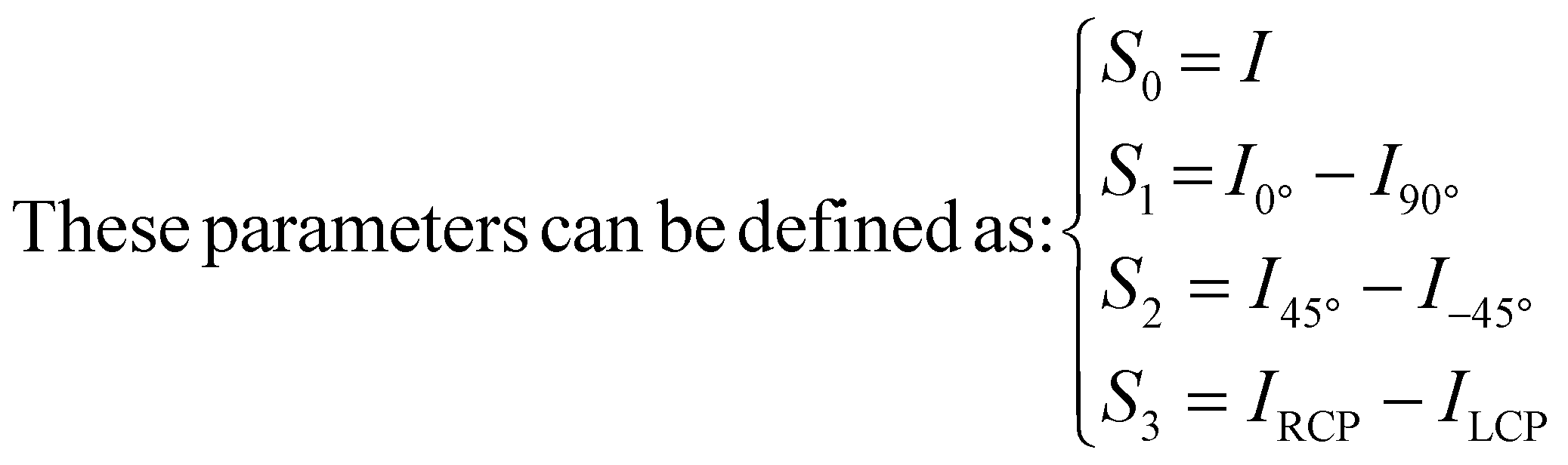
Here, the parameter S0 represents the total intensity of the light wave, summing intensities across all polarization directions, and is a scalar indicating the light wave's total energy independent of the polarization direction. S1 denotes the intensity difference between horizontally and vertically polarized light components. A positive S1 indicates stronger horizontal polarization, a negative suggests stronger vertical polarization, and zero implies equal intensities, suggesting non-polarized or circularly polarized light. S2 describes the intensity difference between light polarized at +45° and −45°. A positive S2 indicates stronger +45° polarization, a negative suggests stronger −45° polarization, and zero indicates equal intensities in both directions. S3 represents the intensity difference between RCP and LCP. A positive S3 indicates stronger right-handed polarization, a negative indicates stronger left-handed polarization, and zero signifies the absence of circular polarization or equal intensities of both components. Through the description of the unit vector, all possible polarization states can be geometrically expressed as a point on the unit ball, which is called the Poincaré sphere. Its three coordinate axes correspond to the three parameters of S1, S2, and S3, respectively. The surface of the ball can represent all fully polarized light, and the interior of the ball represents incompletely polarized light, while natural light is at the origin.
The Stokes vector is composed of four parameters, which provide a theoretical basis for the comprehensive characterization of polarized light. It delineates various polarized modes, including linear, circular, and their complex combinations, with detailed precision.19,99 Accurate measurement of these parameters allows for a detailed quantitative analysis of polarized light, revealing the underlying physical mechanisms. Developing photonic materials that are highly sensitive to both linear and circular polarization is crucial for constructing high-performance Stokes photodetectors. Such materials are essential for the accurate detection of polarized light. The full-Stokes polarization measurement technology, as an advanced analytical tool, significantly enhances our understanding of subtle differences in polarized light characteristics. It offers a comprehensive analysis of the polarization state and elucidates the polarization effects during light–matter interactions, providing valuable information for polarization research.
In the early stages of technological development, photodetectors mainly rely on traditional time-resolved measurement techniques. In order to capture the complete polarization state of light, at least four independent measurements are needed to determine the Stokes parameters of incident light. Rubin et al. from Harvard University developed a novel sub-wavelength diffraction grating for precise polarization control at visible frequencies.103 The grating, depicted in Fig. 7a, consists of anisotropic nanostructures that enable dynamic light polarization. By coupling with an imaging lens and sensor, it captures four diffraction orders, each filtered by different polarizers on the metasurface. A pixel-wise analysis of these images allows for the reconstruction of the four Stokes parameters of the scene. However, the method's reliance on time-sharing technology limits its speed, making it unsuitable for real-time polarization analysis of dynamic scenes. Then, different from the above time-resolved measurement, Zhang et al. have developed a pixel-based metasurface on an insulating silicon wafer for full-Stokes vector polarized photodetection in the near-infrared spectrum (Fig. 7b).104 The design integrates a ‘Z’-shaped circular polarizer with three linear polarizers, enabling simultaneous photodetection of linear and circular polarization states. This approach is compatible with semiconductor manufacturing, advancing on-chip polarized photodetection and polarized imaging technology. In addition, as illustrated in Fig. 7c, Zuo et al. have introduced a biomimetic full-Stokes polarized imaging sensor utilizing metasurface on-chip integration.102 A layer of a silicon metasurface that produces optical birefringence is stacked with a layer of a high-performance linearly polarized photodetection metasurface to achieve high-performance circularly polarized photodetection. Notably, the polarized extinction ratio of the biomimetic circular polarizer shows insensitivity to the incident angle, which ensures the high-precision polarized measurement capability of the sensor in a large field of view. This metasurface-based technology excels in imaging speed, integration, accuracy, and compatibility with standard semiconductor processes, providing a promising direction for future optical imaging advancements.
 | ||
| Fig. 7 Full-Stokes polarization-sensitive photodetectors based on metamaterials and metasurfaces. (a) Matrix gratings for arbitrary parallel polarization analysis103 (copyright 2019, The American Association for the Advancement of Science). (b) Schematic of the setup for near-infrared full-Stokes photodetection104 (copyright 2021, Optica Publishing Group). (c) CMOS integrated full-Stokes polarimetric imager with dual operation wavelengths102 (copyright 2023, Springer Nature). (d) Design architecture of a full-Stokes photodetector based on chiral plasmonic metamaterials57 (copyright 2022, Springer Nature). | ||
In addition, researchers have discovered that it is possible to use metamaterials to achieve full-Stokes polarization-sensitive photodetection. Dai et al. have developed a novel on-chip mid-infrared photodetector for full-Stokes polarization photodetection (Fig. 7d).57 This design employs chiral plasmonic metamaterials to selectively absorb light with specific polarizations, converting this absorption into electrical signals through the photoelectric thermoelectric effect. The polarization sensitivity is tunable by adjusting the chiral metamaterials’ spatial and geometric attributes, enabling the photodetection of both linear and circular polarization. The presented compact chip design is conducive to integrated polarized measurements in miniaturized optoelectronic systems. The photodetector's operation is not limited by the band gap of its active material, enhancing its application potential in different wavelength regions.
The ongoing interest in metamaterials and metasurfaces is expanding, particularly for their potential in creating compact, full-Stokes polarization-sensitive photodetectors that are easily integrated into smaller systems, aligning with the demand for miniaturization in modern optical devices.13,14,105 As on-chip integrated photodetector technology advances, simplifying the manufacturing process and achieving miniaturization of these photodetectors are crucial. Researchers are now leveraging the intrinsic properties and chiral control of low-dimensional materials for full-Stokes photodetection, marking a significant shift from metamaterial-based to low-dimensional material-based photodetectors and offering a new pathway to enhance photodetection performance.106–108
 | ||
| Fig. 8 Full-Stokes polarization-sensitive photodetectors based on low-dimensional materials. (a) Crystal structure and device architecture of a Stokes-parameter photodetector106 (copyright 2021, American Chemical Society). (b) Schematic diagram of a chiral perovskite-based photodetector and schematic diagrams of perovskite films with different imprinted area ratios109 (copyright 2024, John Wiley and Sons). (c) Full-Stokes polarimetric measurements and schematic of the setup for the polarization-resolved photocurrent measurement107 (copyright 2021, John Wiley and Sons). (d) Polarization states of incident light, described by Stokes parameters and drawn on the Poincaré sphere and schematic of the TDBG photodetector111 (copyright 2022, Springer Nature). | ||
In addition, the full-Stokes polarization-sensitive photodetectors prepared with low-dimensional materials can directly use the intrinsic characteristics of the material to perceive the polarized light, which is more conducive to achieving highly integrated devices and reducing production costs. It is an important research direction for the future development of full-Stokes polarized photodetectors. First, as shown in Fig. 8c, this review reports a full-Stokes polarimeter based on chiral perovskite materials, which can fully analyze the polarization state of light.107 The authors successfully constructed an integrated full-Stokes polarimeter using the optical anisotropy and response characteristics to circularly polarized light of chiral 2D perovskite materials (S- and R-MBA)2PbI4 (MBA = C6H5C2H4NH3). The device can accurately distinguish various types of polarized light, including linearly polarized light and circularly polarized light, without additional filters. Similar phenomena were also observed by Zhao et al., who recently constructed an innovative full-Stokes polarized photodetector with chiral 2D/quasi-2D perovskite heterojunction nanowire arrays.110 The work skillfully constructed a built-in electric field and utilized the anisotropy of the material to achieve high sensitivity photodetection of circularly polarized and linearly polarized light.
Moreover, similar to the previous circular polarization-sensitive photodetectors in this review, 2D materials can achieve polarized photodetection with different capabilities through twisted layers. Ma et al. employed the tunable mid-infrared bulk photovoltaic effect (BPVE) in twisted bilayer graphene (TDBG) combined with a convolutional neural network (CNN) to achieve full-Stokes polarimetry (Fig. 8d).111 The photovoltage mappings (Vph) produced by the TDBG device encode the polarization state and wavelength of incident light. Through training, the CNN can parse these mappings to extract the complete Stokes parameters and incident light wavelength from a single device. This capability enables simultaneous polarization and wavelength photodetection, essential for comprehensive full-Stokes analysis.
Full-Stokes polarization-sensitive photodetectors are evolving towards greater integration, real-time capabilities, and high sensitivity, enabling a comprehensive description of the polarization state of light and finding broad applications in fields such as autonomous driving and machine vision. Currently, these photodetectors face challenges including manufacturing complexity and measurement accuracy issues. Future research will focus on improving the measurement speed, wavelength compatibility, and reducing costs and size for better integration into existing systems. Additionally, the application of new materials and low-dimensional materials will pave new ways to enhance polarization-sensitive photodetection performance.
3. Summary and outlook
In this review, a comprehensive history and recent advances in linear, circular, and full-Stokes polarization-sensitive photodetectors are demonstrated. Table 1 summarizes the parameters and performance indicators of these three kinds of photodetectors. Obviously, as appealing platforms, several asymmetric or chiral nanostructured materials with a number of intriguing nonlinear photoelectric properties have established themselves as versatile building blocks in novel monolithic integration polarization-sensitive photodetectors. These materials not only enhance the performance of the photodetectors through alterations in their crystal structure and geometry but also enable the monitoring of multidimensional information, including light intensity, wavelength, polarization, phase, and even angular momentum, by modulating the anisotropy of the nanomaterials. Notably, full-Stokes polarimetry can be achieved using surface plasmon resonance metasurfaces, further expanding the capabilities of these photodetectors as appealing platforms.100,112| Device | Wavelength (nm) | Voltage (V) | Responsivity (mA W−1) | Detectivity (Jones) | Anisotropy (Imax/Imin) | Ref. | |
|---|---|---|---|---|---|---|---|
| Linear | MoS2/Au | 660 | 0 | 26![[thin space (1/6-em)]](https://www.rsc.org/images/entities/char_2009.gif) 000 000 |
1.45 | 25 | |
| Sb2S3 | 638 | 2 | 343.4 | 2.54 | 31 | ||
| γ-InSe | 405 | 1 | 127000 |
2.73 × 10¹¹ | 2.07 | 46 | |
| ReSe2 | 633 | 1 | 42 | ||||
| GeSe | 532 | 2 | 4250 | 1.09 | 15 | ||
| 638 | 2 | 1.44 | |||||
| 808 | 2 | 2.16 | |||||
| GeAs2 | 532 | 1 | 2 | 47 | |||
| GeP | 532 | 0.1 | 3110 | 1.83 | 39 | ||
| PdSe2 | 532 | 1 | 3.5 | 1.9 | 116 | ||
| SiAs | 514.5 | 2 | 5.3 | 40 | |||
| 325 | 2 | 2.3 | |||||
| BP/plasmonics | 1550 | 100 mV | 14.2 | 2.91 × 10¹³ | 8.7 | 53 | |
| Te/MoSe2 | 405 | 0 | 2106 | 16.39 | 17 | ||
| MoTe2/WSe2 | 635 | 0 | 212.15 | 4 × 10¹⁰ | 30 | 51 | |
| MoSe2/GeSe/MoSe2 | 635 | 0 | 206 | 6.6 × 10¹⁰ | 12.5 | 48 | |
| MLG/ReSe2/SnSe2 | 635 | 0 | 144 | 2.4 × 10¹⁰ | 13.27 | 4 |
| Device | Wavelength (nm) | Voltage (V) | Responsivity (mA W−1) | Detectivity (Jones) | Anisotropy factor (g)/CD | Ref. | |
|---|---|---|---|---|---|---|---|
| Circular | Chiral metamaterial (PMMA/Ag) | 1340 | 2.2 | CD = 0.72 | 67 | ||
| (R-and S-α-PEA)PbI3 | 395 | 20 | 797 | 7.1 × 10¹¹ | CD = 0.9 | 74 | |
| BP-BP | 665 | Ellipticity = 1581 mdeg | 76 | ||||
| PDI-entwined double π-helical nanoribbons | 562 | g = 0.015 | 72 | ||||
| Full-Stokes | (S-α-PEA)2PbI4 and (R-α-PEA)2PbI4 | 505 | 5 | 47.1 × 10³ | 1.24 × 10¹³ | Linear: 1.6 | 106 |
| Circular: g = 0.15 | |||||||
| (S-and R-MBA)2PbI4 | 512 | −3 | 136 | 1.2 × 10¹⁰ | Linear: 1.46 | 107 | |
| Circular: gCD = −8 × 10⁻⁴ | |||||||
| (R/S-NEA)PbI3 | 405 | 0 | Linear: 1.5 | 109 | |||
| Circular: g = 0.125 | |||||||
| Metasurface CCD array | 1.65 μm | Circular: CD = 0.7 | 104 | ||||
| [(R)-β-MPA]2PbI4 and [(S)-β-MPA]2PbI4 | 510 | 5 | Linear: 1.5 | 110 | |||
| Circular: g = 0.38 | |||||||
In practical applications, polarization-sensitive photodetectors have been extensively utilized across various fields. Polarized imaging technology, as an advanced optical detection method, has been demonstrated to significantly enhance the capabilities of target detection and recognition in complex backgrounds. For instance, it is effective in detecting targets such as camouflaged trucks and landmines, which are difficult to identify using conventional imaging systems due to their concealment.113 In the biomedical field, polarized imaging aids in more precise tumor diagnosis by analyzing the differences in polarized properties between healthy and pathological tissues.114 Moreover, as an advanced imaging technique, polarized light has been widely applied to improve the accuracy and reliability of facial recognition.115 The use of polarized light not only enhances the resolution of thermal imaging systems but also increases their resistance to environmental interference, which is crucial for the development of modern security technologies. This technology demonstrates immense potential for application in various fields such as photography, navigation, and augmented reality and is expected to play a more critical role in future technological advancements.
However, with regard to the overall perspective, the study of polarization-sensitive photodetectors towards monolithic integration, real-time capabilities, and high sensitivity is still at its preliminary stage.
First, in order to achieve high responsivity and anisotropic ratios at specific wavelengths for polarization-sensitive photodetectors, strategies that are facile, low-cost, highly reliable, and repeatable for fabricating 1D nanostructure arrays, 2D materials, chiral materials, or their heterostructures with fewer defects at a centimeter scale should be developed. In addition, it is critical to further modify the properties of these devices by topography processing, doping and designing distinct functional structures (metasurface, moiré superlattices, etc.).117–120
Second, research on polarization-sensitive photodetectors has primarily focused on the development of individual materials up to now, and widespread integrated devices are still lacking. However, a single material cannot selectively detect the linearly/circularly polarized information of a target at the same time. Therefore, schemes of multi-material integration as well as silicon-based semiconductors are urgently needed to be developed.
Third, to transition these novel nanostructured polarization-sensitive photodetectors from the lab to practical use, the technical combination between excitation of nonlinear photoresponse and polarized photodetection is also an important issue to be considered. In particular, non-linear light–matter interactions and multiphoton nonlinear physical processes have a significant impact on the photoelectric conversion efficiency, which is promisingly modified by bandgap engineering, spin effects, the morphology of the metasurface, etc.
Although many thorny issues need to be solved in this burgeoning field, it is believed that opportunities grow out of challenges. Therefore, the combination of deep fundamental research and novel industrial technology will lead to more and more exciting discoveries in the next generation of polarization-sensitive photodetectors. With the continuous advancement of technology, polarized detectors will evolve towards greater diversification. The improvement of technology and performance for polarized photodetection and polarized all-optical detection is expected to break through the limitations of traditional photoelectric conversion and achieve higher sensitivity and lower power consumption. These above technologies will bring transformative changes across various fields, including polarized imaging, optical communication, quantum optics and so on. Moreover, the integration of polarized detection technology with biology and medicine holds the promise of broader application breakthroughs, paving the way for innovative solutions and expanded possibilities. As a result, it means that strengthening interdisciplinary cooperation is important to promote the advancement of polarization-sensitive photodetection technology.121–124 It is hoped that this review will inspire researchers and engineers from the fields of physics, materials science, optical engineering, and electronic engineering to collaboratively advance the development of polarization-sensitive photodetectors.
Data availability
No primary research results, software or code have been included and no new data were generated or analysed as part of this review.Conflicts of interest
The authors declare no competing financial interest.Acknowledgements
This work received financial support from the Guangdong Basic and Applied Basic Research Foundation (2022A1515011242), the National Natural Science Foundation of China (61874037), and the Outstanding Young Talent Project of South China Normal University.References
- H. Chen, H. Liu, Z. Zhang, K. Hu and X. Fang, Adv. Mater., 2016, 28, 403–433 CrossRef CAS PubMed.
- X. Wang, Y. Wang, W. Gao, L. Song, C. Ran, Y. Chen and W. Huang, Adv. Mater., 2021, 33, 2003615 CrossRef CAS PubMed.
- C. He, H. He, J. Chang, B. Chen, H. Ma and M. J. Booth, Light: Sci. Appl., 2021, 10, 194 CrossRef CAS PubMed.
- Y. Pan, T. Zheng, F. Gao, L. Qi, W. Gao, J. Zhang, L. Li, K. An, H. Gu and H. Chen, Small, 2024, 20, 2311606 CrossRef CAS PubMed.
- N. Zhou, Z. Dang, H. Li, Z. Sun, S. Deng, J. Li, X. Li, X. Bai, Y. Xie, L. Li and T. Zhai, Small, 2024, 20, e2400311 CrossRef PubMed.
- W. Xin, W. Zhong, Y. Shi, Y. Shi, J. Jing, T. Xu, J. Guo, W. Liu, Y. Li, Z. Liang, X. Xin, J. Cheng, W. Hu, H. Xu and Y. Liu, Adv. Mater., 2024, 36, 2306772 CrossRef CAS PubMed.
- H. Y. Hou, S. Tian, H. R. Ge, J. D. Chen, Y. Q. Li and J. X. Tang, Adv. Funct. Mater., 2022, 32, 2209324 CrossRef CAS.
- W. Deng, M. Dai, C. Wang, C. You, W. Chen, S. Han, J. Han, F. Wang, M. Ye, S. Zhu, J. Cui, Q. J. Wang and Y. Zhang, Adv. Mater., 2022, 34, 2203766 CrossRef CAS PubMed.
- H. Chen, L. Su, M. Jiang and X. Fang, Adv. Funct. Mater., 2017, 27, 1704181 CrossRef.
- J. Pan, Y. Wu, X. Zhang, J. Chen, J. Wang, S. Cheng, X. Wu, X. Zhang and J. Jie, Nat. Commun., 2022, 13, 6629 CrossRef CAS PubMed.
- G. Konstantatos and E. H. Sargent, Nat. Nanotechnol., 2010, 5, 391–400 CrossRef CAS PubMed.
- Y. Liu and P. Xing, Adv. Mater., 2023, 35, 2300968 CrossRef CAS PubMed.
- B. Cheng, Y. Zou and G. Song, Opt. Laser Technol., 2024, 174, 110531 CrossRef.
- B. Cheng, Y. Zou and G. Song, Opt. Commun., 2024, 571, 130957 CrossRef CAS.
- X. Wang, Y. Li, L. Huang, X. Jiang, L. Jiang, H. Dong, Z. Wei, J. Li and W. Hu, J. Am. Chem. Soc., 2017, 139, 14976–14982 CrossRef CAS PubMed.
- C. Chen, L. Gao, W. Gao, C. Ge, X. Du, Z. Li, Y. Yang, G. Niu and J. Tang, Nat. Commun., 2019, 10, 1927 CrossRef PubMed.
- Q. Zhao, F. Gao, H. Chen, W. Gao, M. Xia, Y. Pan, H. Shi, S. Su, X. Fang and J. Li, Mater. Horiz., 2021, 8, 3113–3123 RSC.
- Q. Gu, J. Zha, C. Chen, X. Wang, W. Yao, J. Liu, F. Kang, J. Yang, Y. Y. Li, D. Lei, Z. Tang, Y. Han, C. Tan and Q. Zhang, Adv. Mater., 2024, 36, 2306414 CrossRef CAS PubMed.
- J. P. B. Mueller, K. Leosson and F. Capasso, Optica, 2016, 3, 42 CrossRef CAS.
- L. Li, J. Wang, L. Kang, W. Liu, L. Yu, B. Zheng, M. L. Brongersma, D. H. Werner, S. Lan, Y. Shi, Y. Xu and X. Wang, ACS Nano, 2020, 14, 16634–16642 CrossRef CAS PubMed.
- N. Huo and G. Konstantatos, Adv. Mater., 2018, 30, 1801164 CrossRef PubMed.
- Q. Qiu and Z. Huang, Adv. Mater., 2021, 33, 2008126 CrossRef CAS PubMed.
- B. Zhang, Y. Zhang, J. Duan, W. Zhang and W. Wang, Sensors, 2016, 16, 1153 CrossRef PubMed.
- D. Lee, S. Y. Han, Y. Jeong, D. M. Nguyen, G. Yoon, J. Mun, J. Chae, J. H. Lee, J. G. Ok, G. Y. Jung, H. J. Park, K. Kim and J. Rho, Sci. Rep., 2018, 8, 12393 CrossRef PubMed.
- S. Chen, R. Cao, X. Chen, Q. Wu, Y. Zeng, S. Gao, Z. Guo, J. Zhao, M. Zhang and H. Zhang, Adv. Mater. Interfaces, 2020, 7, 1902179 CrossRef CAS.
- X. He, W. Gao, L. Xie, B. Li, Q. Zhang, S. Lei, J. M. Robinson, E. H. Hároz, S. K. Doorn, W. Wang, R. Vajtai, P. M. Ajayan, W. W. Adams, R. H. Hauge and J. Kono, Nat. Nanotechnol., 2016, 11, 633–638 CrossRef CAS PubMed.
- X. He, N. Fujimura, J. M. Lloyd, K. J. Erickson, A. A. Talin, Q. Zhang, W. Gao, Q. Jiang, Y. Kawano, R. H. Hauge, F. Léonard and J. Kono, Nano Lett., 2014, 14, 3953–3958 CrossRef CAS PubMed.
- X. Wang, N. Aroonyadet, Y. Zhang, M. Mecklenburg, X. Fang, H. Chen, E. Goo and C. Zhou, Nano Lett., 2014, 14, 3014–3022 CrossRef CAS PubMed.
- Z. Ren, P. Wang, K. Zhang, W. Ran, J. Yang, Y. Liu, Z. Lou, G. Shen and Z. Wei, IEEE Electron Device Lett., 2021, 42, 549–552 CAS.
- Z.-M. Liao, J. Xu, J.-M. Zhang and Da.-P. Yu, Chin. Phys. Lett., 2008, 25, 2622–2624 CrossRef CAS.
- K. Zhao, J. Yang, M. Zhong, Q. Gao, Y. Wang, X. Wang, W. Shen, C. Hu, K. Wang, G. Shen, M. Li, J. Wang, W. Hu and Z. Wei, Adv. Funct. Mater., 2021, 31, 2006601 CrossRef CAS.
- X. Li, H. Liu, C. Ke, W. Tang, M. Liu, F. Huang, Y. Wu, Z. Wu and J. Kang, Laser Photonics Rev., 2021, 15, 2100322 CrossRef.
- L. Li, W. Han, L. Pi, P. Niu, J. Han, C. Wang, B. Su, H. Li, J. Xiong, Y. Bando and T. Zhai, InfoMat, 2019, 1, 54–73 CrossRef CAS.
- F. Xia, H. Wang and Y. Jia, Nat. Commun., 2014, 5, 4458 CrossRef CAS PubMed.
- Y. Cui, Z. Zhou, X. Wang, X. Wang, Z. Ren, L. Pan and J. Yang, Nano Res., 2021, 14, 2224–2230 CrossRef CAS.
- S. Yang, Y. Liu, M. Wu, L. Zhao, Z. Lin, H. Cheng, Y. Wang, C. Jiang, S. Wei, L. Huang, Y. Huang and X. Duan, Nano Res., 2018, 11, 554–564 CrossRef CAS.
- S. Zhao, P. Luo, S. Yang, X. Zhou, Z. Wang, C. Li, S. Wang, T. Zhai and X. Tao, Adv. Opt. Mater., 2021, 9, 2100198 CrossRef CAS.
- S. Yang, Y. Yang, M. Wu, C. Hu, W. Shen, Y. Gong, L. Huang, C. Jiang, Y. Zhang and P. M. Ajayan, Adv. Funct. Mater., 2018, 28, 1707379 CrossRef.
- L. Li, W. Wang, P. Gong, X. Zhu, B. Deng, X. Shi, G. Gao, H. Li and T. Zhai, Adv. Mater., 2018, 30, 1706771 CrossRef PubMed.
- D. Kim, K. Park, J. H. Lee, I. S. Kwon, I. H. Kwak and J. Park, Small, 2021, 17, 2006310 CrossRef CAS PubMed.
- F. Liu, S. Zheng, X. He, A. Chaturvedi, J. He, W. L. Chow, T. R. Mion, X. Wang, J. Zhou, Q. Fu, H. J. Fan, B. K. Tay, L. Song, R. H. He, C. Kloc, P. M. Ajayan and Z. Liu, Adv. Funct. Mater., 2016, 26, 1169–1177 CrossRef CAS.
- E. Zhang, P. Wang, Z. Li, H. Wang, C. Song, C. Huang, Z. Chen, L. Yang, K. Zhang, S. Lu, W. Wang, S. Liu, H. Fang, X. Zhou, H. Yan, J. Zou, X. Wan, P. Zhou, W. Hu and F. Xiu, ACS Nano, 2016, 10, 8067–8077 CrossRef CAS PubMed.
- L. Pi, C. Hu, W. Shen, L. Li, P. Luo, X. Hu, P. Chen, D. Li, Z. Li, X. Zhou and T. Zhai, Adv. Funct. Mater., 2021, 31, 2006774 CrossRef CAS.
- Y. Yang, S. Liu, W. Yang, Z. Li, Y. Wang, X. Wang, S. Zhang, Y. Zhang, M. Long, G. Zhang, D. Xue, J. Hu and L. Wan, J. Am. Chem. Soc., 2018, 140, 4150–4156 CrossRef CAS PubMed.
- L. Tong, X. Huang, P. Wang, L. Ye, M. Peng, L. An, Q. Sun, Y. Zhang, G. Yang, Z. Li, F. Zhong, F. Wang, Y. Wang, M. Motlag, W. Wu, G. J. Cheng and W. Hu, Nat. Commun., 2020, 11, 2308 CrossRef CAS PubMed.
- Y. Pan, Q. Zhao, F. Gao, M. Dai, W. Gao, T. Zheng, S. Su, J. Li and H. Chen, ACS Appl. Mater. Interfaces, 2022, 14, 21383–21391 CrossRef CAS PubMed.
- L. Li, P. Gong, D. Sheng, S. Wang, W. Wang, X. Zhu, X. Shi, F. Wang, W. Han, S. Yang, K. Liu, H. Li and T. Zhai, Adv. Mater., 2018, 30, 1804541 CrossRef PubMed.
- K. An, Y. Pan, X. Rong, T. Zheng, L. Li, H. Sun, J. Zeng, Y. Sang, F. Huang, D. Yue, W. J. Yoo and H. Chen, Adv. Funct. Mater., 2024, 2409331 CrossRef CAS.
- T. Zheng, M. Yang, Y. Pan, Z. Zheng, Y. Sun, L. Li, N. Huo, D. Luo, W. Gao and J. Li, ACS Appl. Mater. Interfaces, 2023, 15, 29363–29374 CrossRef CAS PubMed.
- J. Ahn, K. Ko, J. Kyhm, H. Ra, H. Bae, S. Hong, D. Kim, J. Jang, T. W. Kim, S. Choi, J. Kang, N. Kwon, S. Park, B. Ju, T. Poon, M. Park, S. Im and D. K. Hwang, ACS Nano, 2021, 15, 17917–17925 CrossRef CAS PubMed.
- H. Wang, Y. Li, P. Gao, J. Wang, X. Meng, Y. Hu, J. Yang, Z. Huang, W. Gao, Z. Zheng, Z. Wei, J. Li and N. Huo, Adv. Mater., 2024, 36, 2309371 CrossRef CAS PubMed.
- Y. Chen, X. Wang, L. Huang, X. Wang, W. Jiang, Z. Wang, P. Wang, B. Wu, T. Lin, H. Shen, Z. Wei, W. Hu, X. Meng, J. Chu and J. Wang, Nat. Commun., 2021, 12, 4030 CrossRef CAS PubMed.
- P. K. Venuthurumilli, P. D. Ye and X. Xu, ACS Nano, 2018, 12, 4861–4867 CrossRef CAS PubMed.
- T. Chiou, S. Kleinlogel, T. Cronin, R. Caldwell, B. Loeffler, A. Siddiqi, A. Goldizen and J. Marshall, Curr. Biol., 2008, 18, 429–434 CrossRef CAS PubMed.
- A. Maiti and A. J. Pal, Angew. Chem., Int. Ed., 2022, 61, e202214161 CrossRef CAS PubMed.
- M. D. Ward, W. Shi, N. Gasparini, J. Nelson, J. Wade and M. J. Fuchter, J. Mater. Chem. C, 2022, 10, 10452–10463 RSC.
- M. Dai, C. Wang, B. Qiang, F. Wang, M. Ye, S. Han, Y. Luo and Q. J. Wang, Nat. Commun., 2022, 13, 4560 CrossRef CAS PubMed.
- X. Yang, X. Gao, Y. Zheng, H. Kuang, C. Chen, M. Liu, P. Duan and Z. Tang, CCS Chem., 2023, 5, 2760–2789 CrossRef CAS.
- K. Yao and Y. Liu, Nanoscale, 2018, 10, 8779–8786 RSC.
- J. Ahn, E. Lee, J. Tan, W. Yang, B. Kim and J. Moon, Mater. Horiz., 2017, 4, 851–856 RSC.
- B. Ranjbar and P. Gill, Chem. Biol. Drug Des., 2009, 74, 101–120 CrossRef CAS PubMed.
- D. M. Rogers, S. B. Jasim, N. T. Dyer, F. Auvray, M. Réfrégiers and J. D. Hirst, Chem, 2019, 5, 2751–2774 CAS.
- X. Jiang, Y. Ji, F. Fan, S. Jiang, Z. Tan, H. Zhao, J. Cheng and S. Chang, Photonics Res., 2023, 11, 1880 CrossRef.
- R. Kuroda and T. Honma, Chirality, 2000, 12, 269–277 CrossRef CAS PubMed.
- F. Furlan, J. M. Moreno-Naranjo, N. Gasparini, S. Feldmann, J. Wade and M. J. Fuchter, Nat. Photonics, 2024, 18, 658–668 CrossRef CAS.
- Á. Jiménez-Galán, R. E. F. Silva, O. Smirnova and M. Ivanov, Nat. Photonics, 2020, 14, 728–732 CrossRef.
- W. Li, Z. J. Coppens, L. V. Besteiro, W. Wang, A. O. Govorov and J. Valentine, Nat. Commun., 2015, 6, 8379 CrossRef CAS PubMed.
- G. Long, R. Sabatini, M. I. Saidaminov, G. Lakhwani, A. Rasmita, X. Liu, E. H. Sargent and W. Gao, Nat. Rev. Mater., 2020, 5, 423–439 CrossRef.
- X. Shang, L. Wan, L. Wang, F. Gao and H. Li, J. Mater. Chem. C, 2022, 1, 24–241 Search PubMed.
- J. Cai, W. Zhang, L. Xu, C. Hao, W. Ma, M. Sun, X. Wu, X. Qin, F. M. Colombari, A. F. de Moura, J. Xu, M. C. Silva, E. B. Carneiro-Neto, W. R. Gomes, R. A. L. Vallée, E. C. Pereira, X. Liu, C. Xu, R. Klajn, N. A. Kotov and H. Kuang, Nat. Nanotechnol., 2022, 17, 408–416 CrossRef CAS PubMed.
- Y. Yang, R. C. Da Costa, M. J. Fuchter and A. J. Campbell, Nat. Photonics, 2013, 7, 634–638 CrossRef CAS.
- Y. Liu, Z. Li, M. Wang, J. Chan, G. Liu, Z. Wang and W. Jiang, J. Am. Chem. Soc., 2024, 146, 5295–5304 CrossRef CAS PubMed.
- A. Ishii and T. Miyasaka, Sci. Adv., 2020, 6, eabd3274 CrossRef CAS PubMed.
- C. Chen, L. Gao, W. Gao, C. Ge, X. Du, Z. Li, Y. Yang, G. Niu and J. Tang, Nat. Commun., 2019, 10, 1927 CrossRef PubMed.
- C. Niu, S. Huang, N. Ghosh, P. Tan, M. Wang, W. Wu, X. Xu and P. D. Ye, Nano Lett., 2023, 23, 3599–3606 CrossRef CAS PubMed.
- S. Wang, D. Li, M. Zha, X. Yan, Z. Liu and J. Tian, ACS Nano, 2023, 17, 16230–16238 CrossRef CAS PubMed.
- X. Su, T. Huang, J. Wang, Y. Liu, Y. Zheng, Y. Shi and X. Wang, Acta Phys. Sin., 2021, 70, 138501 CrossRef.
- X. Sun, S. Velez, A. Atxabal, A. Bedoya-Pinto, S. Parui, X. Zhu, R. Llopis, F. Casanova and L. E. Hueso, Science, 2017, 357, 677–680 CrossRef CAS PubMed.
- K. Bairagi, D. G. Romero, F. Calavalle, S. Catalano, E. Zuccatti, R. Llopis, F. Casanova and L. E. Hueso, Adv. Mater., 2020, 32, 1906908 CrossRef CAS PubMed.
- C. C. Fan, X. B. Han, B. D. Liang, C. Shi, L. P. Miao, C. Y. Chai, C. D. Liu, Q. Ye and W. Zhang, Adv. Mater., 2022, 34, 2204119 CrossRef CAS PubMed.
- C. Cheon, Z. Sun, J. Cao, J. F. G. Marin, M. Tripathi, K. Watanabe, T. Taniguchi, M. Luisier and A. Kis, npj 2D Mater. Appl., 2023, 7, 74 CrossRef CAS PubMed.
- J. Wang, H. Lu, X. Pan, J. Xu, H. Liu, X. Liu, D. R. Khanal, M. F. Toney, M. C. Beard and Z. V. Vardeny, ACS Nano, 2021, 15, 588–595 CrossRef CAS PubMed.
- S. Duan, F. Qin, P. Chen, X. Yang, C. Qiu, J. Huang, G. Liu, Z. Li, X. Bi, F. Meng, X. Xi, J. Yao, T. Ideue, B. Lian, Y. Iwasa and H. Yuan, Nat. Nanotechnol., 2023, 18, 867–874 CrossRef CAS PubMed.
- J. Ma, Q. Gu, Y. Liu, J. Lai, P. Yu, X. Zhuo, Z. Liu, J. Chen, J. Feng and D. Sun, Nat. Mater., 2019, 18, 476–481 CrossRef CAS PubMed.
- Z. Ni, K. Wang, Y. Zhang, O. Pozo, B. Xu, X. Han, K. Manna, J. Paglione, C. Felser, A. G. Grushin, F. de Juan, E. J. Mele and L. Wu, Nat. Commun., 2021, 12, 154 CrossRef CAS PubMed.
- M. Eginligil, B. Cao, Z. Wang, X. Shen, C. Cong, J. Shang, C. Soci and T. Yu, Nat. Commun., 2015, 6, 7636 CrossRef PubMed.
- K. Ando, M. Morikawa, T. Trypiniotis, Y. Fujikawa, C. H. W. Barnes and E. Saitoh, Appl. Phys. Lett., 2010, 96, 82502 CrossRef.
- M. Qi and Z. Hongwu, Physics, 2013, 42, 54 Search PubMed.
- K. Ando and E. Saitoh, Nat. Commun., 2012, 3, 629 CrossRef PubMed.
- S. K. Khamari, S. Porwal, S. M. Oak and T. K. Sharma, Appl. Phys. Lett., 2015, 107, 072108 CrossRef.
- K. Wang, B. Zhang, C. Yan, L. Du and S. Wang, Nat. Commun., 2024, 15, 9036 CrossRef CAS PubMed.
- S. H. Liang, Y. Lu and X. F. Han, Acta Phys. Sin., 2020, 69, 208501 CrossRef.
- R. S. Joshya, H. Carrère, V. G. Ibarra-Sierra, J. C. Sandoval-Santana, V. K. Kalevich, E. L. Ivchenko, X. Marie, T. Amand, A. Kunold and A. Balocchi, Adv. Funct. Mater., 2021, 31, 2102003 CrossRef CAS.
- D. Lagarde, L. Lombez, X. Marie, A. Balocchi, T. Amand, V. K. Kalevich, A. Shiryaev, E. Ivchenko and A. Egorov, Phys. Status Solidi A, 2007, 204, 208–220 CrossRef CAS.
- L. Lombez, P. F. Braun, H. Carrère, B. Urbaszek, P. Renucci, T. Amand, X. Marie, J. C. Harmand and V. K. Kalevich, Appl. Phys. Lett., 2005, 87, 252115 CrossRef.
- V. G. Ibarra-Sierra, J. C. Sandoval-Santana, R. S. Joshya, H. Carrère, L. A. Bakaleinikov, V. K. Kalevich, E. L. Ivchenko, X. Marie, T. Amand, A. Balocchi and A. Kunold, Phys. Rev. Appl., 2021, 15, 64040 CrossRef CAS.
- M. Jung, S. Dutta-Gupta, N. Dabidian, I. Brener, M. Shcherbakov and G. Shvets, ACS Photonics, 2018, 5, 4283–4288 CrossRef CAS.
- J. Bai, C. Wang, X. Chen, A. Basiri, C. Wang and Y. Yao, Photonics Res., 2019, 7, 1051 CrossRef CAS.
- E. Arbabi, S. M. Kamali, A. Arbabi and A. Faraon, ACS Photonics, 2018, 5, 3132–3140 CrossRef CAS.
- A. Basiri, X. Chen, J. Bai, P. Amrollahi, J. Carpenter, Z. Holman, C. Wang and Y. Yao, Light: Sci. Appl., 2019, 8, 78 CrossRef PubMed.
- X. Tu, S. Mceldowney, Y. Zou, M. Smith, C. Guido, N. Brock, S. Miller, L. Jiang and S. Pau, Appl. Opt., 2020, 59, G33–G40 CrossRef PubMed.
- J. Zuo, J. Bai, S. Choi, A. Basiri, X. Chen, C. Wang and Y. Yao, Light: Sci. Appl., 2023, 12, 218 CrossRef CAS PubMed.
- N. A. Rubin, G. D. Aversa, P. Chevalier, Z. Shi, W. T. Chen and F. Capasso, Science, 2019, 365 CrossRef CAS PubMed.
- C. Zhang, J. Hu, Y. Dong, A. Zeng, H. Huang and C. Wang, Photonics Res., 2021, 9, 583 CrossRef.
- B. Cheng, Y. Zou and G. Song, Photonics, 2024, 11, 571 CrossRef CAS.
- Y. Zhao, Y. Qiu, J. Feng, J. Zhao, G. Chen, H. Gao, Y. Zhao, L. Jiang and Y. Wu, J. Am. Chem. Soc., 2021, 143, 8437–8445 CrossRef CAS PubMed.
- J. Ma, C. Fang, L. Liang, H. Wang and D. Li, Small, 2021, 17, 2103855 CrossRef CAS PubMed.
- M. Che, B. Wang, X. Zhao, Y. Li, C. Chang, M. Liu, Y. Du, L. Qi, N. Zhang, Y. Zou and S. Li, ACS Nano, 2024, 18, 30884–30895 CrossRef CAS PubMed.
- C. Wang, G. Li, Z. Dai, W. Tian and L. Li, Adv. Funct. Mater., 2024, 34, 2316265 CrossRef CAS.
- Y. Zhao, Z. Zhou, X. Liu, A. Ren, S. Ji, Y. Guan, Z. Liu, H. Liu, P. Li, F. Hu and Y. S. Zhao, Adv. Opt. Mater., 2023, 11, 2301239 CrossRef CAS.
- C. Ma, S. Yuan, P. Cheung, K. Watanabe, T. Taniguchi, F. Zhang and F. Xia, Nature, 2022, 604, 266–272 CrossRef CAS PubMed.
- Q. Fan, W. Xu, X. Hu, W. Zhu, T. Yue, F. Yan, P. Lin, L. Chen, J. Song, H. J. Lezec, A. Agrawal, Y. Lu and T. Xu, Nat. Commun., 2023, 14, 7180 CrossRef CAS PubMed.
- J. S. Tyo, D. L. Goldstein, D. B. Chenault and J. A. Shaw, Appl. Opt., 2006, 45, 5453–5469 CrossRef PubMed.
- R. Patel, A. Khan, R. Quinlan and A. N. Yaroslavsky, Cancer Res., 2014, 74, 4685–4693 CrossRef CAS PubMed.
- K. P. Gurton, A. J. Yuffa and G. W. Videen, Opt. Lett., 2014, 39, 3857–3859 CrossRef PubMed.
- J. Zhong, J. Yu, L. Cao, C. Zeng, J. Ding, C. Cong, Z. Liu and Y. Liu, Nano Res., 2020, 13, 1780–1786 CrossRef CAS.
- J. Zhang, J. Zhao, Y. Zhou, Y. Wang, K. S. Blankenagel, X. Wang, M. Tabassum and L. Su, Adv. Opt. Mater., 2021, 9, 2100524 CrossRef CAS.
- Y. Hao, T. Hang, C. Chen, C. Zhang, Y. Chen, C. Yu, S. Wu, J. Yang, Z. Yang, X. Li and G. Cao, Adv. Funct. Mater., 2024, 2416475 CrossRef.
- S. Wu, J. Deng, X. Wang, J. Zhou, H. Jiao, Q. Zhao, T. Lin, H. Shen, X. Meng, Y. Chen, J. Chu and J. Wang, Nat. Commun., 2024, 15, 8743 CrossRef CAS PubMed.
- N. C. Wilson, E. Shin, R. E. Bangle, S. B. Nikodemski, J. H. Vella and M. H. Mikkelsen, Nano Lett., 2023, 23, 8547–8552 CrossRef CAS PubMed.
- Z. Zhang, S. Wang, C. Liu, R. Xie, W. Hu and P. Zhou, Nat. Nanotechnol., 2022, 17, 27–32 CrossRef CAS PubMed.
- F. Wang, S. Zhu, W. Chen, J. Han, R. Duan, C. Wang, M. Dai, F. Sun, Y. Jin and Q. J. Wang, Nat. Nanotechnol., 2024, 19, 455–462 CrossRef CAS PubMed.
- Y. Yu, T. Xiong, Z. Zhou, D. Liu, Y. Liu, J. Yang and Z. Wei, Nano Lett., 2024, 24, 6788–6796 CrossRef CAS PubMed.
- X. Wang, Z. Dou, C. Zhang, F. Deng, X. Lu, S. Wang, L. Zhou and T. Ding, Nanophotonics, 2022, 11, 1003–1009 CrossRef CAS PubMed.
Footnote |
| † These authors contributed equally to this work. |
| This journal is © The Royal Society of Chemistry 2025 |