
 Open Access Article
 This Open Access Article is licensed under a Creative Commons Attribution-Non Commercial 3.0 Unported Licence
Selective and local flash-annealing for improvement in the contact characteristics of MoS2 transistors†
Jun-Hwe
Cha‡
a,
Inseong
Lee‡
a,
Seol Won
Yun‡
a,
Woonggi
Hong
b,
Hyo Hoon
Byeon
a,
Jungyeop
Oh
a,
Seohak
Park
a and
Sung-Yool
Choi
 *a
*a
aSchool of Electrical Engineering, Graduate School of Semiconductor Technology, Korea Advanced Institute of Science and Technology (KAIST), 291 Daehak-ro, Yuseong-gu, Daejeon 34141, Republic of Korea. E-mail: sungyool.choi@kaist.ac.kr
bSchool of Electronics and Electrical Engineering Dankook University, 152 Jukjeon-ro, Suji-gu, Yongin-si, Gyeonggi-do 16890, Republic of Korea
First published on 15th April 2025
Abstract
The fields of nanoscience and nanotechnology have recently progressed toward the sub-10 nm scale, which is a technology node that requires new materials for various applications owing to the quantum mechanical limitations of silicon. Accordingly, two-dimensional transition-metal dichalcogenides (2D TMDCs) are widely being studied due to their great potential for low-power electronics. Despite these striking advantages, 2D TMDC field-effect transistors have poor mobility due to their high contact resistance and interfacial scattering of defects. To mitigate non-ideal electrical contacts, thermal annealing processes are performed in most cases; however, such processes require expensive and bulky equipment. In this study, a facile approach is proposed for ambient-air and selective annealing, which is performed on a wafer scale between MoS2 and electrodes through flash lamp irradiation. Flash lamp irradiation promotes excellent photothermal annealing, thus increasing the electrode temperature to >640 K, significantly enhancing the device performance. It was confirmed that the primary cause for the improvement of contact characteristics is the hybridization between Au and MoS2 and the generation of sulfur vacancies in MoS2, supported by surface element analysis and optical measurements.
Introduction
With the advancement of the silicon-based semiconductor industry, continuous efforts have been made to reduce the gate length of transistors while maintaining sufficient gate controllability. However, the industry has progressed towards sub-10 nm technology; therefore, the demand for new materials has emerged owing to the quantum mechanical limitations of silicon.1,2 Accordingly, significant research studies have been conducted on two-dimensional transition-metal dichalcogenides (2D TMDCs), which are promising candidate materials for low-power electronics and optoelectronics.3 In particular, molybdenum disulfide (MoS2), which is a representative 2D TMDC, has been extensively studied in both academic and industrial fields that are based on nanoscale field-effect transistor (FET) applications owing to its promising properties,4,5 such as atomic thickness (0.65 nm per layer), relatively large bandgaps (1.2–1.8 eV), high electron mobility at room temperature (>100 cm2 V−1 s−1), and thermal stability.6,7 In addition, 2D TMDC semiconductors feature negligible degradation in mobility depending on the thickness and a suppressed short channel effect, which are the major concerns in nanoscale MOSFETs, owing to their atomically thin body nature.8 Furthermore, the co-integration of 2D TMDCs with Si-based CMOS technology for next-generation device structures such as nanosheet transistors is regarded as a new and potential approach for improving chip functionality.9Despite outstanding advantages of 2D TMDCs for next-generation devices, it has been consistently reported that MoS2 FETs suffer from relatively low mobility due to interfacial scattering of defects and impurities, thus resulting in high contact resistance (RC). Because RC is significant in determining the device performance, several approaches such as doping,10 removal of contaminants,11,12 phase change of 2D TMDCs,13,14 electron irradiation onto contact metals,15 and hybridization between 2D TMDCs and electrodes16,17 have been proposed to achieve high-performance electronic devices with MoS2 to minimize non-ideal electrical contacts corresponding to Schottky barriers at the junctions. Most of the abovementioned approaches demand thermal annealing processes, including high-vacuum annealing or rapid thermal annealing, which necessitates expensive and heavily built equipment such as a furnace with vacuum chambers.18 In other words, conventional furnace annealing basically features high process complexity with gas flow systems and inefficient heating of the entire panel including undesired areas. Accordingly, laser irradiation with a short wavelength and high energy density onto metal electrodes has been proposed to perform thermal annealing using photothermal effects, thus enabling the heating of locally confined areas on devices.19,20 Despite the advantages of selective annealing with laser irradiation, the size of a small laser spot (∼μm) necessitates the moving stages to focus on the target area of devices, thus resulting in a time-consuming serial process. In contrast, lamps with a broadband light spectrum can achieve a higher output efficiency due to a larger beam area (>cm2 scale) than that of lasers (<mm2 scale). So far, there are no reports on the improvement in contact characteristics between 2D TMDCs and metals based on lamp irradiation.
In this study, we proposed a facile method for the ambient-air process of selective annealing on a wafer scale between MoS2 and electrodes with defined contact areas using millisecond-scale (ms) light pulse irradiation generated using a xenon flash lamp. Bi-layered MoS2 grown through power-based chemical vapor deposition (CVD) was used as a channel. Flash light irradiation (energy density of 19.9 J cm−2) resulted in excellent photothermal annealing, thus increasing the overall temperature of the electrodes (Au) over 640 K, which was verified via thermal simulation using COMSOL Multiphysics. Afterwards, a decrease in the RC between MoS2 and Au was confirmed from 8.9 to 3.3 kΩ and further analyzed using the Y-function method and the Schottky barrier height (ΦB), suggesting the reduction of ΦB from 61 to 30 meV. As a result, the device performance was significantly enhanced by 4.0-fold in terms of field effect mobility from 3.4 to 13.4 cm2 V−1 s−1. Finally, the improvement of contact characteristics was ascribed to the hybridization between Au and MoS2 and the generation of sulfur vacancies on the contact area identified by surface element analysis and optical measurements using Raman and photoluminescence (PL) analyses. Hopefully, the selective and local flash-annealing will pave the way for a new platform toward interface treatment on the desired areas within wafers.
Results and discussion
Fig. 1a illustrates the ambient-air process of selective annealing on a wafer scale between MoS2 and electrodes with defined contact areas using millisecond-scale (<20 ms) light pulse irradiation generated using a xenon lamp. Photothermal annealing can be performed on the desired area by coupling between electrons from the conducting electrodes and photons from the flash lamp through white-light irradiation. Furnace annealing methods that require a vacuum chamber have been widely used for heating the contact regions between 2D materials and metals. However, this high-thermal-budget process is likely to restrict productive process schemes owing to slow heating rates (<10 °C min−1). Although rapid thermal annealing can provide low-thermal-budget schemes, a relatively long process time (>10 s) can induce thermal oxidation reactions, thus demanding vacuum or reducing conditions. Instead, laser annealing approaches using monochromatic light sources have been introduced owing to the ultra-short process time (<ns) and the low thermal budget (LTB). With regard to productivity, lasers are subject to time-consuming serial processes as a result of their small spot sizes (≈μm). In addition to laser annealing, lamp-based irradiation (flash annealing) also enables photothermal effects and features large beam sizes (cm to m) with the advantages of LTB approaches and avoidance of unwanted oxidation due to fast (μs to ms) processing. Alternatively, furnace annealing methods for the improvement in contact properties can be replaced with local annealing based on flash annealing. Fig. 1b displays an optical microscopic image of the fabricated device. Electrodes functioning as heating layers were first arranged in a pattern on the Si/SiO2 substrates using a thermal evaporator. A 5 nm Cr layer was used for adhesion, while 45 nm Au was used for the source and drain electrodes as well as for the photothermal layers. Note that Au was cautiously selected because of its low chemical reactivity at the interface and its sufficient melting temperature of 1064 °C. Next, bi-layer MoS2 grown via power-based CVD was wet-transferred onto the substrate (Fig. S1, ESI†). Subsequently, the flash light with an energy density of 19.9 J cm−2 was exposed on the entire area of the fabricated substrate in ambient air (Fig. S2, ESI†), followed by the channel defined by lithography. The defined channel areas with gate lengths and widths of 10 and 40 μm are highlighted by the yellow dotted line in Fig. 1b. Note that the length of flash lamps can vary depending on the processing area, thus indicating considerable potential for facile and mass-production processes.21 Finally, 25 nm Al2O3 is formed at 150 °C on the flash-light-exposed sample as a gate insulator by atomic layer deposition, followed by the deposition of the gate electrode (Fig. S3 and 4, ESI†). The lattice structure of MoS2 grown on the SiO2/Si substrates via CVD is characterized by Raman spectroscopy at room temperature (Fig. 1c). It was observed that the experimentally obtained Raman spectra of MoS2 were consistent with the reported Raman modes of E12g and A1g for MoS2 at approximately 382.7 and 407.1 cm−1, respectively. The peak difference was lower than 25 cm−1, thus indicating that atomically thin MoS2 was synthesized and transferred onto the substrate.7 Atomic force microscopy was used to determine the number of MoS2 layers. The result shows that 1.5 nm-thick MoS2 is uniformly obtained over the measured area, which is similar to the thickness of bi-layered MoS2. For the photothermal effect, light should be absorbed into the heating layer, thus resulting in the transition of energy to heat. Therefore, the spectral information of flash light with an energy density of ∼3.0 J cm−2 was examined using a compact spectrometer, as shown in Fig. 1d. The flashlight spectrum ranges from approximately 300 to 1000 nm with a broad peak in the range of 400–700 nm. Next, ultraviolet–visible (UV/vis) absorption data of the Au thin films were obtained at thicknesses of 50, 100, and 150 nm, respectively. It was verified that the Au thin films could absorb incoming photons at wavelengths in the range of 300–500 nm. The increase in film thickness did not significantly affect absorbance, except for a slight absorption enhancement in the wavelength range of 450–500 nm. As a result, it is reasonable to assume that photons generated from the xenon lamp can be absorbed into the Au film, especially at wavelengths of 300–600 nm. This light absorption results in photon-to-electron coupling. As a result, phonons are generated in the metal lattice. Therefore, the adjacent MoS2 contact area on the Au thin film can be readily heated by flash light exposure of the device in milliseconds. It should be noted that the heating areas can be naturally selected as conducting regions on devices due to abundance of free electrons. This indicates that a significant annealing process can be effectively achieved in the localized contact region where the desired MoS2 and Au overlap. In addition, ambient-air annealing can be realized even without the introduction of any vacuum facility owing to millisecond-scale processes that significantly diminish the surface oxidation of MoS2, which will be further elaborated later in the following sections.22,23Fig. 1f shows the transfer characteristics (ID − VG) of the MoS2 FET in a log scale with VD = 1 V before (black) and after (red) the flash treatment in ambient air. Here, statistical analysis of 10 devices reveals that the threshold voltage exhibits a redshift from 0.1 V to −0.1 V (Fig. S5a, ESI†), where the threshold voltage is defined as the gate voltage at a normalized drain current of 10−7 A (constant current method). This phenomenon is believed to be caused by the diffusion of some electrons into the channel region due to the increased electron concentration in the contact region. For the purpose of comparison, the transfer characteristics of the overdrive voltage (VG − VT) are displayed in the inset, showing an improvement in the on-current. The off-current is constant at a value less than 0.1 pA (10−13 A) due to the measurement limit. The subthreshold swing (SS) before and after flash annealing remains nearly unchanged with an average value of 220.2 mV dec−1 before annealing and 221.8 mV dec−1 after annealing (Fig. S5b, ESI†). Consequently, it was demonstrated that ambient air flash annealing can contribute to a slight decrease in the threshold voltage and improvement in the on-current. This finding could possibly originate from an increase in the carrier density of MoS2 or a decrease in RC. | ||
| Fig. 1 (a) Schematic illustration of the process of ambient-air and selective annealing on the contact area of the MoS2 thin film transistors. (b) Optical microscopy image of the fabricated MoS2 transistor. (c) Raman spectra of CVD-MoS2 on Si/SiO2. The insets show the height profile (upper) and AFM image (lower) of MoS2 synthesized on Si/SiO2. The height profile was measured along the white line in the AFM image (lower). (d) Xenon flash lamp output spectrum utilized in this study. (e) Absorption spectrum of the Au thin film depending on thickness. (f) Representative transfer curves of the MoS2 FETs without (black) and with (red) the flash annealing process. The inset in (f) shows the transfer curves of the gate overdrive voltage (VG − VT). | ||
To explicitly elucidate the mechanism of the photothermal effect, we performed thermal simulations, as shown in Fig. 2a and b (please refer to the Experimental methods for more details). In the simulation, light with a total energy density of 19.9 J cm−2 was irradiated onto the device for 20 ms. Fig. 2a shows the heatmap over the entire device area at the moment when the flash turned off shortly after the lamp on-time of 20 ms. Note that the brighter the color, the greater the photo-annealed area. The maximum temperature was estimated to be 647 K on the Au electrode, including the MoS2 area. Simultaneously, a sharp decrease in temperature to 433 K on SiO2 was observed at the location 100 μm away from the surface of the Au electrodes. In previous papers,18,24,25 it is reported that the momentary local annealing greater than 540 K around the electrodes such as Ti and Au at the MoS2 interface is sufficient to reduce the Schottky barrier height or width. In addition to the 3D temperature distribution, the temperature trend of the interface between Au and SiO2 was identified along the A–A′ line in Fig. 2a, depending on the lamp on-time (ton = 0–20 ms), as shown in Fig. 2b. Initially, the temperature of the entire region remains constant at 293 K and gradually increases over time. At the on-time of 20 ms, the entire temperature of the Au area was annealed over 640 K. In addition, the temperature of the channel area peaks at over 600 K through the heat accumulation effect. However, we believe that a temperature of over 600 K formed on the channel area is unlikely to provide sufficient conditions for additional crystallization of MoS2 because of the higher crystalline temperature of MoS2 (over 1000 K). As a result, the reduction in RC was regarded as the primary factor for on-current improvement. The modulation of the contact interface properties between MoS2 and metals can be identified by the change in the MoS2 crystal quality. Accordingly, Raman and photoluminescence (PL) spectra were recorded for MoS2 with and without flash annealing on two different substrates (Si/SiO2 and Si/SiO2/Au), as shown in Fig. 2c–f, by exciting each substrate with a laser (λex = 514 nm) at room temperature. Hereafter, the MoS2 thin films treated with flash exposure are denoted as f-MoS2. Note that for the optical measurements of MoS2 and f-MoS2 on Au, 15 random points were obtained from a couple of samples (Fig. S6, ESI†). There is no noticeable peak shift or change in intensity before and after IPL treatment on the Si/SiO2 substrate due to no heating layer (Au), as shown in Fig. 2c and d. This indicates that no special interaction occurs at the MoS2/SiO2 interface due to the negligible photothermal effect, which is likely attributed to the low absorbance of MoS2 and SiO2.26,27 However, there is a clear difference between before and after IPL treatment on the Au substrate, as shown in Fig. 2e and f. Considering that the thermal energy can break the Mo–S covalent bond, we reason that the selective and local flash-annealing creates localized sulfur vacancies in the contact region that increase the electron concentration by emitting S.28,29Fig. 2e shows a redshift of 2 cm−1 after flash annealing and a clear decrease in Raman intensity. Peak weakening might occur in the case where the original atomic structures are deformed, which will be discussed in detail later.30,31 Given that the shift of the A1g peak is sensitive to the carrier concentration induced by doping, the observed redshift of the A1g peak indicates that additional electrons have been generated in MoS2 on the Au substrate due to the formation of sulfur vacancies during the flash exposure. In other words, the redshift originates from the resulting n-type doping by IPL treatment. The PL emission spectra of MoS2 exhibited broad PL peaks at approximately 1.80 and 1.95 eV, which correspond to the PL characteristic peaks of MoS2, as displayed in Fig. 2f. Normally, the peak at approximately 1.80 eV has been considered to result from the combination of two sub-peaks at approximately 1.78 and 1.84 eV, which are assigned to trions and neutral excitons (A-excitons) formed through Coulomb interactions, respectively.32,33 In addition, the remaining peak located at approximately 1.95 eV is related to B-excitons that originate from the transitions between the conduction band and the spin–orbit split valence band. Electrons from additional sulfur vacancies can convert A-excitons to A-trions, which have a lower PL quantum yield compared to A-excitons.34 Due to the above reason, the main peak of f-MoS2 in Fig. 2f is not only redshifted but also decreases in intensity compared to MoS2. In addition, sulfur vacancies can significantly affect the intra-band relaxation dynamics and lead to an increase in the relative PL intensity of B-excitons.35,36 The green arrow in the normalized PL spectrum (inset of Fig. 2f) indicates the relative intensity difference of the B peak between MoS2 (black) and f-MoS2 (red). As a result, it was clearly confirmed that the relative B peak of f-MoS2 becomes stronger than that of MoS2 in the normalized PL spectra.
 | ||
| Fig. 2 (a) 3D Heat distribution simulation using COMSOL Multiphysics over the entire device at a lamp on-time of 20 ms. (b) Temperature of the interface between Au and SiO2 along the A–A′ line in (a) on the lamp on-time (0–20 ms). It was confirmed that the photothermal effect was induced by the Au electrode through the intense pulsed light process. (c) Raman spectra and (d) photoluminescence (PL) spectra of MoS2 and f-MoS2 on Si/SiO2. (e) Raman spectra and (f) photoluminescence (PL) spectra of MoS2 and f-MoS2 on Au. | ||
Furthermore, it has been reported that hybridization between MoS2 and metals is likely to occur through high-thermal-budget processes such as furnace annealing, enabling interface tuning. In particular, lattice mismatches can be identified at the interface between Au and MoS2 owing to structural differences. As a result, the distance between the Au and S atoms decreases, potentially lowering the hybridization energy of the Mo and S orbitals. Thus, local heating of the interface between Au and MoS2 can also contribute to the formation of hybridized states in the band gap of MoS2 and makes it metallic. Considering that the Raman redshift of the A1g peak is determined by charge transfer due to n-type doping, the enhancement of charge transfer by hybridization between Au and MoS2 during flash exposure could also be another contributor to the redshift.37 Similar to the Raman data, the PL spectra also exhibited a peak intensity reduction after flash annealing with negligible peak shift. We also believe that the decrease in the PL peak intensity is due to the semiconducting-to-metallic transition through hybridization. It should be noted that significant PL quenching first occurred because of charge transfer when MoS2 was transferred onto the Au thin film (Fig. S7, ESI†).38,39 Despite this, we reasoned that PL quenching was further enhanced after flash lamp irradiation due to the hybridization. In other words, we can determine not only that Au plays a pivotal role in the heating of the flash lamp, but that its hybridization with MoS2 acts as the additional cause of charge transfer and changes in the optical properties.
To investigate the chemical bonding states, X-ray photoelectron spectroscopy (XPS) was conducted on the sample, which was prepared by transferring MoS2 onto an Au substrate, with analyses performed both before and after IPL treatment (Fig. 3a and b). All XPS spectra were calibrated with respect to C 1s (284.8 eV). When MoS2 is exposed in ambient air during a long thermal processing time, in general, unintended oxidation can possibly occur, resulting in the generation of impurities such as MoO3 that adversely affects the interface. However, since our flash-annealing allows for localized heat treatment in an ultra-short process time, no unnecessary oxidation occurs, showing the absence of the Mo6+ peak at around 236 eV in Fig. 3a and b, which is clear evidence of negligible oxidation of MoS2. In contrast, the peak corresponding to Mo4+ is clearly visible. These Mo4+ peaks can be deconvoluted into two components; intrinsic MoS2, which demonstrates a Mo4+ stoichiometric composition and, defective MoS2, which arises due to defects like sulfur vacancies. Unlike MoS2, where 14.6% of the total Mo 3d peaks were present as defective MoS2, f-MoS2 exhibits a defective MoS2 ratio of 19.4% (for more details, see Fig. S8, ESI†). These results show that our IPL process generates sulfur vacancies without oxidation even in ambient air, which can lower RC and improve the mobility of the device. The increase in sulfur vacancies is further confirmed by the relative atomic percentages of each element (Au, Mo and S) in MoS2 and f-MoS2 normalized by the amount of Mo (Fig. 3c). This result indicates that the ratio of Au rapidly increases from 0.6 to 1.2, while the ratio of S slightly decreases from 1.9 to 1.7 (Fig. S9, ESI†). This further supports the increase in the number of sulfur vacancies in the contact region, which in turn boosts the electron concentration.7 Also, this observation confirms that electrons excited using X-rays with Au bonding information could originate from the hybridized states in the band gap of MoS2. Meanwhile, photo-excited electrons from Au bonding could be detected though MoS2 thin film exfoliation on the Au film at the flash lamp by exposing the Au film to air. Therefore, conductive atomic force microscopy (C-AFM) was performed to measure the surface current level to verify potential MoS2 film exfoliation (Fig. S10, ESI†). For the Au film, the current between the probe tip and Au was estimated as 2.1 μA, thus exhibiting the metallic properties. In contrast, MoS2 on the Au film before and after flash annealing featured negligible current in the range of the measurement limit (∼10−10 A). The resulting data imply that MoS2 delamination does not occur during flash annealing, keeping the Au film covered with MoS2. For a more detailed characterization of the interface, transmission electron microscopy (TEM) analysis was performed (Fig. 3d).
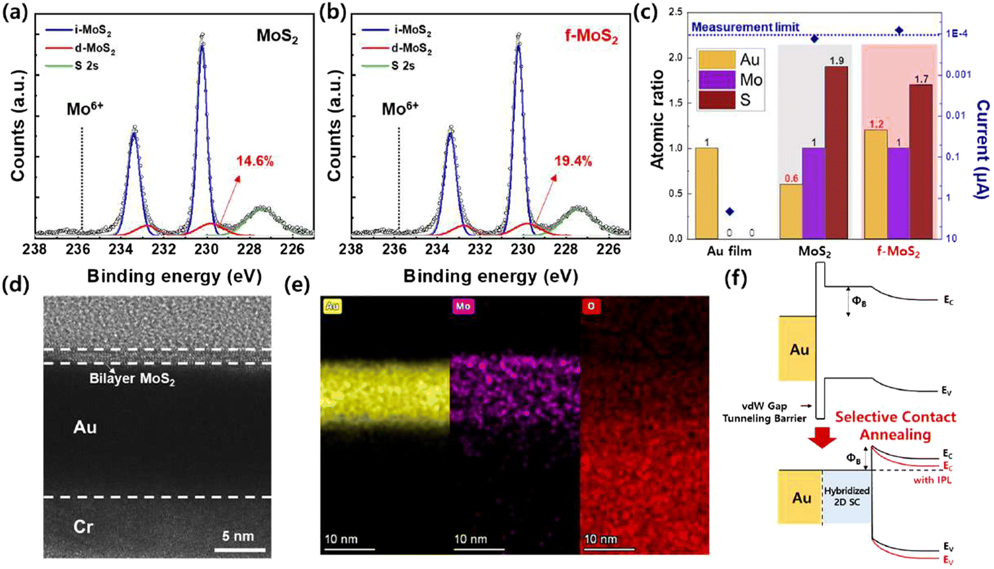 | ||
| Fig. 3 High-resolution XPS patterns of Mo 3d of (a) MoS2 and (b) f-MoS2. (c) Histogram of the relative atomic ratio (black) of each element (Au, Mo, and S) and the average current (blue) measured using C-AFM. The atomic ratio was normalized by the amount of Mo before and after the flash lamp irradiation. (d) Cross-sectional TEM images of MoS2/Au/Cr. (e) EDS mapping to confirm the absence of oxidation of MoS2. (f) Schematic image of the corresponding band diagram before and after hybridization between MoS2 and Au in the flash annealing process. | ||
TEM analysis confirmed the presence of a uniform MoS2 bilayer on the Au surface, with no additional MoO3 layer observed. This finding aligns with the XPS results, confirming that no unwanted oxidation occurred during the IPL process. Furthermore, a new layer was identified at the interface between MoS2 and Au. EDS mapping analysis indicates that this layer is composed of Mo, S, and Au elements, indirectly suggesting the formation of a MoS2–Au hybridization layer (Fig. 3e). Fig. 3f illustrates the corresponding band diagram of the MoS2–Au interface before and after selective flash annealing on the conductive area. The rapid decrease in RC can be attributed to the generation of sulfur vacancies and the formation of a MoS2–Au hybridization layer. The tunneling barrier is effectively eliminated due to the van der Waals gap and the reduction in ΦB.
The improvement of the electrical characteristics by the IPL process can be verified in Fig. 4a. Comparative analysis conducted at the maximum overdrive voltage (VG − VT = 5 V) reveals an approximate 3.0-fold increase in the on-current for f-MoS2 in contrast to n-MoS2. Additionally, the field-effect mobility (μFE), extracted from the transconductance (gm) − VG curve at the voltage corresponding to the maximum transconductance, exhibits a notable improvement, approximately 4.0-fold higher, escalating from 3.4 to 13.4 cm2 V−1 s−1 (Fig. 4b). The negligible amount of Vth shift (delta Vth = 0.5 V) suggests that there is little increase in the carrier concentration in the channel, thereby suggesting that the improved electrical properties are primarily attributed to the mitigation of contact resistance.
 | ||
| Fig. 4 (a) Transfer curves of n-MoS2 and f-MoS2 with VD = 0.1 V. (b) Gm − VG curves of n-MoS2 and F-MoS2 with VD = 1 V (c) Plot of the Y-function with respect to VG and a fitted line to obtain the slope. (d) Comparison of the μ0 and μFE values of n-MoS2 and f-MoS2. Total, channel, and contact resistances as functions of the overdrive voltage of (e) n-MoS2 and (f) f-MoS2. | ||
The Y-function method has been applied in 2D FETs to extract their intrinsic mobility (μ0) under relatively low-bias conditions because it can exclude series resistance such as RC and channel interface resistance.11,40,41 Additionally, the effects of RC on device operation were verified by comparing μ0 and μFE.
Since the channel length of the devices fabricated in this study is classified as a long channel of 10 μm, the contact resistance was analyzed using the Y-function method, which not only allows accurate analysis at this channel length, but also allows the contact resistance to be extracted from the existing device without additional structural modifications. The Y-function can be calculated based on the transfer curve extracted from the MoS2 transistor at VD = 0.1 V and the Y function–VG curve is shown based on eqn (1) (Fig. 4c).
| Y = IDS/(gm)1/2 = (μ0Cox[W/L]VD)1/2(VG − VT) | (1) |
Accordingly, the Y-function curves of MoS2 FETs recorded at VD = 0.1 V using the gm values from Fig. 4b are presented in Figure Fig. 4c. To extract the μ0 values of MoS2 FETs upon flash treatment, each slope in the Y-function curves was extrapolated in Fig. 4c to obtain the values of 9.4 × 10⁻⁴ and 14.1 × 10⁻⁴ for the normal device (n-MoS2 FET) and the flash-annealed device (f-MoS2 FET), respectively. Fig. 4d shows the calculated μ0 and μFE values for n-MoS2 and f-MoS2, respectively. Similarly to μFE, the flash process led to a 2.2-fold improvement in the μ0 values from 9.3 to 20.6 cm2 V−1 s−1 for n-MoS2 and f-MoS2, respectively. As a result, it was verified that μFE accounted for 36% (n-MoS2) and 65% (f-MoS2) of μ0, respectively. This result indicates that selective annealing of the electrode through the flash process leads to an enhancement in the device performance by decreasing RC.
Next, the contact resistance was estimated on the gate overdrive voltage to support the above-mentioned explanation. For overlapping FET devices, the total resistance (Rtotal) is composed of two RCs for the drain and source contact areas and one channel resistance (Rch) caused by scattering effects. With regard to Rch, it decreases to a value close to 0 as the overdrive voltage (VG − VT) increases sufficiently, thus enabling the extraction of RC. Fig. 4e and f present Rtotal, Rch, and RC on VG − VT for n-MoS2 and f-MoS2, respectively, based on the following equations:
| Rtotal = 2RC + Rch | (2) |
| Rch ≈ 1/β(VG − VT), β = μ0CG/L2. | (3) |
As VG − VT increases, we observed that Rtotal and Rch gradually saturate due to the increase in the applied electron concentration. The finding suggests that RC reduced from 8.9 to 3.3 kΩ by 63% owing to the introduction of the flash process. This result indicates that selective annealing of the electrode through the flash process enables an enhancement in the device performance by decreasing RC. Moreover, other multiple devices on the same substrate exposed to the identical flash light also exhibited noticeable improvement in mobility, thus highlighting the overall effects for large-area treatment (Fig. S5c, ESI†).
It is well known that the Schottky contact, which appears at the interface between metals and 2D materials, such as MoS2 and WS2, can determine RC from the height of the Schottky barrier (ΦB). Accordingly, ΦB was evaluated for further verification of the effect of flash annealing on the contact properties using the Arrhenius method (Fig. 5a–f). The 2D thermionic emission equation used for the evaluation is defined as follows:
 | (4) |
 is the Richardson constant corrected for 2D materials, T is the absolute temperature, kB is the Boltzmann constant, and n is the ideal factor.42,43Fig. 5a and d show the transfer curves of n-MoS2 and f-MoS2, respectively. I–V measurement was performed by increasing the temperature from 158 to 338 K every 30 K, thus causing an increase in the thermionic emission current. Next, the Arrhenius plots were obtained for different gate biases from −0.4 to 2.0 V at VD = 1 V for n-MoS2 and f-MoS2 in Fig. 5b and e, respectively. Since each slope of the lines in the Arrhenius plots corresponds to ΦB, each ΦB can be plotted depending on the corresponding gate biases (Fig. 5c and f). Once VG exceeds the flat band voltage, the linearity of the ΦB−VG curve deviates from the original trend because of the soaring tunneling current. Therefore, ΦB values using Au as the contact metal were estimated to be 61 and 30 meV for n-MoS2 and f-MoS2, respectively. This finding supportively proves that selective annealing of the contact areas through flash irradiation can reduce RC by decreasing ΦB. 2D semiconductor-based transistors are considered suitable channel materials for the top layer of a 3D stacked structure for logic circuit implementation. In that sense, without causing unnecessary thermal damage to the underlying layers, the IPL process can selectively improve the contact resistance of contact areas. We hope that this selective and local flash-annealing can be utilized as an attractive next-generation process for 2D semiconductor devices in 3D stacked structures.
 | ||
| Fig. 5 Temperature-dependent ID − VG transfer curves of (a) the n-MoS2 FET and (d) the f-MoS2 FET from 158 to 338 K. Arrhenius plots of (b) the n-MoS2 FET at gate voltages from −1.4 to 1.0 V and (e) the f-MoS2 FET at VG from −0.4 to 2.0 V. Extracted effective barrier heights (ΦSB) of (c) the n-MoS2 FET and (f) the f-MoS2 FET as a function of VGS. | ||
Conclusions
In this study, we proposed a novel and facile approach for improving the contact characteristics between 2D material channels and metal electrodes through ultrafast flash annealing by selectively heating the defined conducting areas in ambient air. We performed thermal simulation using COMSOL Multiphysics to verify that the entire temperature of the Au area on the MoS2 FETs was photo-thermally annealed over 640 K under light with a total energy density of 19.9 J cm−2. It was observed in the transfer curve that the mobility of flash-annealed MoS2 FETs increased along with the on-current. With respect to the output curve, the switching characteristics in the linear region were distinctly enhanced, thus indicating a decrease in the contact resistance between MoS2 and Au. For a better understanding, we applied the Y-function method to extract μ0, which was then compared to μFE. The results indicated a 2.2-fold increase in μ0 and a 4.0-fold increase in μFE at the flash light. It was further found that RC reduced by 63% from 8.9 to 3.3 kΩ by the introduction of a flash process with ΦB decreasing from 61 to 30 meV. Based on the results of optical measurements such as Raman and PL analyses, we reasoned that the striking improvement in contact characteristics can possibly result from the hybridization between Au and MoS2 during flash exposure and the increase in electron concentration due to the creation of sulfur vacancies. These aspects not only demonstrate that our IPL process with a low heat budget is an effective method for reducing contact resistance in two-dimensional materials, but also suggest new possibilities for the three-dimensional integration of two-dimensional materials.Method
MoS2 growth
The MoS2 thin film was synthesized in an inner quartz tube (2 in.) located in an outer quartz-tube (4 in.) furnace. High-purity Ar gas was used as a carrier gas that flowed along the 4 in. quartz tube at a pressure of 750 Torr (ESI S1†). As shown in Fig. S1a, ESI,† 120 mg of sulfur powder was prepared at the upstream of the furnace (heater 1). For Mo sources, 3.0–3.5 mg of molybdenum trioxide (MoO3) powder was placed at the downstream of the furnace (heater 2) with the Si/SiO2 growth substrate faced down. Note that perylene-3,4,9,10-tetracarboxylic acid tetrapotassium salt (PTAS) was added to the growth substrate as a seeding promoter. Afterwards, heater 1 and heater 2 were heated up to a temperature of 830 and 320 °C, respectively, during the main step of MoS2 growth as shown in Fig. S1b, ESI.†Device fabrication and electrical property characterization
The Si/SiO2 substrate was cleaned using piranha solution (H2SO4![[thin space (1/6-em)]](https://www.rsc.org/images/entities/char_2009.gif) :H2O2 = 1:1) for 10 min at room temperature, followed by deionized water (DI) rinsing. Afterwards, source and drain patterning was defined by the introduction of negative PR and subsequent photolithography. Then, Cr (5 nm)/Au (50 nm) was thermally deposited at ≈10−6 Torr by thermal evaporation. Next, MoS2 synthesized by chemical vapor deposition was transferred on the source and drain formed on the prepared substrate by the PS-assisted method, which was reported elsewhere.44 Intense pulsed light (IPL) with a xenon flash lamp (PLT, Photocura) was introduced to perform selective and ambient-air flash annealing on the source and drain area. After the flash annealing, the MoS2 channel region was defined on positive PR (GXR-601) with O2 plasma exposure, followed by deposition of 25 nm Al2O3 as the gate and blocking oxide by atomic layer deposition. Lastly, the gate electrode in the form of Cr (5 nm)/Au (50 nm) was patterned on the fabricated substrate by photolithography on an NR 9 resist. Finally, post-annealing was performed at 150 °C for 90 min at a ramping rate of 2 °C min−1. We used a parameter analyzer (Keithley, 4200 SCS) and a probe station (MS-TECH, MST-1000B) for characterization of the electrical properties from each fabricated device. Note that all measurements were performed under dark and vacuum conditions (∼50 mTorr).
:H2O2 = 1:1) for 10 min at room temperature, followed by deionized water (DI) rinsing. Afterwards, source and drain patterning was defined by the introduction of negative PR and subsequent photolithography. Then, Cr (5 nm)/Au (50 nm) was thermally deposited at ≈10−6 Torr by thermal evaporation. Next, MoS2 synthesized by chemical vapor deposition was transferred on the source and drain formed on the prepared substrate by the PS-assisted method, which was reported elsewhere.44 Intense pulsed light (IPL) with a xenon flash lamp (PLT, Photocura) was introduced to perform selective and ambient-air flash annealing on the source and drain area. After the flash annealing, the MoS2 channel region was defined on positive PR (GXR-601) with O2 plasma exposure, followed by deposition of 25 nm Al2O3 as the gate and blocking oxide by atomic layer deposition. Lastly, the gate electrode in the form of Cr (5 nm)/Au (50 nm) was patterned on the fabricated substrate by photolithography on an NR 9 resist. Finally, post-annealing was performed at 150 °C for 90 min at a ramping rate of 2 °C min−1. We used a parameter analyzer (Keithley, 4200 SCS) and a probe station (MS-TECH, MST-1000B) for characterization of the electrical properties from each fabricated device. Note that all measurements were performed under dark and vacuum conditions (∼50 mTorr).
Flash annealing by IPL treatment
A xenon flash lamp (PLT, Photocura) was utilized as a light source to perform selective and ambient-air flash annealing on the source and drain area. The IPL process features the spectrum range of 300–1000 nm. Spectrum information of the flash light with an energy density of ∼3.0 J cm−2 was examined using a compact spectrometer (Thorlabs, CCS200). The optical energy density was adjusted by tailoring the applied voltage, the pulse on time, the repetition rate of flashlight irradiation, the output pulse shape, and the distance between the lamp and the fabricated devices. In this study, various light energies from 15.6 to 24.3 J cm−2 (15.6, 19.9, 21.2, and 24.3 J cm−2) were applied to confirm the optimized device conditions. It was found that the device irradiated with a light energy density of 19.9 J cm−2 exhibits the best performance when it comes to FET device properties (ESI S11†).Numerical simulation for light–materials interactions
Based on the measured data, the total energy applied during the photothermal treatment was determined to be 19.9 J cm−2. The light absorption rates for each material were measured using the values reported from the relevant literature, enabling the calculation of the actual energy for heat generation inside the materials after photon–electron coupling. Considering the absorbable wavelength, absorbance was set as 0.2,20 0.6,45 and 0.1511 for MoS2, Au, and SiO2, respectively. Besides, time-dependent variables must be taken into account since the light-absorbed energy is not instantaneously converted entirely into thermal energy but is gradually transformed into heat for a certain period. Assuming that the light absorption by the material and the resulting photothermal reaction occur uniformly during an exposure time of 20 ms, a mathematical equation of a single square waveform was introduced to enable the total absorbed energy. Afterwards, the total energy actually absorbed by the material is converted into heat via the photothermal effect. Heat transfer analyses were conducted using COMSOL Multiphysics. For the heat transfer simulation, the temperatures of MoS2, Au, and SiO2 under flash light irradiation were determined using the following heat flux equation, eqn (5):46,47 | (5) |
Author contributions
Jun-Hwe Cha: conceptualization, investigation, visualization, writing – original draft and writing – review & editing. Inseong Lee: formal analysis, visualization, data curation and writing – review & editing. Seol Won Yun: investigation, methodology and software. Woonggi Hong, Hyo Hoon Byeon, Jungyeop Oh and Seohak Park: writing – review & editing. Sung-Yool Choi: funding acquisition, resources, project administration, supervision and writing – review & editing. All authors participated in general discussion and manuscript revision.Data availability
All relevant data are available from the authors on reasonable request and/or are included within the article and the ESI.†Conflicts of interest
There are no conflicts to declare.Acknowledgements
This work was supported by the National Research Foundation of Korea (NRF) grant funded by the Korea government (MSIT) (RS-2025-00514270); the Semiconductor-Secondary Battery Interfacing Platform Technology Development Project of NNFC (2710018562); Samsung Electronics (IO221219-04252-01); and the Korea Institute for Advancement of Technology (KIAT) grant funded by the Korea Government (MOTIE) (RS-2023-KI002692, HRD Program for Industrial Innovation).References
- M. Koyanagi, Recent progress in 3D integration technology, IEICE Electron. Express, 2015, 12(7), 20152001–20152001 CrossRef.
- C. G. Hwang , New paradigms in the silicon industry, 2006 International Electron Devices Meeting 2006, vol. 1 and 2, pp. 274–281.
- Y. Shen, Z. Y. Dong, Y. B. Sun, H. Guo, F. Wu, X. L. Li, J. Tang, J. Liu, X. Wu, H. Tian and T. L. Ren, The Trend of 2D Transistors toward Integrated Circuits: Scaling Down and New Mechanisms, Adv. Mater., 2022, 34(48), 2201916 CrossRef CAS.
- L. R. Thoutam, R. Mathew, J. Ajayan, S. Tayal and S. V. Nair, A critical review of fabrication challenges and reliability issues in top/bottom gated MoS2 field-effect transistors, Nanotechnology, 2023, 34(23), 232001 CrossRef CAS.
- R. Mathew and J. Ajayan, Material processing, performance and reliability of MoS2 field effect transistor (FET) technology-A critical review, Mater. Sci. Semicond. Process., 2023, 160, 107397 CrossRef CAS.
- S. Das, H. Y. Chen, A. V. Penumatcha and J. Appenzeller, High Performance Multilayer MoS2 Transistors with Scandium Contacts, Nano Lett., 2013, 13(1), 100–105 CrossRef CAS PubMed.
- G. W. Shim, W. Hong, J. H. Cha, J. H. Park, K. J. Lee and S. Y. Choi, TFT Channel Materials for Display Applications: From Amorphous Silicon to Transition Metal Dichalcogenides, Adv. Mater., 2020, 32(35), 1907166 CrossRef CAS PubMed.
- H. Liu, A. T. Neal and P. D. D. Ye, Channel Length Scaling of MoS2 MOSFETs, ACS Nano, 2012, 6(10), 8563–8569 CrossRef CAS.
- T. Knobloch, S. Selberherr and T. Grasser, Challenges for Nanoscale CMOS Logic Based on Two-Dimensional Materials, Nanomaterials, 2022, 12(20), 3548 CrossRef CAS.
- D. S. Schulman, A. J. Arnold and S. Das, Contact engineering for 2D materials and devices, Chem. Soc. Rev., 2018, 47(9), 3037–3058 RSC.
- J. K. Han, J. Y. Park, C. K. Kim, J. H. Kwon, M. S. Kim, B. W. Hwang, D. J. Kim, K. C. Choi and Y. K. Choi, Electrothermal Annealing to Enhance the Electrical Performance of an Exfoliated MoS2 Field-Effect Transistor, IEEE Electron Device Lett., 2018, 39(10), 1532–1535 CAS.
- S. Zhang, R. Li, Z. Yao, P. Liao, Y. Li, H. Tian, J. Wang, P. Liu, J. Guo, K. Liu, F. Mei and L. Liu, Laser annealing towards high-performance monolayer MoS2 and WSe2 field effect transistors, Nanotechnology, 2020, 31(30), 30LT02 CrossRef CAS PubMed.
- S. Cho, S. Kim, J. H. Kim, J. Zhao, J. Seok, D. H. Keum, J. Baik, D. H. Choe, K. J. Chang, K. Suenaga, S. W. Kim, Y. H. Lee and H. Yang, Phase patterning for ohmic homojunction contact in MoTe2, Science, 2015, 349(6248), 625–628 CrossRef CAS PubMed.
- R. Kappera, D. Voiry, S. E. Yalcin, W. Jen, M. Acerce, S. Torrel, B. Branch, S. D. Lei, W. B. Chen, S. Najmaei, J. Lou, P. M. Ajayan, G. Gupta, A. D. Mohite and M. Chhowalla, Metallic 1 T phase source/drain electrodes for field effect transistors from chemical vapor deposited MoS2, APL Mater., 2014, 2(9), 092516 CrossRef.
- A. Pelella, O. Kharsah, A. Grillo, F. Urban, M. Passacantando, F. Giubileo, L. Iemmo, S. Sleziona, E. Pollmann, L. Madauss, M. Schleberger and A. Di Bartolomeo, Electron Irradiation of Metal Contacts in Monolayer MoS2 Field-Effect Transistors, ACS Appl. Mater. Interfaces, 2020, 12(36), 40532–40540 CrossRef CAS.
- W. Liu, D. Sarkar, J. H. Kang, W. Cao and K. Banerjee, Impact of Contact on the Operation and Performance of Back-Gated Monolayer MoS2 Field-Effect-Transistors, ACS Nano, 2015, 9(8), 7904–7912 CrossRef CAS.
- B. T. Blue, G. G. Jernigan, D. Le, J. J. Fonseca, S. D. Lough, J. E. Thompson, D. D. Smalley, T. S. Rahman, J. T. Robinson and M. Ishigami, Metallicity of 2H-MoS2 induced by Au hybridization, 2D Mater., 2020, 7(2), 025021 CrossRef CAS.
- A. Islam, J. Lee and P. X. L. Feng, All-dry transferred single- and few-layer MoS2 field effect transistor with enhanced performance by thermal annealing, J. Appl. Phys., 2018, 123(2), 025701 CrossRef.
- H. J. Kwon, S. Kim, J. Jang and C. P. Grigoropoulos, Evaluation of pulsed laser annealing for flexible multilayer MoS2 transistors, Appl. Phys. Lett., 2015, 106(11), 113111 CrossRef.
- H. Kwon, W. Choi, D. Lee, Y. Lee, J. Kwon, B. Yoo, C. P. Grigoropoulos and S. Kim, Selective and localized laser annealing effect for high-performance flexible multilayer MoS2 thin-film transistors, Nano Res., 2014, 7(8), 1137–1145 CrossRef CAS.
- T. H. Im, J. H. Lee, H. S. Wang, S. H. Sung, Y. B. Kim, Y. Rho, C. P. Grigoropoulos, J. H. Park and K. J. Lee, Flashlight-material interaction for wearable and flexible electronics, Mater. Today, 2021, 51, 525–551 CrossRef CAS.
- J. H. Cha, D. H. Kim, C. Park, S. J. Choi, J. S. Jang, S. Y. Yang, I. Kim and S. Y. Choi, Low-Thermal-Budget Doping of 2D Materials in Ambient Air Exemplified by Synthesis of Boron-Doped Reduced Graphene Oxide, Adv. Sci., 2020, 7(7), 1903318 CrossRef CAS.
- D.-H. Kim, J.-H. Cha, G. Shim, Y. H. Kim, J.-S. Jang, H. Shin, J. Ahn, S.-Y. Choi and I.-D. Kim, Flash-thermochemical engineering of phase and surface activity on metal oxides, Chem, 2022, 8(4), 1014–1033 CAS.
- J. M. Shin, J. H. Choi, D. H. Kim, H. K. Jang, J. Yun, J. Na and G. T. Kim, Induction heating effect on the performance of flexible MoS2 field-effect transistors, Appl. Phys. Lett., 2017, 111(15), 153105 CrossRef.
- H. Kwon, S. Baik, J. E. Jang, J. Jang, S. Kim, C. P. Grigoropoulos and H. J. Kwon, Ultra-Short Pulsed Laser Annealing Effects on MoS2 Transistors with Asymmetric and Symmetric Contacts, Electronics, 2019, 8(2), 222 CrossRef CAS.
- M. F. Abdel Messih, A. E. Shalan, M. F. Sanad and M. A. Ahmed, RETRACTED ARTICLE: Facile approach to prepare ZnO@ SiO2 nanomaterials for photocatalytic degradation of some organic pollutant models, J. Mater. Sci.:Mater. Electron., 2019, 30(15), 14291–14299 CrossRef CAS.
- A. Castellanos-Gomez, J. Quereda, H. P. van der Meulen, N. Agraït and G. Rubio-Bollinger, Spatially resolved optical absorption spectroscopy of single-and few-layer MoS2 by hyperspectral imaging, Nanotechnology, 2016, 27(11), 115705 CrossRef PubMed.
- K. F. Mak, K. He, C. Lee, G. H. Lee, J. Hone, T. F. Heinz and J. Shan, Tightly bound trions in monolayer MoS2, Nat. Mater., 2013, 12(3), 207–211 CrossRef CAS.
- K. Chen, A. Roy, A. Rai, A. Valsaraj, X. Meng, F. He, X. Xu, L. F. Register, S. Banerjee and Y. Wang, Carrier trapping by oxygen impurities in molybdenum diselenide, ACS Appl. Mater. Interfaces, 2018, 10(1), 1125–1131 CrossRef CAS PubMed.
- K. Golasa, M. Grzeszczyk, M. R. Molas, M. Zinkiewicz, L. Bala, K. Nogajewski, M. Potemski, A. Wysmolek and A. Babinski, Resonant quenching of Raman scattering due to out-of-plane A1g/A‘1 modes in few-layer MoTe2, Nanophotonics, 2017, 6(6), 1281–1288 CrossRef CAS.
- F. Bozheyev, R. Nemkayeva, N. Guseinov, M. Kaikanov and A. Tikhonov, Photoluminescence quenching of WS2 nanoflakes upon Ga ion irradiation, J. Lumin., 2020, 217, 116786 CrossRef CAS.
- M. Buscema, G. A. Steele, H. S. J. van der Zant and A. Castellanos-Gomez, The effect of the substrate on the Raman and photoluminescence emission of single-layer MoS2, Nano Res., 2014, 7(4), 561–571 CrossRef.
- H. Park, G. H. Shin, K. J. Lee and S. Y. Choi, Probing temperature-dependent interlayer coupling in a MoS2/h-BN heterostructure, Nano Res., 2020, 13(2), 576–582 CrossRef CAS.
- I. Lee, M. Kang, S. Park, C. Park, H. Lee, S. Bae, H. Lim, S. Kim, W. Hong and S. Y. Choi, Healing Donor Defect States in CVD–Grown MoS2 Field–Effect Transistors Using Oxygen Plasma with a Channel–Protecting Barrier, Small, 2024, 20(2), 2305143 CrossRef CAS PubMed.
- S. Tongay, J. Suh, C. Ataca, W. Fan, A. Luce, J. S. Kang, J. Liu, C. Ko, R. Raghunathanan, J. Zhou, F. Ogletree, J. Li, J. C. Grossman and J. Wu, Defects activated photoluminescence in two-dimensional semiconductors: interplay between bound, charged and free excitons, Sci. Rep., 2013, 3(1), 2657 CrossRef PubMed.
- T. Verhagen, V. L. Guerra, G. Haider, M. Kalbac and J. Vejpravova, Towards the evaluation of defects in MoS2 using cryogenic photoluminescence spectroscopy, Nanoscale, 2020, 12(5), 3019–3028 RSC.
- S. Y. Cho, H. J. Koh, H. W. Yoo, J. S. Kim and H. T. Jung, Tunable Volatile-Organic-Compound Sensor by Using Au Nanoparticle Incorporation on MoS2, ACS Sens., 2017, 2(1), 183–189 CrossRef CAS PubMed.
- H. Yin, D. F. Hu, X. M. Geng, H. Liu, Y. F. Wan, Z. H. Guo and P. Yang, 2D gold supercrystal-MoS2 hybrids: Photoluminescence quenching, Mater. Lett., 2019, 255, 126531 CrossRef CAS.
- U. Bhanu, M. R. Islam, L. Tetard and S. I. Khondaker, Photoluminescence quenching in gold - MoS2 hybrid nanoflakes, Sci. Rep., 2014, 4(1), 5575 CrossRef CAS PubMed.
- H. Y. Chang, W. N. Zhu and D. Akinwande, On the mobility and contact resistance evaluation for transistors based on MoS2 or two-dimensional semiconducting atomic crystals, Appl. Phys. Lett., 2014, 104(11), 113504 CrossRef.
- F. Urban, G. Lupina, A. Grillo, N. Martucciello and A. Di Bartolomeo, Contact resistance and mobility in back-gate graphene transistors, Nano Express, 2020, 1(1), 010001 CrossRef CAS.
- A. Allain, J. H. Kang, K. Banerjee and A. Kis, Electrical contacts to two-dimensional semiconductors, Nat. Mater., 2015, 14(12), 1195–1205 CrossRef CAS PubMed.
- E. Yarali, C. Koutsiaki, H. Faber, K. Tetzner, E. Yengel, P. Patsalas, N. Kalfagiannis, D. C. Koutsogeorgis and T. D. Anthopoulos, Recent Progress in Photonic Processing of Metal-Oxide Transistors, Adv. Funct. Mater., 2020, 30(20), 1906022 CrossRef CAS.
- W. Hong, G. W. Shim, S. Y. Yang, D. Y. Jung and S. Y. Choi, Improved Electrical Contact Properties of MoS2-Graphene Lateral Heterostructure, Adv. Funct. Mater., 2019, 29(6), 1807550 CrossRef.
- J. Wang, Q. Ran, X. Xu, B. Zhu and W. Zhang, in Preparation and Optical Properties of TiO2-SiO2thin films by Sol-gel Dipping Method, IOP Conference Series: Earth and Environmental Science, IOP Publishing, 2019, p. 042029.
- Z. Wang, J. E. Alaniz, W. Jang, J. E. Garay and C. Dames, Thermal conductivity of nanocrystalline silicon: importance of grain size and frequency-dependent mean free paths, Nano Lett., 2011, 11(6), 2206–2213 CrossRef CAS PubMed.
- D. H. Jung, J. H. Park, H. E. Lee, J. Byun, T. H. Im, G. Y. Lee, J. Y. Seok, T. Yun, K. J. Lee and S. O. Kim, Flash-induced ultrafast recrystallization of perovskite for flexible light-emitting diodes, Nano Energy, 2019, 61, 236–244 CrossRef CAS.
- K. F. Mak, C. Lee, J. Hone, J. Shan and T. F. Heinz, Atomically Thin MoS2: A New Direct-Gap Semiconductor, Phys. Rev. Lett., 2010, 105(13), 136805 CrossRef PubMed.
Footnotes |
| † Electronic supplementary information (ESI) available. See DOI: https://doi.org/10.1039/d5nr00114e |
| ‡ These authors contributed equally to this work. |
| This journal is © The Royal Society of Chemistry 2025 |