
 Open Access Article
 This Open Access Article is licensed under a Creative Commons Attribution-Non Commercial 3.0 Unported Licence
Synthesis and sintering of AgNWs@PVP core–shell structures for improved transparent electrodes
Tang Xianjie a,
Gan Guoyou*a,
Chen Shouzhia,
Yu Xiangleia,
Qian Zhuoa and
Li Junpengb
a,
Gan Guoyou*a,
Chen Shouzhia,
Yu Xiangleia,
Qian Zhuoa and
Li Junpengb
aFaculty of Materials Science and Engineering, Kunming University of Science and Technology, Kunming 650093, Yunnan, China. E-mail: ganguoyou@kust.edu.cn
bSino-Platinum Metals Co Ltd, Kunming 650106, Yunnan, China
First published on 25th February 2025
Abstract
The majority of the current composite core–shell structure preparation and sintering processes applied to silver nanowire transparent electrodes are impractical for large-scale industrial production and primarily emphasize macroscopic performance parameters, with limited insights into the underlying sintering mechanism. This study presents a simple synthesis of AgNWs@PVP core–shell structures and investigates the effects of sintering temperature and time on their morphology. The morphology of AgNWs@PVP core–shell structures during sintering was systematically analyzed using characterization techniques, such as transmission electron microscopy and scanning electron microscopy. Subsequently, a comprehensive understanding of its sintering mechanism was summarized. This provides theoretical foundation for the preparation of AgNWs-based core–shell structures and high-temperature sintering based on core–shell structures.
1. Introduction
Due to quantum size effect, surface effect, and quantum tunnelling effect, when the particle scale reaches the nanoscale it leads to drastic changes in the physical and chemical properties of the particle. Various metallic nanoparticles have been produced with different biochemical and physicochemical properties, which make it possible to apply novel technologies to devices.1–3 And metal nanowire-like structures have a wide range of properties that cannot be achieved with nanospheres.4 In recent years, silver nanowires (AgNWs) have attracted significant attention due to their excellent electrical and thermal conductivity.5 The utilization of AgNWs as an alternative to indium tin oxide materials has emerged as one of the breakthroughs in the field of transparent conducting electrode research.6,7 AgNWs-based transparent conducting electrodes have been applied in optoelectronic devices, organic solar cells, sensors, and electromagnetic shielding film.8–17 The polyol method is widely used in the preparation of AgNWs, with polyvinylpyrrolidone (PVP) playing a key role in promoting their linear growth. However, excess PVP increases contact resistance, necessitating preferentially removal of PVP to ensure their excellent conductivity.18 After removing the PVP, the pure AgNWs need to be prepared as core–shell structures using techniques such as sputtering and atomic layer deposition, or as multilayer composite structures using spin-coating and spraying.19–21 These structures are then subjected to post-treatment processes such as high-temperature hot pressing and microwave sintering to reduce contact resistance and improve stability.22,23 However, most of the reported methods for preparing core–shell structures of AgNWs are complex, costly, and unsuitable for industrial production. Furthermore, most studies focus on enhancing macroscopic performance parameters while providing limited theoretical insights into the sintering mechanism. To address these challenges, this study developed AgNWs@PVP core–shell structures using a simplified method. By controlling the thickness of PVP layer, the structures retained the thermal stability provided by PVP while overcoming its insulating limitations through the application of tunneling current theory. Moreover, a simple high-temperature sintering post-treatment was carried out to investigate the effects of sintering temperature and time on the AgNWs@PVP core–shell structure and the sintering mechanism was further analyzed.2. Method
2.1 Chemicals
All chemicals were used without further purification. Ethanol (>99%), isopropanol (>99%), tetrabutylammonium chloride (>99%), polyvinylpyrrolidone (PVP, molecular weight: 58![[thin space (1/6-em)]](https://www.rsc.org/images/entities/char_2009.gif) 000), and ethylene glycol (anhydrous, 99.8%) were purchased from Aladdin. AgNO3 (>99%) was purchased from Sino-Platinum Metals Co Ltd.
000), and ethylene glycol (anhydrous, 99.8%) were purchased from Aladdin. AgNO3 (>99%) was purchased from Sino-Platinum Metals Co Ltd.
2.2 Preparation of AgNWs
In a typical synthetic procedure, 0.34 g PVP (molecular weight: 58000) was dissolved into 20 mL ethylene glycol in a 25 mL three-necked round bottom flask. The mixture was heated to 160 °C and stirred at 800 rpm. After 10 min, 0.02 g tetrabutylammonium chloride was added. Following an additional 5 min, AgNO3 was added dropwise at a rate of 0.8 mL min−1. Subsequently, the reaction solution was cooled to room temperature, transferred into a centrifuge tube, and diluted with ethanol. After thorough dispersion, it was centrifuged at 5000 rpm for 5 min at a time using a bench-top high-speed centrifuge.
2.3 Preparation of AgNWs@PVP core shells
First, PVP (molecular weight: 58000) was dissolved in ethanol (10 mL). Then, AgNW solution (10 mL) was added, and the mixture was stirred vigorously for 90 min. Subsequently, the resulting suspension was centrifuged at 4000 rpm for 5 min to obtain a grey-black solid. Finally, the solid was re-dispersed in 10 mL of ethanol. Different amounts of PVP (0.04, 0.06, and 0.08 g) were used to adjust the thickness of the PVP shell layer.
2.4 Preparation of silver nanowire transparent conducting electrodes
0.6 mL of AgNW dispersion (2.5 mg mL−1) was spin-coated onto the surface of clean 5 cm × 5 cm glass slides at 1000 rpm for 40 s. The coated slides were then dried in an oven at different temperatures for different durations.2.5 Characterization
A high-resolution scanning electron microscope (SEM, Hitachi SU8010) was used to examine the microscopic morphology of specimens. Transmission electron microscopy (TEM, FEI Talos F200×, Hillsboro, OR, USA) was employed to obtain higher magnification information. The elemental analysis was performed using X-ray photoelectron spectroscopy (XPS, Thermo Scientific K-Alpha, USA). The square resistance was characterised by a digital four-probe tester (ST-2258C, JG, China). The transmittance (T%) of the silver wire conductive films was measured using a UV-vis spectrophotometer (Metash, CHINA), where the glass substrate was used as a blank control.3. Result and discussion
Fig. 1a shows the overall morphology of AgNWs prepared by liquid phase synthesis after a single centrifugation. The AgNWs were coated with residual PVP, with relatively uniform dimensions: lengths of 10–20 μm and diameters of 30–50 nm, and few impurities such as silver nanoparticles. Fig. 1b shows the overall morphology of the AgNWs after 10 centrifugations, and the PVP in the outer layer of the AgNWs was almost completely removed. This was further supported by the XPS results in Fig. 1d, where the intensity of the C, O, and N peaks decreased dramatically. The weak remaining peaks may result from atmospheric contamination. The lattice stripe width of AgNWs can be seen in Fig. 1c as 0.242 nm, which corresponded to the {111} crystallographic family of silver. | ||
| Fig. 1 (a) SEM image of AgNWs before centrifugal cleaning. (b) SEM images of AgNWs after centrifugal cleaning. (c) TEM images of AgNWs used in this work. (d) XPS images of AgNWs before and after centrifugation and XPS images of PVP. | ||
The AgNWs@PVP core–shell structures were obtained by adding different amounts of PVP with vigorous stirring after obtaining pure silver nanowire samples. Fig. 2a–c show the TEM images of the shell layer thicknesses of AgNWs@PVP core–shell structures after adding 0.04 g, 0.06 g, and 0.08 g of PVP, respectively. It can be seen that the overall thickness of the shell layer was uniform after the addition of different amounts of PVP. The thickness ranges of the shell layer after addition of different amounts of PVP were 1.20 ± 0.03 nm, 2.11 ± 0.01 nm and 3.03 ± 0.01 nm, respectively. PVP was used as an organic cladding layer, and the thicker PVP layer enhanced the thermal stability and corrosion resistance of AgNWs. However, according to the theory of tunneling current, due to the poor conductivity of the PVP layer, increased thickness adversely affected conductivity, and an excessively thick PVP layer can render the tunneling current invalid. Fig. 2d presents the square resistance of AgNWs with PVP layers of 1.20 ± 0.03 nm, 2.11 ± 0.01 nm, and 3.03 ± 0.01 nm thicknesses after spin-coating without post-processing. The square resistance increased with the thickness of the PVP coating layer, with a pronounced rise observed at 3.03 ± 0.01 nm. This indicated that the higher thickness of PVP had a greater effect on the tunneling current, with the best conductivity at a thickness of 1.20 ± 0.03 nm, followed by 2.11 ± 0.01 nm, and approaching the limit of tunneling current failure at 3.03 ± 0.01 nm, 3.03 ± 0.01 nm.24
 | ||
| Fig. 2 TEM images of AgNWs@PVP shell layer structures prepared with different PVP contents: (a) 0.04 g, (b) 0.06 g, and (c) 0.08 g. (d) Variation sheet resistance of (a)–(c) films. | ||
In order to balance the effect of different thicknesses of PVP layers on the electrical conductivity and thermal stability, Fig. 3 illustrates the SEM images of AgNWs@PVP core–shell structures with different PVP thicknesses after sintering at 190 °C for 30 min. The inner area of the red circle in each figure was the area of the X-contact junction and the area where the morphology had changed. From Fig. 3a, it can be observed that the AgNWs@PVP core–shell structure with a PVP thickness of 1.20 ± 0.03 nm partially fractured at the X-junction. It indicated that the AgNWs@PVP core–shell structure was poorly thermally stabilised at this thickness and cannot form a complete welded network. The AgNWs@PVP core–shell structure with a PVP thickness of 2.11 ± 0.01 nm in Fig. 3b formed a fully welded junction at the X-junction, with no visible fractures. It indicated that the thermal stability provided by PVP at this thickness can support sintering at the AgNWs junction. The AgNWs@PVP core–shell structure with a PVP thickness of 3.03 ± 0.01 nm in Fig. 3c showed a transparent softening at the X-junction, and the boundaries between the overlapping AgNWs remain distinct, indicating incomplete sintering. The PVP partially softened to form a transparent layer at the junction. It indicated that the PVP at this thickness provides too much thermal stability for the AgNWs@PVP core–shell structure to be fully sintered. Fig. 3d shows the square resistance and transmittance data of AgNWs@PVP core–shell structures sintered at 190 °C for 30 min with different PVP thicknesses. The AgNWs@PVP core–shell structure with a PVP thickness of 2.11 ± 0.01 nm achieved the best overall performance, with an average relative transmittance of 92.5% and an average square resistance of 34.3 Ω sq−1. These results suggested that PVP layer thickness directly impacted the transmittance. Thinner layers (e.g., 1.20 ± 0.03 nm) had the best conductivity before sintering but lacked sufficient thermal stability to cause fracture during the sintering process. However, thicker layers (e.g., 3.03 ± 0.01 nm) reduced the transmittance and resulted in incomplete softening of the PVP due to excessive thermal stability, preventing junction soldering. After balancing the effects of tunneling current and AgNWs protection on the film, a thickness of 2.11 ± 0.01 nm was more suitable. This specific thickness ensured that the AgNWs@PVP film network had an optimal square resistance and protected the AgNWs while enabling effective junction welding during the high temperature annealing process.
 | ||
| Fig. 3 SEM images of AgNWs@PVP core–shell layer structures with different PVP thicknesses and statistical plots of sheet resistance and transmittance after high-temperature sintering. (a) 1.20 ± 0.03 nm, (b) 2.11 ± 0.01 nm, (c) 3.03 ± 0.01 nm, (d) statistical plots. | ||
As can be seen in Fig. 4, the typical contact mode during the soldering process of AgNWs was the X-type contact, while the head-to-head contact and the head-to-wire contact modes were not considered as major factors in this study. The inner area of the red circle in each figure was the area of the X-contact junction and the area where the morphology had changed. As shown in Fig. 4a, the AgNWs@PVP network with a width of ∼45 nm and a PVP cladding layer of ∼2.11 ± 0.01 nm showed almost no change at the junction after heating treatment at 150° for 30 min, which indicated that the PVP softening temperature as well as the sintering temperature of the AgNWs@PVP core–shell layer structure could not be reached at this temperature. From Fig. 4b, it can be observed that the PVP layer at the AgNWs joint appeared to be partially broadened after treatment at 170° for 30 min. Prolonging the heat treatment for another 30 min, irregular undulations appeared in the vicinity of the joint, where the upper AgNWs boundary was partially blurred, and a small portion of it was embedded in the lower AgNWs. This indicated that complete welding was not achieved even with extended welding times at this temperature. In Fig. 4d, after 30 min of treatment at 190°, the X-junctions were fully welded without any fractures. After 30 min of treatment at 210°, the junction at the lower right of Fig. 4e was partially fully welded, but the AgNWs joints in the middle were fractured due to thermal damage. However, fractures were only partial at this temperature, and no other phenomena were observed, prompting further increase in the heat treatment temperature. Fig. 4f shows the SEM images of the AgNWs@PVP network after heat treatment at 230° for 30 min. At this high temperature, the diameter of the AgNWs head region increased while the junction diameter decreased. This phenomenon occurs because, as the temperature rises, most of the welded joint has already formed. The original upper and lower AgNWs were in the same plane at this time, and the atoms tend to continue to flow along the axial direction, and the accelerated flow of atoms towards the head leads to an increase in the diameter of the head region, while the diameter of the joint decreases or even breaks.25
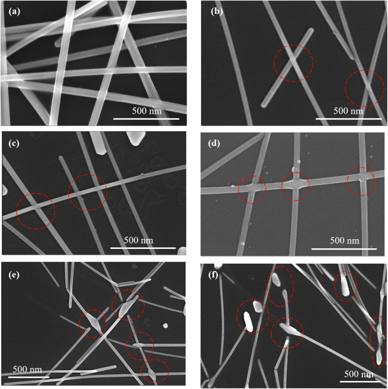 | ||
| Fig. 4 SEM images of AgNWs@PVP shell layer structures at different sintering temperature-durations. (a) 150 °C–30 min, (b) 170 °C–30 min, (c) 170 °C–60 min, (d) 190 °C–30 min, (e) 210 °C–30 min, (f) 230 °C–30 min. | ||
In order to further investigate the welding mechanism of the AgNWs@PVP core–shell structure network, SEM and TEM analyses were conducted at different time intervals during heat treatment at 190°. The inner area of the red circle in each figure was the area where the morphology had changed. Fig. 5a illustrates that after 10 min of heating, the X-junctions exhibited transparent-like broadening, and fine nanoparticles were uniformly distributed along the wires. Fig. 5c and d shows that silver nanoparticles of ∼5 nm appeared on the surface of the AgNWs. Fig. 5e and f shows that the spacing of lattice stripes of these silver nanoparticles in different directions is 0.237 nm and 0.241 nm, corresponding to the (111) crystal plane family. The mechanism of nanoparticle formation may be that at the interfaces of nanowires, accompanied by the thermal motion of the atoms under the capillary, locally raised nanostructures are induced, and silver atoms in these structures will be reoriented driven by surface energy, and interdiffusion between neighbouring nanostructures gradually results in the formation of single-crystal nanoparticles.25 And it can be seen from the figure that the overall diameter of AgNWs did not change significantly during the pre-sintering period, indicating that at this time the atoms on the nanowires were more inclined to escape from the surface rather than axial flow. However, the wires were not welded with each other at this time, which can be evidenced by the distinct surface structures of the AgNWs and the clearly visible superposition of intersecting wires. After 20 min of heat treatment at 190 °C, as shown in Fig. 5b, the number of fine nanoparticles gradually increased, while the boundary between the AgNWs at the junctions became less distinct. It was more difficult to distinguish the boundary between the wires and the wires. The possible reason for this phenomenon was that with the thermal movement under the capillary, the fine nanoparticles were driven by the surface energy to re-select the arrangement. When these nanoparticles aligned with AgNWs, they were reabsorbed and reorganized. As shown in Fig. 5b, nanoparticles located away from the junction gradually grow larger, while those at the interface migrated to fill the gaps between the wires, forming welded joints.
 | ||
| Fig. 5 SEM and TEM images of different welding durations at 190 °C welding temperature. (a) 10 min, (b) 20 min, (c) and (d) 10 min-TEM, (e) and (f) lattice fringes in region 1. | ||
Fig. 6 shows SEM images of AgNWs@PVP core–shell structure with different sintering times and of AgNWs@PVP core–shell structure with a certain curvature when sintered for 20 min. The inner regions of the red circles in each figure were the regions at the X-contact junctions as well as the regions where the morphology had changed. Fig. 6a presents the SEM image of the AgNWs@PVP core–shell structural network of high-temperature treatment at 190 °C for 30 min. The network became smoother, with the fine nanoparticles on the line continuing to increase in size but decrease in number. The X-junctions formed a more complete welded joint. The possible reason for this was that prolonged heat treatment allowed nanoparticles to be reabsorbed and rearranged, resulting in fewer fine nanoparticles, smoother silver surfaces, and progressive filling of voids at the junctions, achieving the most stable joints. In order to further investigate the effect of thermal excitation on the AgNWs@PVP network, the heat treatment time was further extended. Fig. 6b shows the SEM image of the AgNWs@PVP network treated at 190 °C for 50 min. The diameters of the AgNWs gradually showed an increasing trend, while the joints of the AgNWs@PVP joints appeared to be fractured. When the high-temperature treatment was extended, the silver particles at the joint complete the soldering process. Atomic flow favours axial movement, and the flow of atoms to the ends leads to an increase in the diameter of the silver filaments at both ends, while the connecting layer becomes thinner and the local stresses increase, thus increasing the risk of fracture. This was also evidenced by the SEM image of the AgNWs@PVP network treated at 190 °C for 100 min in Fig. 6c, where the atoms tended to continue to flow in the axial direction as the high-temperature treatment time was extended to 100 min, resulting in more fracture of the AgNWs at the joints under thermal perturbation. In addition, a phenomenon was found when heating at 190 °C for 20 min, as shown in Fig. 6d: the silver wires with lower curvature remained unsintered, while the AgNWs with higher curvature exhibited bending. This behavior can be attributed to the high-temperature treatment of silver wires induced residual stress, leading to a concentration of stress on silver wires with a certain curvature. Simulation results show that the maximum strain on the upper nanowire is about 0.5%, below which it is still in the elastic phase,25 but when the strain at the curvature location exceeds the elastic strain limit, these residual stresses cause strain and plastic deformation despite the surface being covered with a layer of nanoscale PVP. Consequently, AgNWs with a certain curvature exhibit lower thermal stability.
 | ||
| Fig. 6 SEM images of different welding durations at 190 °C welding temperature. (a) 30 min, (b) 50 min, (c) 100 min, (d) AgNWs with some curvature-20 min. | ||
The welding mechanism of the core–shell structure of AgNWs was elucidated through SEM and HRTEM analyses. During initial high-temperature treatment, the nanoscale PVP layer on the upper and lower AgNWs at the joints of the X-contacts was softened to different degrees due to the thermal perturbation brought by the high-temperature environment. As the sintering process continues, silver nanoparticles on the AgNWs bonded to the PVP escape from the PVP surface into the gap between the wires due to capillary-induced surface diffusion and infiltration. Then, the small nanoparticles gradually filled the gap and were re-selected to be rearranged under the drive of the surface energy. They were reabsorbed to form the soldered junction when these nanoparticles were aligned with the AgNWs. As the reaction time prolonged, most of the welded junctions were generated at the interface between the upper and lower layers of silver wires, and the atomic flow between the networks was more inclined to axial movement. However, extended exposure to high temperatures induced axial atomic flow, leading to increased wire diameters at the head regions and thinning of the connecting layers at the junctions, and an increase in localised stresses, which ultimately leads to network fracture.
4. Conclusion
Compared to methods that require complex and expensive experimental setups, such as ion sputtering for AgNWs core–shell structures, a simple method was proposed to prepare AgNWs@PVP core–shell composites. High-temperature sintering post-processing was conducted to explore the effects of the sintering temperature and duration on the AgNWs@PVP core–shell structure. The sintering mechanism was discussed and the main results are as follows:(1) The AgNWs@PVP core–shell structure with controllable thickness of the cladding layer can be obtained by adjusting the content of PVP. When the PVP cladding thickness is 2.11 ± 0.01 nm, the unsintered AgNWs@PVP film network exhibited moderate square resistance according to the tunnel current theory. And the AgNWs were effectively protected during the high-temperature annealing process and completed the junction welding.
(2) SEM images revealed that a complete weld at X-contact joints was achieved after sintering at 190 °C for 30 min, without joint fractures. The fracture of the AgNW network in the joints occurred due to excessive temperature, causing silver atoms to flow predominantly along the axial direction. Furthermore, even with an extended sintering time at low temperatures, a complete interconnecting joint formation between the upper and lower layers of AgNWs was not achieved.
(3) At the beginning of the high-temperature treatment, the nanoscale PVP layer was softened first. As the sintering process continued, the silver nanoparticles on the AgNWs bonded to the PVP escaped from the surface of the PVP. They moved into the gap between the wires, where they were reabsorbed to form the welded junction. As the reaction time prolonged, the welded junction became fully bonded, and the atomic flow between the networks became more inclined to axial movement. As the ambient heat continued to increase, the diameter of the silver nanowires in the head gradually increased and connecting layer at the welded junction gradually thinned. As a result, the network of silver nanowires gradually appeared to fracture.
Data availability
The authors declare that the data supporting the findings of this study are available within the paper. Should any raw data files be needed in another format they are available from the corresponding author upon a reasonable request.Conflicts of interest
There are no conflicts to declare.Acknowledgements
This work was supported by The Fundamental Research Project of Yunnan Province-General Project under Grant No. 202001AT070061 and the Demonstration construction plan of Kunming Science and Technology Innovation Center under Grant No. 2019-G-25318000003420. We would like to thank MogoEdit (https://www.mogoedit.com) for its English editing during the preparation of this manuscript.References
- S. Yao and Y. Zhu, Wearable multifunctional sensors using printed stretchable conductors made of silver nanowires, Nanoscale, 2014, 6(4), 2345 RSC.
- P. Cao, C. Wang and S. Niu, et al., An ultrasensitive flexible force sensor with nature-inspired minimalistic architecture to achieve a detection resolution and threshold of 1 mN for underwater applications, Mater. Sci. Eng. R Rep., 2024, 161, 100862 CrossRef.
- P. Cao, C. Wang and L. Liu, et al., Bioinspired low temperature Cu bonding interfaces with interlocked microstructures to achieve high reliability, Surface. Interfac., 2024, 51, 104586 CrossRef CAS.
- P. Gnanaprakasam and T. Selvaraju, Green synthesis of self assembled silver nanowire decorated reduced graphene oxide for efficient nitroarene reduction, RSC Adv., 2014, 4(47), 24518–24525 RSC.
- E. C. Garnett, W. Cai, J. J. Cha, F. Mahmood, S. T. Connor, M. Greyson Christoforo, Y. Cui, M. D. McGehee and M. L. Brongersma, Self-Limited Plasmonic Welding of Silver Nanowire Junctions, Nat. Mater., 2012, 11(3), 241–249 CrossRef CAS PubMed.
- P. Zhang, I. Wyman, J. Hu, S. Lin, Z. Zhong, Y. Tu, Z. Huang and Y. Wei, Silver Nanowires: Synthesis Technologies, Growth Mechanism and Multifunctional Applications, Mater. Sci. Eng., B, 2017, 223, 1–23 CrossRef CAS.
- D. Langley, G. Giusti, C. Mayousse, C. Celle, D. Bellet and J.-P. Simonato, Flexible Transparent Conductive Materials Based on Silver Nanowire Networks: A Review, Nanotechnology, 2013, 24(45), 452001 CrossRef PubMed.
- W. Yao, T. Yuxin, L. Meng, D. Hanming, K. Demei and L. Dezeng, Sandwich structure silver nanowires transparent conductive films with improved photoelectronic performance, J. Mater. Sci., 2024, 59, 435–446 CrossRef CAS.
- S. Yan, H. Wang and P. Li, Aligned Silver Nanowires Wrapped in Graphene as a Transparent Electrode for Electromagnetic Interference Shielding Applications, ACS Appl. Nano Mater., 2024, 7, 77–83 CrossRef CAS.
- Y.-X. Wang, J.-Y. Ren, Z.-J. Guo, N. Li, X.-J. Liu, L.-H. Hao, W. Deng, H.-X. Bai, J.-G. Liang and Z.-C. Chen, Flexible, transparent, and low-temperature usable electromagnetic shielding film based on orthogonally arranged silver nanowire network/graphene oxide conductive network, Chem. Phys. Lett., 2024, 857, 141701 CrossRef CAS.
- X. Duan, Y. Ding and R. Liu, Stability enhancement of silver nanowire-based flexible transparent electrodes for organic solar cells, Mater. Today Energy, 2023, 37, 101409 CrossRef CAS.
- D. K. Nguyen, H. N. Truong, A. L. H. Pham, M. S. Tran, M. T. Nguyen Dinh, V. Q. Bui, M. T. K. Lien, V. C. Nguyen and M. C. Vu, Ultratough and self-healable electromagnetic interference shielding materials with sandwiched silver nanowires in polyurethane composite films, Polym. Compos., 2024, 45, 14943–14952 CrossRef CAS.
- J. Wan, Y. Chen, W. Chen, J. Xia, G. Zeng, J. Cao, C. Jin, Y. Shen, X. Wu, H. Chen, J. Ding, X. Ou, Y. Li and Y. Li, Enhanced charge collection of AgNWs-based top electrode to realize high-performance, all-solution processed organic solar cells, Sci. China Chem., 2024, 67, 3347–3356 CrossRef CAS.
- H. Wang, Y. Pan, Y. Han, Z. Chen, T. Liu, L. Zhang, Q. Luo and C. Ma, Large-Area Gravure-Printed AgNWs Electrode on Water/Oxygen Barrier Substrate for Long-Term Stable Large-Area Flexible Organic Solar Cells†, Chin. J. Chem., 2024, 42, 478–484 CrossRef CAS.
- L. Zhang, M. Wu, Q. Liu and H. Wang, High-performance wearable flexible strain sensors based on an AgNWs/rGO/TPU electrospun nanofiber film for monitoring human activities, Nanotechnol. Rev., 2023, 12, 20230119 CrossRef CAS.
- K. Zhou, Y. Hu, Y. Chen, Z. Hu, Y. Hu, W. Liu and Z. Min, Surface modification of silver nanowire transparent conductive films by metal oxide nanoparticles and the application of electric ceramic teacup, Ceram. Int., 2023, 49, 14530–14537 CrossRef CAS.
- X. Zhu, Y. Zhou and C. Ye, Preparation and Performance of AgNWs/PDMS Film-Based Flexible Strain Sensor, Materials, 2023, 16, 641 CrossRef CAS PubMed.
- X. Zhang, B. Liu and C. Hu, A facile method in removal of PVP ligands from silver nanowires for high performance and reusable SERS substrate, Spectrochim. Acta Mol. Biomol. Spectrosc., 2020, 228, 117733 CrossRef CAS PubMed.
- P. Ramasamy, D.-M. Seo, S.-H. Kim and J. Kim, Effects of TiO2 shells on optical and thermal properties of silver nanowires, J. Mater. Chem., 2012, 22, 11651 RSC.
- Y. Zhou and F. Liu, High-performance polyimide nanocomposites with core-shell AgNWs@BN for electronic packagings, Appl. Phys. Lett., 2016, 109, 082901 CrossRef.
- H. Lee, S. Hong, J. Lee, Y. D. Suh, J. Kwon, H. Moon, H. Kim, J. Yeo and S. H. Ko, Highly Stretchable and Transparent Supercapacitor by Ag−Au Core− Shell Nanowire Network with High Electrochemical Stability, ACS Appl. Mater. Interfaces, 2016,(8), 15449 CrossRef CAS PubMed.
- P.-S. Bin, W.-H. Geng, T. Wang, Q. Zhu, M. Li, X.-L. Liu, P.-F. Qian, Z.-L. Bao, Z.-X. Yang and H.-Z. Geng, Aluminum-Doped ZnO Weld Silver Nanowires-Based High Transmittance, Low Sheet Resistance, and Tough Composite Transparent Conductive Films, Adv. Eng. Mater., 2023, 25, 2201444 CrossRef CAS.
- G. Liu, S. Yang, H. Lin, Y. Li, J. Lei and Z.-M. Li, PEDOT:PSS and AgNW synergistically contributed high electromagnetic shielding performance for polyurethane-based composite coating, Compos. Appl. Sci. Manuf., 2023, 175, 107769 CrossRef CAS.
- Q. Li, S. Chen, H. Yu, J. Chen, X. Yan, L. Li and M. Xu, Overcoming the conductivity limit of insulator through tunneling-current junction welding: Ag@PVP core–shell nanowire for high-performance transparent electrode, J. Mater. Chem., 2021, C9, 3957–3968 Search PubMed.
- J. Cui, X. Ren, X. Mei, Z. Fan, C. Huang, Z. Wang, X. Sun and W. Wang, Morphological characteristics and atomic evolution behavior of nanojoints in Ag nanowire interconnect network, Int. J. Extrem. Manuf., 2023, 5, 025503 CrossRef.
| This journal is © The Royal Society of Chemistry 2025 |