
 Open Access Article
 This Open Access Article is licensed under a Creative Commons Attribution-Non Commercial 3.0 Unported Licence
Role of the monovalent cation in the self-doping of tin halide perovskites†
Isabella Poli *a,
Edoardo Albanesibc,
Cesare Boriosicdg,
Corinna Pontief,
Luca Gregoridg,
Giovanna Brunod,
Daniele Meggiolarog,
Pietro Rossic,
Antonella Tregliac,
Davide Ruzzaef,
Paola Delli Venerie,
Lucia V. Mercaldoe,
Antonio Abatefhi,
Mario Caironic,
Filippo De Angelisdgj and
Annamaria Petrozza*c
*a,
Edoardo Albanesibc,
Cesare Boriosicdg,
Corinna Pontief,
Luca Gregoridg,
Giovanna Brunod,
Daniele Meggiolarog,
Pietro Rossic,
Antonella Tregliac,
Davide Ruzzaef,
Paola Delli Venerie,
Lucia V. Mercaldoe,
Antonio Abatefhi,
Mario Caironic,
Filippo De Angelisdgj and
Annamaria Petrozza*c
aCenter for Sustainable Future Technologies@Polito, Istituto Italiano di Tecnologia, Via Livorno, 60, Turin, 10144, Italy
bDepartment of Industrial Chemistry “Toso Montanari”, University of Bologna, Via Piero Gobetti 85, Bologna, 40129, Italy
cCenter for Nano Science and Technology, Istituto Italiano di Tecnologia, Via Rubattino 81, Milano, 20134, Italy
dDepartment of Chemistry, Biology and Biotechnology, University of Perugia, INSTM, Via Elce di Sotto 8, Perugia, 06123, Italy
eItalian National Agency for New Technologies, Energy and Sustainable Economic Development (ENEA), Portici Research Center, Piazzale Enrico Fermi 1, Portici, NA 80055, Italy
fDepartment of Chemical Materials and Industrial Production Engineering, University of Naples Federico II, Piazzale Tecchio 80, Napoli, Italy
gComputational Laboratory for Hybrid/Organic Photovoltaics (CLHYO), Istituto CNR di Scienze e Tecnologie Chimiche “Giulio Natta” (CNR-SCITEC), Via Elce di Sotto 8, Perugia, 06123, Italy
hHelmholtz-Zentrum Berlin für Materialien und Energie, Kekuléstraße 5, Berlin, 12489, Germany
iDepartment of Chemistry Bielefeld University, Universitätsstraße 25, Bielefeld, 33615, Germany
jSKKU Institute of Energy Science and Technology (SIEST), Sungkyunkwan University, Suwon, 440-746, South Korea. E-mail: Isabella.poli@iit.it; Annamaria.petrozza@iit.it
First published on 18th March 2025
Abstract
The role of A-site cations (MA+, FA+, Cs+) is well-studied in lead halide perovskites, while it is less explored in tin perovskites. Here, we process tin-triiodide perovskite thin films with different A-site cations and we investigate their influence on the formation energy of Sn vacancy defects and thus on the self-doping of the semiconductor. To do so, we carefully take into account the morphology, crystallinity and optoelectronic properties of tin-based perovskite thin films in order to distinguish between the intrinsic properties of the semiconductor related to its chemical composition and those induced by the strong structure–processing–property relationship of these materials. Combining structural and electrical characterization with DFT calculations we show that there is minimal modulation of the electronic and defect chemistry depending on the different A-site cations. This study emphasizes the critical role of film quality in determining electronic properties and provides insights to improve tin perovskite solar cell performance.
Broader contextHalide perovskites are highly tunable semiconductors, thanks to the possibility of designing the chemical composition of the unit cell, ABX3, which defines the electronic properties of the semiconductor and also its defect chemistry. In tin halide perovskites, the low formation energy of Sn vacancies introduces shallow energy states within the bandgap, leading to self-p-doping. This self-doping significantly impacts interface energetics and the diffusion length of photo-generated carriers, ultimately affecting device performance. However, its density remains difficult to control. While extensive studies in lead halide perovskites have demonstrated how chemical composition influences phase stability and defect formation, much less is known about these effects in tin halide perovskites, particularly regarding the role of the A site monovalent cations. |
Introduction
Metal halide perovskite solar cells have demonstrated remarkable performance, with current record efficiencies overcoming 26%.1,2 These advances are largely due to compositional engineering of the ABX3 structure, where A is typically an organic cation such as methylammonium (MA+) or formamidinium (FA+), or an alkali metal cation like caesium (Cs+). The B site is occupied by a divalent cation, and X by a halide anion. While the choice of the B-site cation and halide significantly alters the bandgap,3 the A-site cation plays a subtler role by indirectly tuning the bandgap and influencing optoelectronic properties through changes in lattice volume and structural distortions.3,4 The modification of the A-site cation may also indirectly affect charge transport properties and the defect chemistry, thus impacting both the efficiency and long-term stability of perovskite solar cells.5In lead-based perovskites, the only composition that remains structurally stable at room temperature is MAPbI3, while both FAPbI3 and CsPbI3 spontaneously convert into a non-perovskite yellow phase.6,7 Partial substitution of FA+ or Cs+ with MA+ is often required to stabilize the black perovskite phase in these materials.8 In contrast, the effect of A-site cation composition in tin halide perovskites remains less explored. Tin-based perovskites offer several advantages over their lead counterparts, including a narrower bandgap that is closer to the ideal value for single-junction solar cells, enabling absorption of a broader range of the solar spectrum. Research so far has concentrated on the use of organic A-site cations, particularly MA+ and FA+,9 achieving record power conversion efficiencies (PCE) of 9.6% and 14.8%, respectively.10,11 The use of Cs+ has demonstrated potential for improving thermal stability, with all-inorganic Sn perovskite solar cells reaching a PCE of 10.1%.12 The successful fabrication of solar cells using each of the A-site cations demonstrates that tin-based perovskite systems do not suffer from significant phase instability issues, as their lead-based counterpart, and structural integrity is maintained across various A-site cation compositions. Recent studies have indicated that A-site cations significantly influence the crystallinity, microstructure, and electrical conductivity of tin halide perovskites.13,14 However, a systematic comparison of the most used monovalent cations – MA+, FA+, and Cs+ – and their impact on electronic properties and defect physics in tin perovskites has yet to be conducted.
In this work, we address this open question. We find that while at a first stage films show cation-dependent variations in electrical conductivity, by optimizing the films' morphology, they exhibit similar properties, suggesting that film quality rather than cation type governs conductivity. Fluence-dependent photoluminescence studies reveal doping-mediated charge recombination process across all cations and virtually the same doping densities (8.5 × 10¹⁸ and 1 × 1019 cm−3). DFT calculations support these findings, showing only slight variations in electronic and defect properties of the three compounds, consistent with the small changes in doping density. We thus conclude that the defect chemistry and the self-doping in tin iodide perovskite is not affected by the nature of the A site cation.
Results and discussion
We prepared pristine ASnI3 perovskite thin films, with A = Cs+, FA+ and MA+, mixing AI and SnI2 precursors in a 1![[thin space (1/6-em)]](https://www.rsc.org/images/entities/char_2009.gif) :1 stoichiometric ratio in a mixed solvent system of DMF and DMSO. The films were spin-coated in a N2-filled glovebox using a standard antisolvent method.15 Reducing agents and modifiers are most commonly used in the fabrication of Sn-based perovskite devices. However, in this work we decided to focus on stoichiometric films because the use of additives, such as SnF2, would considerably affect the electronic and defect properties of the material, possibly hiding the cation-dependent variations.
:1 stoichiometric ratio in a mixed solvent system of DMF and DMSO. The films were spin-coated in a N2-filled glovebox using a standard antisolvent method.15 Reducing agents and modifiers are most commonly used in the fabrication of Sn-based perovskite devices. However, in this work we decided to focus on stoichiometric films because the use of additives, such as SnF2, would considerably affect the electronic and defect properties of the material, possibly hiding the cation-dependent variations.
Fig. 1a shows the XRD patterns of FASnI3, MASnI3 and CsSnI3 thin films. XRD measurements were conducted immediately after deposition, without exposing the samples to ambient air by means of an airtight sample holder, as detailed in the ESI.† All films are characterized by narrow and intense XRD peaks, confirming the crystallinity of all three compounds. Both MASnI3 and FASnI3 exhibit cubic crystal structures, with the XRD peaks of FASnI3 slightly shifted toward a lower diffraction angle with respect to MASnI3, due to the larger ionic radius which cause a lattice expansion. CsSnI3 instead crystallizes in an orthorhombic phase, as can be seen by the higher density of diffraction peaks located near the corresponding cubic features.16 MASnI3 films exhibit fewer reflections than CsSnI3 and FASnI3, suggesting much higher symmetry and orientation. Furthermore, MASnI3 XRD peaks are much more intense than the ones measured in FASnI3 and CsSnI3 thin films (Fig. S1, ESI†), indicating considerably higher crystallinity. These experimental results are in line with density functional theory (DFT) calculation (computational details are given in the ESI†), where FASnI3 and MASnI3 are considered in their tetragonal crystal structure, while CsSnI3 is optimized starting from the orthorhombic phase (Fig. S2†). Among all structures, CsSnI3 is the one that presents the lower formation energy, thus the most stable one (Table S1†).
 | ||
| Fig. 1 (a) XRD patterns of spin coated FASnI3, MASnI3 and CsSnI3 thin films (normalized with respect to the maximum); (b) UV-vis absorption and PL spectra of FASnI3, MASnI3 and CsSnI3 thin films; PL spectra have been normalized with respect to the maximum of the peak; (c) conductivity of FASnI3, MASnI3 and CsSnI3 thin films measured with a 4 point probe workstation; top view SEM images of (d) FASnI3 (e) MASnI3 and (f) CsSnI3 thin films. | ||
Fig. 1b shows the UV-visible absorption curves and the photoluminescence (PL) peaks of the three different compositions. Optical measurements were performed on glass encapsulated films, which were sealed inside the glovebox directly after deposition, as detailed in the ESI.† Given the well-documented sensitivity of tin halide perovskite thin films to ambient air, as we recently reported,17 we emphasize the importance of performing measurements in inert conditions using airtight chambers or developing a robust and effective encapsulation strategy. The PL peaks exhibit a progressive redshift going from FA to Cs to MA (Fig. S3†), the redshift is in line with what has been reported in the literature and also consistent with the crystal structures showed above.18–21 The orthorhombic structure typical of CsSnI3 induces a rotation of the Sn–I octahedra causing a larger bandgap than MASnI3, while the larger bandgap of FASnI3 is likely due to reduced orbital overlap related to increase cell size dimensions. DFT calculated bandgaps are quantitatively similar to the experimental ones, with maximum differences within ∼0.1 eV (1.31, 1.32 and 1.37 eV for FASnI3, CsSnI3 and MASnI3, respectively (see ESI†)). However, the experimental trend of PL maxima is not reproduced by our calculated bandgaps, likely due to differences in the phases exhibited by the three species (e.g., cubic vs. tetragonal), the omission of thermal effects, which have been shown to be important for a correct description of lead-based perovskites,22 and the high self-p-doping typical of Sn perovskites, which affects both the PL position and absorption onset, making experimental bandgap estimation challenging.
The absorption edge of MASnI3 and FASnI3 films are blue shifted with respect to the PL peak, and do not display a clear band onset, due to the high doping level and concomitant Burstein–Moss effect.23,24 In contrast, CsSnI3 has a more defined absorption increase (Fig. S4†), that could be indication of reduced disorder. To investigate the charge transport in the Sn perovskite films, we measured the sheet resistance directly inside the glovebox after deposition, by means of a hand-held four-point resistivity probe. Fig. S5† in the ESI† shows the evolution of conductivity of FASnI3, MASnI3 and CsSnI3 over 60 minutes of air exposure, revealing a significant conductivity change due to oxidation. These results emphasize the necessity of characterizing these materials in an inert environment to prevent oxidation-induced changes in their properties. The three single cation perovskites FASnI3, MASnI3 and CsSnI3 have average electrical conductivities of 2.2, 25.5 and 68.7 S cm−1, respectively (Fig. 1c). These results agree with previous values reported in the literature.25,26 Interestingly the trend Cs > MA > FA follows the one that has been recently reported by Tounesi et al.13 We then investigated the thin films characteristics by looking at the top-view SEM images. SEM imaging was conducted on films right after deposition ensuring minimal air exposure. The transfer time to the microscope was measured to be under 30 seconds. Fig. 1d–f show the top-view SEM images of FASnI3, MASnI3 and CsSnI3 thin films, respectively. We immediately notice considerably different morphologies depending on the monovalent cation used. FASnI3 films exhibit well defined grains with few pinholes on the surface and inhomogeneous grain size that ranges between few hundreds of nm to μm. MASnI3 films have grains with more homogeneous size of about 1 μm, but considerably larger pinholes and poor coverage. Finally, CsSnI3 films exhibit very compact, pin-hole free structures but with very unusual morphologies and undefined grain boundaries. The electrical conductivity of FASnI3, MASnI3 and CsSnI3 might be closely linked to the morphology of the films. In polycrystalline materials like perovskite thin films, it's crucial to distinguish between intrinsic mobility, which refers to the charge carrier mobility in a defect-free crystal, and effective mobility, which accounts for factors such as grain boundaries, defects, and impurities. The effective mobility, influenced by these extrinsic factors, often deviates from the material's intrinsic mobility, lowering its performance in practical applications. In this work, we focus on effective mobility, as the morphology of the films plays a key role. The higher electrical conductivity observed in compact and continuous CsSnI3 thin films could indeed be linked to their higher effective charge mobility, contrasting with the lower conductivity in the pinhole-pervaded, grain-boundary-rich FASnI3 and MASnI3 thin films.
To explore the composition – electrical properties relationship in more detail, we focused on improving the film quality of pristine FASnI3, MASnI3 and CsSnI3. Poor film coverage and uncontrolled crystallization are commonly recognized challenges in tin perovskites due to the very fast crystallization induced by the strong Lewis acidity of Sn2+.27 Indeed, we observed that after spin coating MASnI3 and FASnI3 precursor solutions, highly crystalline films with distinct perovskite peaks can be obtained even without thermal annealing (Fig. S6†), in line with a very fast crystallization. Unexpectedly, CsSnI3 requires annealing to transition to its black γ-phase. We believe this behaviour is due to its high sensitivity to trace amounts of water vapor present as contaminants in the glovebox (<0.5 ppm). When exposed to air at room temperature, the black orthorhombic γ-CsSnI3 phase undergoes a reconstructive phase transition to the yellow δ-phase.28–30 To revert to the black γ-phase, the material must be heated, highlighting its susceptibility to even minimal moisture levels. One way to improve film quality points to the use of additives. However, changing the composition of the precursor solution largely affects the materials properties. Since the aim of this work is to understand the influence that the single monovalent cation has onto the optoelectronic properties of the material, we have modified the fabrication process still keeping the same chemical compositions, therefore, without introducing any additive. The quenching technique, the antisolvent, the deposition timing and speed, and the annealing procedure are some of the parameters we explored and optimized. After each optimization step, key performance indicators comprising top-view SEM, XRD patterns, UV-vis spectra and conductivity measurements were considered.
Fig. 2a–c shows the SEM top-view images of FASnI3, MASnI3 and CsSnI3 thin films, respectively, after careful tuning of the fabrication process to achieve uniform, fully covered and pin-hole free films (details on the fabrication process are provided in the ESI†). After such optimization reproducible morphologies across all three compositions are achieved, enabling a meaningful and fair comparison of their electronic properties. FASnI3 exhibits full coverage without pinholes and more homogeneous grain size of about 1 μm (Fig. 2a), MASnI3 film is highly dense and pinhole free with reduced roughness, as evidenced by the low brightness difference among the surface (Fig. 2b and S7†), and a very dense CsSnI3 film with well-defined grain boundaries is obtained (Fig. 2c). Cross-section SEM images of the perovskite films indicate the presence of compact films with vertically aligned grains and show that different compositions have comparable thicknesses of about 400–450 nm (Fig. S8†). Fig. 2d shows the XRD patterns, confirming the cubic and orthorhombic structures and the high crystallinity. All the materials deposited with the improved processing show enhanced XRD peak intensity (Fig. S9†), inferring higher crystallinity with respect to the starting materials. Among all the compositions, MASnI3 confirms to be the one with the highest orientation along the (100) crystal plane, as evinced by the absolute intensity of XRD patterns showed in Fig. S10.† Interestingly, we repeated the sheet resistance measurements, finding average electrical conductivities ranging between 0.6 and 4 S cm−1. Notably, the trend previously observed for conductivity, Cs > MA > FA, no longer holds, and MASnI3 and CsSnI3, exhibit slightly higher conductivity than FASnI3, possibly due to the larger grain size and higher mobility of charges. These findings suggest that the electronic properties of Sn-based films are strongly influenced by film quality. The achievement of pin-holes free thin films allows us to measure the charge carrier concentration using the Hall effect. The measured hole concentrations for FASnI3, MASnI3, and CsSnI3 thin films were 1 × 10¹⁹, 8.5 × 10¹⁸, and 1 × 1019 cm−3, respectively, indicating comparable values among the compositions (Fig. S11†), with MASnI3 showing a slightly lower carrier density than FASnI3 and CsSnI3. The generally high concentration of free holes in tin perovskites is attributed to low formation energy of Sn vacancies which introduce shallow defects, p-doping the semiconductor. Thus, the comparable values of holes concentration indicate that the A site cation does not have any role in the modulation and design of the p-doping of the semiconductor.
 | ||
| Fig. 2 Top view SEM images of full coverage films of (a) FASnI3 (b) MASnI3 and (c) CsSnI3; (d) XRD patterns of full coverage thin films of FASnI3, MASnI3 and CsSnI3 (normalized with respect to the maximum); (e) conductivity of full coverage thin films of FASnI3, MASnI3 and CsSnI3 measured with a 4 point probe workstation. | ||
To further establish the morphology–electronic properties relationship in Sn perovskites, we used thermal evaporation to prepare pinhole-free CsSnI3 thin films, a method that offers better control over coverage compared to solvent-based processing. Fixing the desired total thickness (300 nm) and the stoichiometry (CsI:SnI2 = 1:1 M), we employed two deposition strategies: (i) a double layer (DL), where 138 nm of SnI2 and 162 nm CsI are sequentially deposited; and (ii) a multilayer approach (ML), where 13.8 nm of SnI2 and 16.2 nm of CsI are alternately deposited, 10 times each, to achieve the final thickness. Both films underwent thermal annealing at 170 °C for 5 min. Top-view SEM images (Fig. S12†) confirm the high quality of both films, showing no pinholes and full coverage; however, DL films have less homogeneous perovskite grains, with an average grain size about 30% larger than that of the ML films (Fig. 3a). Fig. 3b shows the normalized XRD pattern of the ML film which points out a high crystalline material with a higher degree of orientation with respect to the films obtained by spin-coating (Fig. 2d). Interestingly, despite the change in the deposition technique, the (202) and (101) remain the preferential planes of crystallization. Despite the morphological differences, similar doping densities were observed via Hall effect measurement (1.1 × 10¹⁹ and 2.7 × 1019 cm−3 for DL and ML, respectively, see box plot in Fig. S13†). However, the effective mobility and conductivity of the ML film decreased by a factor of 5 (Fig. 3c). These results demonstrate that larger grain size enhances film effective mobility and conductivity while maintaining consistent doping densities.
 | ||
| Fig. 3 (a) Grain size distribution of evaporated CsSnI3 thin films; (b) normalized XRD spectrum of the evaporated multilayer-type CsSnI3 thin film; (c) conductivity and effective mobility of evaporated CsSnI3 thin films obtained via Hall effect measurements. | ||
We know that the doping density in Sn halide perovskites is strictly connected to the activity of defects in the material and we previously showed that the doping density has huge effect on the optoelectronic properties of Sn perovskites.17,31 Chemical state analysis techniques, such as XPS and EDX, cannot reliably provide information about vacancy defects, which predominately contribute to high doping levels, due to the extreme surface instability of these materials.17,32 Therefore, we further studied the photophysics of thin films with different A-site cations by combining spectroscopy measurements with DFT calculations. One of the most important figures of merit to study the optoelectronic quality of semiconductors is the fluence dependent PLQY. Fig. S14† shows the PLQY of FASnI3, MASnI3 and CsSnI3 measured at different excitation densities. All materials exhibit similar trends, with very weak slopes and curves that are almost flat when the excitation intensity is increased over 2 orders of magnitude. These are typical trends of semiconductors characterized by dominant shallow carrier trap states.33 We previously showed that such flat PLQY at all excitation densities are typical of semiconductors with doping densities of 1 × 1019 cm−3 and higher.24 The spectroscopy results are therefore in line with the experimental doping levels measured by Hall effect.
To further support the experimental observations, we performed DFT calculations to calculate the defect formation energies (DFE) of the most common acceptor defects in the MASnI3, FASnI3 and CsSnI3 compositions, as well as the equilibrium hole densities. For the three compositions, the DFEs of Sn vacancies (VSn), A+ cation vacancies (VMA, VFA, VCs) and iodine interstitials (Ii) have been calculated by using the hybrid HSE06 (α = 0.43) functional including dispersion corrections,34 see Computational details in ESI.† In Fig. 4a–c, the equilibrium structures of these defects in the FASnI3 phase are reported. Similar structures were found in the MASnI3 and CsSnI3 phases.
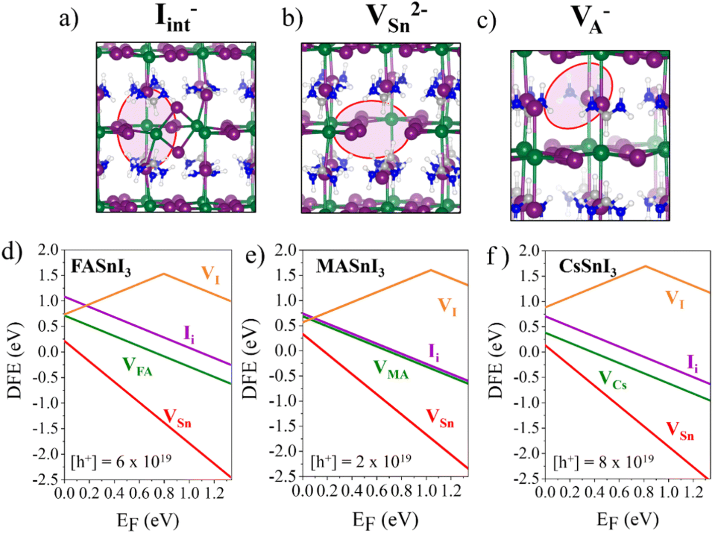 | ||
| Fig. 4 (a)–(c) Equilibrium structures of the modelled acceptor defects Ii−, VSn2−, and VA− in FASnI3; (d)–(f) defect formation energies of acceptor defects in the FASnI3, MASnI3 and CsSnI3 calculated in I-medium conditions at the HSE06 (0.43) level of theory by including DFT-D3 dispersions. Estimated hole densities are in cm−3. | ||
In Fig. 4d–f the calculated DFEs of these defects in I-medium conditions, simulating stoichiometric conditions of growth of the perovskites, are reported and compared with the DFEs of the VI donor defect. The three acceptor defects dominate the defect chemistry of the perovskites, with the tin vacancy being the most stable defect. By comparing the DFEs at the VBM, the VSn2− defect is slightly more stable in the Cs and FA phases compared to the MA perovskite, showing values of 0.13, 0.21 and 0.33 eV, respectively, see Table 1. Iodine interstitials, on the other hand, are more easily formed in the Cs and MA phases compared to FA, while vacancies of the inorganic Cs cation are more stable than organic FA and MA cations, showing comparable values. Overall, these results highlight that the heavy p-doping of the three perovskites can be equally ascribed to tin vacancies that pin the Fermi level close to the VBM with estimated hole densities of 6 × 10¹⁹, 2 × 10¹⁹ and 8 × 1019 cm−3 for the FA, MA and Cs perovskites. The slightly lower hole density predicted for the MASnI3 phase is in agreement with experimental observations.
| FASnI3 | MASnI3 | CsSnI3 | |
|---|---|---|---|
| VSn2− | 0.21 | 0.33 | 0.13 |
| Ii− | 1.02 | 0.74 | 0.71 |
| VA− | 0.71 | 0.68 | 0.38 |
Fig. S15 in ESI† shows the calculated DFEs of Sn vacancy, A+ cation vacancy and iodine interstitial defects under different growth conditions for FASnI3, MASnI3 and CsSnI3. Theoretical calculations indicate that under I-poor (Sn-rich) conditions the DFE of the Sn vacancy increases and the native Fermi level shifts up into the band gap due to the parallel stabilization of iodine vacancies and the formation of tin Frenkel pairs,35 independently from the nature of the A-site cation. Experimentally, this Sn-rich environment can be achieved by adding SnF2 to the precursor solution. As shown in Fig. S16,† the hole density decreases from 1019 to 1018 cm−3 with 10 mol% of SnF2 in both MASnI3 and CsSnI3, confirming that the reduction occurs regardless of the A-site cation. This trend is further supported by UV-vis, PL and PLQY measurements (Fig. S17 and S18†), where a redshift in the absorption onset and PL spectrum indicates a reduced Burstein–Moss effect and doping.36 Additionally, PLQY curves are no longer flat but instead increase with excitation density, revealing a trap filling process that further confirms reduced doping.24
Finally, considering that mixed A-site cation perovskites are widely employed in photovoltaics for both Pb- and Sn-based perovskites due to their enhanced performance, we investigated their effect on the optoelectronic properties of Sn halide perovskites. Fig. S19a–c in the ESI† present the top-view SEM images of FASnI3, FA0.85Cs0.15SnI3 and (FA0.85MA0.15)0.95Cs0.05SnI3 thin films, respectively. Substituting 15% of FA with Cs results in compact films with similar grain size to pristine FASnI3 but with a smoother morphology. Introducing both MA and Cs leads to larger grains but results in a less compact structure with numerous pinholes. As expected, incorporating Cs or MA into FASnI3 reduces the lattice parameter, leading to a redshift in the PL spectrum and a decrease in the bandgap (Fig. S19d†). Moreover, PL spectra of mixed-cation systems are narrower than that of FASnI3, indicating reduced disorder. Conductivity measurements (Fig. S19e†) reveal that the FACs Sn halide films exhibit values between those of FASnI3 and CsSnI3 films, while doping densities remain comparable to those of single-cation compositions (Fig. S19f†). DFT calculations show that alloying the A-site to form FA0.75Cs0.25SnI3 and FA0.75MA0.25SnI3 does not substantially alter the DFE of Sn vacancies, confirming that these systems remain heavily p-doped due to Fermi level pinning near the valence band maximum (Table S2†).
Conclusions
We investigated the role of single A-site cations on the properties of tin halide perovskite semiconductors, focusing on how the cation influences the defect chemistry and the p-doping level. We find that the electrical conductivity of the films is highly dependent on the film morphology. More compact films with larger grains demonstrated higher effective charge carrier mobility and conductivity. The achievement of pin-hole free thin films, both via solution and vapor deposition, clearly shows a comparable density of free hole density, independent on the A cation. DFT calculations show that Sn vacancies, which are responsible for the intrinsic p-type doping in Sn perovskites, are the most stable defects across all compositions. Notably, different compositions show only little difference in Sn vacancy defect formation energies, correlating well with the experimental observation. The addition of SnF2, which creates a Sn-rich growth environment, uniformly reduces the doping level across the film, regardless of the nature of the A-site cation. These findings highlight the interplay between A-site cation selection, film morphology, and defect chemistry in determining the optoelectronic properties of tin halide perovskites, providing valuable guidelines for optimizing these materials for solar cell applications.Data availability
Data for this article are available at https://doi.org/10.5281/zenodo.14929702.Author contributions
IP and AP conceived and planned the experiments. EA and IP prepared, characterized and analysed solution based thin film materials. CB, LG, GB, DM and FDA performed DFT calculations. CP, DR, PDV, LVM and AA prepared, characterized and analysed vacuum-based thin film materials. CB and AT performed PLQY measurements. PR and MC performed electronic characterization of the films. IP and AP wrote the manuscript with support of all authors.Conflicts of interest
There are no conflicts to declare.Acknowledgements
The authors would like to thank Paolo Giavarini for initial support in the preparation and electrical characterization of the samples. This work has been funded by the European Union. Views and opinions expressed are however those of the author(s) only and do not necessarily reflect those of the European Union or CINEA. Neither the European Union nor the granting authority can be held responsible for them. VALHALLA project has received funding from Horizon Europe Research and Innovation Action programme under Grant Agreement n° 101082176. This work has also been funded by the European Union – NextGenerationEU, Mission 4, Component 2, under the Italian Ministry of University and Research (MUR) National Innovation Ecosystem grant ECS00000041 – VITALITY – CUP J97G22000170005 and CUP: B43C22000470005. We also acknowledge funding from the Italian Ministry of Environment and Energy Security in the framework of the Operating Agreement with ENEA for Research on the Electric System and of the Project GoPV (CSEAA_00011) for Research on the Electric System.Notes and references
- S. Min Park, M. Wei, J. Xu, H. R. Atapattu, F. T. Eickemeyer, K. Darabi, L. Grater, Y. Yang, C. Liu, S. Teale, B. Chen, H. Chen, T. Wang, L. Zeng, A. Maxwell, Z. Wang, K. R. Rao, Z. Cai, S. M. Zakeeruddin, J. T. Pham, C. M. Risko, A. Amassian, M. G. Kanatzidis, K. R. Graham, M. Grätzel and E. H. Sargent, Science, 2023, 381, 209–215 Search PubMed.
- W. Peng, K. Mao, F. Cai, H. Meng, Z. Zhu, T. Li, S. Yuan, Z. Xu, X. Feng, J. Xu, M. D. McGehee and J. Xu, Science, 2023, 379, 683–690 CAS.
- S. Tao, I. Schmidt, G. Brocks, J. Jiang, I. Tranca, K. Meerholz and S. Olthof, Nat. Commun., 2019, 10, 1–10 CAS.
- A. Amat, E. Mosconi, E. Ronca, C. Quarti, P. Umari, M. K. Nazeeruddin, M. Grätzel and F. De Angelis, Nano Lett., 2014, 14, 3608–3616 CAS.
- Q. Lin, S. P. Senanayak, N. Yaghoobi Nia, M. Alsari, S. Lilliu and M. Abdi-Jalebi, Energy Technol., 2023, 11, 2300358 CAS.
- F. Ünlü, E. Jung, J. Haddad, A. Kulkarni, S. Öz, H. Choi, T. Fischer, S. Chakraborty, T. Kirchartz and S. Mathur, APL Mater., 2020, 8, 070901 Search PubMed.
- Q. Lin, D. J. Kubicki, M. K. Omrani, F. Alam and M. Abdi-Jalebi, J. Mater. Chem. C, 2023, 11, 2449–2468 CAS.
- F. Xu, T. Zhang, G. Li and Y. Zhao, J. Mater. Chem. A, 2017, 5, 11450–11461 CAS.
- E. Aktas, N. Rajamanickam, J. Pascual, S. Hu, M. H. Aldamasy, D. Di Girolamo, W. Li, G. Nasti, E. Martínez-Ferrero, A. Wakamiya, E. Palomares and A. Abate, Commun. Mater., 2022, 3, 104 CAS.
- B. Yu, Z. Chen, Y. Zhu, Y. Wang, B. Han, G. Chen, X. Zhang, Z. Du and Z. He, Adv. Mater., 2021, 33, 2102055 CAS.
- L. Ji, T. Zhang, Y. Wang, D. Liu, H. Chen, H. Zheng, X. Peng, S. Yuan, Z. D. Chen and S. Li, Nanoscale, 2022, 14, 1219–1225 CAS.
- T. Ye, X. Wang, K. Wang, S. Ma, D. Yang, Y. Hou, J. Yoon, K. Wang and S. Priya, ACS Energy Lett., 2021, 6, 1480–1489 CAS.
- R. Tounesi, L. H. Hernandez, L. Lanzetta, S. Jang, B. Davaasuren, M. A. Haque and D. Baran, ACS Appl. Electron. Mater., 2024, 6, 2826–2831 CAS.
- L. J. M. van de Ven, E. K. Tekelenburg, M. Pitaro, J. Pinna and M. A. Loi, ACS Energy Lett., 2024, 9, 992–999 CAS.
- M. Xiao, F. Huang, W. Huang, Y. Dkhissi, Y. Zhu, J. Etheridge, A. Gray-Weale, U. Bach, Y. B. Cheng and L. Spiccia, Angew. Chem., Int. Ed., 2014, 53, 9898–9903 CAS.
- M. S. Kirschner, B. T. Diroll, P. Guo, S. M. Harvey, W. Helweh, N. C. Flanders, A. Brumberg, N. E. Watkins, A. A. Leonard, A. M. Evans, M. R. Wasielewski, W. R. Dichtel, X. Zhang, L. X. Chen and R. D. Schaller, Nat. Commun., 2019, 10, 504 CAS.
- A. Treglia, M. Prato, C. S. J. Wu, E. L. Wong, I. Poli and A. Petrozza, Adv. Funct. Mater., 2024, 34, 2406954 CrossRef CAS.
- M. Pitaro, E. K. Tekelenburg, S. Shao and M. A. Loi, Adv. Mater., 2022, 34, 2105844 CrossRef CAS PubMed.
- Y. Dang, Y. Zhou, X. Liu, D. Ju, S. Xia, H. Xia and X. Tao, Angew. Chem., Int. Ed., 2016, 55, 3447–3450 CrossRef CAS PubMed.
- L. Peng and W. Xie, RSC Adv., 2020, 10, 14679–14688 RSC.
- M. Ozaki, Y. Katsuki, J. Liu, T. Handa, R. Nishikubo, S. Yakumaru, Y. Hashikawa, Y. Murata, T. Saito, Y. Shimakawa, Y. Kanemitsu, A. Saeki and A. Wakamiya, ACS Omega, 2017, 2, 7016–7021 CrossRef CAS PubMed.
- C. Quarti, E. Mosconi, J. M. Ball, V. D. Innocenzo, C. Tao, S. Pathak, H. J. Snaith and F. De Angelis, Energy Environ. Sci., 2016, 9, 155–163 RSC.
- R. L. Milot, M. T. Klug, C. L. Davies, Z. Wang, H. Kraus, H. J. Snaith, M. B. Johnston and L. M. Herz, Adv. Mater., 2018, 30, 1804506 CrossRef PubMed.
- A. Treglia, F. Ambrosio, S. Martani, G. Folpini, A. J. Barker, M. D. Albaqami, F. De Angelis, I. Poli and A. Petrozza, Mater. Horiz., 2022, 9, 1763–1773 RSC.
- S. Saini, A. K. Baranwal, T. Yabuki, S. Hayase and K. Miyazaki, MRS Adv., 2019, 4, 1719–1725 CrossRef CAS.
- F. Qian, M. Hu, J. Gong, C. Ge, Y. Zhou, J. Guo, M. Chen, Z. Ge, N. P. Padture, Y. Zhou and J. Feng, J. Phys. Chem. C, 2020, 124, 11749–11753 CrossRef CAS.
- H. Dong, C. Ran, W. Gao, N. Sun, X. Liu, Y. Xia, Y. Chen and W. Huang, Adv. Energy Mater., 2022, 12, 2102213 CrossRef CAS.
- W. Ning and F. Gao, Adv. Mater., 2019, 31, 1900326 CrossRef PubMed.
- G. Wang, J. Chang, J. Bi, M. Lei, C. Wang and Q. Qiao, Sol. RRL, 2022, 6, 2100841 CrossRef CAS.
- L. Monacelli and N. Marzari, Chem. Mater., 2023, 35, 1702–1709 CrossRef CAS PubMed.
- F. J. Berger, I. Poli, E. Aktas, S. Martani, D. Meggiolaro, L. Gregori, M. D. Albaqami, A. Abate, F. De Angelis and A. Petrozza, ACS Energy Lett., 2023, 8, 3876–3882 CrossRef CAS PubMed.
- Y. M. Lee, J. Park, B. D. Yu, S. Hong, M. C. Jung and M. Nakamura, J. Phys. Chem. Lett., 2018, 9, 2293–2297 CAS.
- I. Poli, G. Kim, E. L. Wong, A. Treglia, G. Folpini and A. Petrozza, ACS Energy Lett., 2021, 6, 609–611 CAS.
- J. Heyd, G. E. Scuseria and M. Ernzerhof, J. Chem. Phys., 2003, 118, 8207–8215 CAS.
- D. Meggiolaro, D. Ricciarelli, A. A. Alasmari, F. A. S. Alasmary and F. De Angelis, J. Phys. Chem. Lett., 2020, 11, 3546–3556 CrossRef CAS PubMed.
- K. J. Savill, A. M. Ulatowski and L. M. Herz, ACS Energy Lett., 2021, 6, 2413–2426 CrossRef CAS PubMed.
Footnote |
| † Electronic supplementary information (ESI) available. See DOI: https://doi.org/10.1039/d5el00010f |
| This journal is © The Royal Society of Chemistry 2025 |