
Enhanced mid-visible light absorption and long-lived charge carriers in an electronically and structurally integrated BiVO4–TiO2 photoanode for efficient artificial photosynthesis applications†
Vikas Kumar
Jha‡
a,
Kranti N.
Salgaonkar‡
bc,
Avishek
Saha
 *bc,
Chinnakonda S.
Gopinath
*bc and
E. Siva Subramaniam
Iyer
*a
*bc,
Chinnakonda S.
Gopinath
*bc and
E. Siva Subramaniam
Iyer
*a
aSchool of Chemical and Materials Sciences, Indian Institute of Technology Goa, Ponda, Goa, 403401, India. E-mail: essiyer@iitgoa.ac.in
bCatalysis and Inorganic Chemistry Division, CSIR-National Chemical Laboratory, Dr. Homi Bhabha Road, Pune, Maharashtra, 411008, India. E-mail: avi.saha.ncl@csir.res.in; cs.gopinath@ncl.res.in; csgopinaath@gmail.com
cAcademy of Scientific and Innovative Research (AcSIR), Ghaziabad 201002, India
First published on 22nd April 2025
Abstract
The ever-increasing demand for sustainable solutions for eliminating environmental pollutants, solar energy harvesting, water splitting, etc. have led to the design and development of novel materials to achieve the desired result. In this regard, structurally and electronically integrated (SEI) BiVO4–TiO2 (SEI–BVT) with abundant heterojunctions has emerged as a promising entity for efficient charge separation, which in turn enhances artificial photosynthesis (APS) activity. The present work adopted a unique synthetic strategy using SILAR to fabricate SEI–BVT from ionic precursors (Bi3+ and VO43−) into the pores of TiO2, exhibiting benchmark APS efficiency compared to the individual components. This preparation results in approximately 180 trillion uniformly distributed heterojunctions in 1 mg cm−2 of the SEI–BVT photoanode material. Charge carriers in SEI–BVT and BiVO4 are similar; however, the recombination is highly hindered when SEI–BVT heterojunctions are formed in the former. Our earlier work demonstrated 31–38% solar-to-fuel efficiency (STFE) with BiVO4–TiO2 for APS in the presence of the Pd-nanocube co-catalyst. The emphasis of the current work is to explore the dynamics of the light-induced processes in these heterojunctions to understand the interfacial charge transfer process. Femtosecond transient absorption (TA) spectroscopy has been employed to monitor the excited state dynamics. Our results show that new trap states have evolved under light illumination, which are significantly long-lived and hinder charge recombination, and consequently enhance STFE. A significantly large number of charge carriers exhibit a lifetime of ≫6 ns with visible light photons, at least up to 720 nm, which is higher than the band-gap absorption onset at 490 nm for SEI–BVT compared to bulk BiVO4. The rate of formation of charge carriers is significantly affected in the heterojunctions.
 Avishek Saha | Dr. Avishek Saha is a scientist at CSIR–National Chemical Laboratory (NCL), Pune, India. He received his B.Sc. from the University of Calcutta (2006) and M.Sc. from IIT Bombay (2008), followed by a Ph.D. from Rice University, USA (2013). He has done postdoctoral research at the University of Erlangen–Nuremberg, Germany, and Los Alamos National Laboratory, USA (2013–2018). He began his independent research career at CSIR–Central Scientific Instruments Organisation (CSIO), Chandigarh, in 2018, and later joined CSIR–NCL in 2023. Dr. Saha has co-authored over 35 peer-reviewed publications. His research focuses on heterogeneous photocatalysis and nanocarbon-based hybrids for catalytic and optical sensing applications. |
Introduction
Semiconductor-based photocatalysis and electrocatalysis for water splitting, the CO2 reduction reaction (CRR) and biomass-upgradation have gained immense attention in the last ten years owing to their ability to utilize naturally abundant solar energy.1,2 Nonetheless, the major challenge that humanity faces is global warming due to the excessive use of conventional carbon-containing fossil fuels.3,4 Rapid urbanisation and industry are necessary evils that also contribute to environmental pollution. Therefore, it is essential to find the necessary solutions to eliminate such pollutants. By 2035, the annual carbon dioxide emissions alone will be more than forty gigatons.5 Several approaches are employed to convert CO2 to value-added chemicals like methanol, ethanol, and formic acid. In this regard, photocatalytic conversion and artificial photosynthesis (APS) appear to be sustainable approaches.6 Over the years, several research groups have sought to improve solar harvesting using semiconductor materials.7–10 The photocatalytic efficiency primarily depends on light absorption by the material, the extent of charge recombination of the generated excitons, and surface reactions involving the charge carriers that do not recombine within the reaction time scales.6 Any high efficiency photocatalysts prepared for such applications must be tested for these properties for better exploitation.The photocatalytic properties of titania, owing to its practical applications in water splitting, photo-induced electron transfer, air purification, etc., have been extensively studied to understand its excited state dynamics.11–15 However, the use of titania is limited due to its wide band gap (Eg = 3.2 eV), resulting in the absorption being limited to the UV part of solar radiation. The efficiency of the photocatalytic material is further governed by the electron–hole dynamics after light absorption. Earlier studies have indicated that the trapped holes absorb at ∼500 nm in the mid-visible range, while the electrons absorb around 700 nm.16,17 The excited state dynamics in TiO2 are complex and the electrons and holes are distributed in various kinds of trapping sites. Yoshihara and co-workers studied nanocrystalline films of TiO2, where the dynamics were separated into free electrons and trapped electrons.13 This work showed that the trapped species, including trapped holes, were distributed on the surface while the free electrons were distributed in the bulk. The recombination of free electrons and holes was observed to occur in microsecond timescales, while the recombination of surface electrons with holes occurred within a few nanoseconds.13 Ultrafast transient spectroscopic measurements on nanocrystalline TiO2 have revealed that the surface electrons decay into deep traps within 0.5 ns.15 In order to improve the efficiency of titania, several methods have been employed.14,16,18–21 Integrating TiO2 with another semiconducting material giving rise to heterojunctions has emerged as a potential and promising method to improve the catalytic efficiency of TiO2.22–24
Bismuth vanadate (BiVO4), owing to light absorption from the mid-visible portion of the solar spectrum, exhibits a band gap of 2.35 eV (530 nm).25,26 This value is just below the reduction potential for water, making it a promising candidate for water oxidation, which is the critical requirement and first step of APS. Bismuth-based materials have gained attraction due to their resistance to corrosion, non-toxicity, water oxidation capability, and reasonably good dispersibility.27–31 However, BiVO4 suffers from poor surface catalytic activity. Recently, Salgaonkar et al. have reported a successive ionic layer adsorption and reaction (SILAR) approach to obtain a structurally and electronically integrated BiVO4–TiO2 (denoted as SEI–BVT or BVT) photoanode with a few hundred trillions of heterojunctions. This material exhibits type II heterojunctions.2 It has been demonstrated that the BiVO4–TiO2 heterojunctions achieved using the SILAR approach exhibited high activity for the CO2 reduction reaction (CRR), with BiVO4 being the primary source of the visible light absorber in SEI–BVT. The device performance remained largely unchanged over a large photoanode area (9 cm2) too. In our earlier work, we suggested that multiple band gaps are possible due to the distribution of BiVO4 quantum dots (BV QDs) of different sizes (1.5–6 nm), which results in broad absorption of visible light. We also semi-quantitatively calculated the existence of a large number of nano-heterojunctions in SEI–BVT. These heterojunctions are directly responsible for charge carrier separation, which in turn enhances solar-to-fuel efficiency (STFE) (31–38%) of APS. CRR experiments, indeed, underscore an efficient charge separation at the heterojunctions.32
BiVO4 is known to have complex carrier dynamics that occur in multiple stages.33,34 Kennis and co-workers have suggested that a fraction of photogenerated holes are trapped in less than 200 fs, while a more significant fraction of holes are trapped over 5 ps. The photo-excited electrons exhibit much longer dynamics. The excited electrons undergo relaxation over the first 40 ps, followed by forming trap-states over the next few nanoseconds. The charge recombination is suggested to occur over much longer timescales up to a few microseconds.35 The hole decay process is shown to be affected when heterostructures of BiVO4 with metal oxides like WO3 are prepared. In such systems, the internal decay within BiVO4 is hampered, resulting in long-lived charge-separated states.36 The heterojunctions of SEI–BVT composites formed using hydrothermal methods have been shown to have enhanced photocatalytic oxidation activity towards the degradation of organic dyes.32 There have been very limited reports that have investigated the dynamics of charge carriers in SEI–BVT composites. For example, a work by Hess et al. reported that physical charge separation yields extremely long-lived photoexcited states, which in turn enhances the photoelectrochemical functionality;37 however, a TiO2 (NR-nanorod)–BiVO4 composite was prepared by mixing, followed by centrifugation and spin-coating on FTO to a thickness of 200 nm. In the present work, we have studied the dynamics of BVT prepared by the SILAR method using femtosecond transient absorption spectroscopy. The SILAR process results in a large number of quantum dots of BiVO4 inside the micro and mesopores of titania, which in turn results in 180 trillion heterojunctions. Studying the interfacial charge transfer across heterojunctions in a structurally and electronically integrated composite would help synthesize photocatalytic materials with better performance. To this end, through ultrafast spectroscopic investigations, we notice that newer electronic states are generated at the interface of heterojunctions, resulting in broader absorption of the solar spectrum, which is otherwise limited for TiO2. Furthermore, it has been shown that the excited state dynamics of SEI–BVT are not affected by the thickness of the material, reflecting the possibility of increased scalability to prepare photoanodes for practical applications.
Experimental
Materials and methods
![[thin space (1/6-em)]](https://www.rsc.org/images/entities/char_2009.gif) :1 ratio. Similarly, 25 mM NH4VO3 solution was prepared by dissolving the required ammonium metavanadate in water at 348 K. The former and latter solutions are the sources of cations and anions, respectively, and they were employed in the SILAR method to assemble Bi3+ and VO3− ions in the pores of TiO2. A pre-coated TiO2 film on FTO, prepared using the standard doctor-blade method, was immersed in Bi(NO3)3 solution for 20 s; this was followed by subsequent immersion in NH4VO3 solution maintained at 348 K for 20 s. This was followed by washing with deionized water to remove any weakly held precursor ions. All three steps together are considered as one SILAR cycle. The amount/size of BV QDs in the titania pores gradually increased as the number of SILAR cycles subjected increased; in particular, 10 SILAR cycles were applied on the TiO2 film, exhibiting the maximum activity of the device. However, for the present dynamics studies, 2 and 10 SILAR cycles were applied on different thicknesses of TiO2 films, namely 4, 6, and 10 μm, and evaluated. After the required SILAR cycles, the film was annealed in air at 723 K for 2 h to form uniform BV QDs in the pores of TiO2. This procedure leads to the SEI–BVT photoanode device. 1 cm2 of the SEI–BVT device contains 1 mg of photoanode material; 2.5 ± 0.3 wt% BiVO4 QDs are present in the pores of 97 ± 5 wt% TiO2. It is to be noted that more than the required number of SILAR cycles leads to the deposition of BiVO4 on the exterior surface, which would lead to agglomeration. To completely avoid this, the 4 and 6 μm thick films were subjected to 2 SILAR cycles, while the 10 μm TiO2 film was subjected to 10 SILAR cycles.
:1 ratio. Similarly, 25 mM NH4VO3 solution was prepared by dissolving the required ammonium metavanadate in water at 348 K. The former and latter solutions are the sources of cations and anions, respectively, and they were employed in the SILAR method to assemble Bi3+ and VO3− ions in the pores of TiO2. A pre-coated TiO2 film on FTO, prepared using the standard doctor-blade method, was immersed in Bi(NO3)3 solution for 20 s; this was followed by subsequent immersion in NH4VO3 solution maintained at 348 K for 20 s. This was followed by washing with deionized water to remove any weakly held precursor ions. All three steps together are considered as one SILAR cycle. The amount/size of BV QDs in the titania pores gradually increased as the number of SILAR cycles subjected increased; in particular, 10 SILAR cycles were applied on the TiO2 film, exhibiting the maximum activity of the device. However, for the present dynamics studies, 2 and 10 SILAR cycles were applied on different thicknesses of TiO2 films, namely 4, 6, and 10 μm, and evaluated. After the required SILAR cycles, the film was annealed in air at 723 K for 2 h to form uniform BV QDs in the pores of TiO2. This procedure leads to the SEI–BVT photoanode device. 1 cm2 of the SEI–BVT device contains 1 mg of photoanode material; 2.5 ± 0.3 wt% BiVO4 QDs are present in the pores of 97 ± 5 wt% TiO2. It is to be noted that more than the required number of SILAR cycles leads to the deposition of BiVO4 on the exterior surface, which would lead to agglomeration. To completely avoid this, the 4 and 6 μm thick films were subjected to 2 SILAR cycles, while the 10 μm TiO2 film was subjected to 10 SILAR cycles.
The same SILAR procedure was also employed to prepare the bulk BiVO4 film, but directly on a plain FTO plate. 10 SILAR cycles were applied on an FTO plate with precursor solutions of Bi3+ and metavanadate. This was followed by drying at 333 K and air-calcination at 723 K for 2 h. Although the BiVO4 film could be made using the SILAR method directly on an FTO plate, the thickness of the film was observed to be ∼1.5 μm, and hence the advantage of preparing QDs in TiO2 mesopores could not be achieved.
Characterization
Diffuse reflectance UV–vis measurements were performed using a Shimadzu spectrophotometer (model UV-2550). Powder X-ray diffraction (XRD) data were obtained using a Pan Analytic X′pert Pro dual goniometer diffractometer, employing Cu–Kα (1.5418 Å) radiation with a Ni filter. Field emission scanning electron microscopy (FESEM) and energy dispersive spectroscopy (EDS) were performed using an FEI NOVA NANOSEM 450 FESEM system equipped with an EDS detector. The pore volume and pore size distribution were determined using nitrogen adsorption isotherms at 77 K recorded using a Quadrasorb for physisorption (Quantachrome) instrument.The incident photon-to-current efficiency (IPCE) measurements were conducted using a two-electrode setup with an electrochemical analyzer. The sample was employed as the photoanode; a platinum foil was the reference electrode. The photoanode was deposited on a fluorine-doped tin oxide (FTO) substrate. The IPCE measurement was performed using a Newport solar simulator (UUX 1404565) in CO2-saturated water at 25 °C, using a monochromator for specific wavelengths.
Results and discussion
Assembling and integrating BiVO4 quantum dots in nanopores of TiO2 – TEM-HRTEM characterization
TEM analysis was carried out with the SEI–BVT material to explore the textural properties, particularly the containment of BV QDs in TiO2 pores and the inevitable heterojunctions among them. Representative TEM images recorded are shown in Fig. 1. While bare TiO2 shows uniform grey contrast particles (not shown), SEI–BVT shows a number of TiO2 pores filled with BV QDs; the dark contrast underscores the assembled BV QDs in the mesopores of titania. Indeed, assemblies of BV QDs are observed uniformly in the TiO2 mesopores indicating their distribution over the entire thickness of the film. The HRTEM images show that BV QDs are spherical in shape with particle size ranging, predominantly, between 1.5 and 5.0 nm. HRTEM demonstrates type-II heterojunction formation between BV QDs and TiO2 due to the confinement of the former in the micro and mesopores of the latter. The uniqueness of the SILAR method appears to be similar to that of nature, in which the atomic/ionic assembly occurs by facilitating the diffusion of the ionic precursors, and the high energy of inner surfaces of pores helps in assembling a monolayer of cations and anions in the pores for each SILAR cycle. In fact, XRD of TiO2 with assembled ionic precursors is no different from TiO2. Only on air calcination at 723 K, BV features appear in XRD, and ensure the assembly of BV QDs in the TiO2 pores. BV QDs show a d-spacing of 0.308 nm corresponding to the highly abundant (121) facet (Fig. 1b). TiO2 particles display the abundantly available inter-planar distance (d = 0.35 nm), corresponding to the (101) facet of anatase. TEM studies fully support the diffusion of ionic precursors (Bi3+ and VO3−) into the pores of TiO2 and thus BiVO4 QD formation on calcination. BiVO4–TiO2 heterojunctions observed over the entire film thickness help in electron–hole separation as well as the dispersion of electrons to the cathode, through the bottom FTO plate. The N2 adsorption–desorption isotherms of SEI–BVT and TiO2 materials exhibit a type-IV adsorption–desorption isotherm (Fig. S1†). The BET results (Fig. S1a†) of P25–TiO2 (BVT) show a surface area and pore volume of 58 (54) m2 g−1 and 0.18 (0.16) ml g−1. According to the pore size distribution, pore volume is primarily contributed by mesopores (>2 nm) and to a lesser extent by micropores (<2 nm) in both cases. A significant and notable reduction in the pore volume for SEI–BVT, compared to TiO2, is observed, which is attributed to the BV QDs occupying the pores. In addition, a clear decrease in the extent of micro and mesopores is observed in pore size distribution, which fully supports the pore-filling by BV QDs in the TiO2 host matrix. | ||
| Fig. 1 (a) TEM image of the SEI–BVT photoanode material at the 20 nm scale bar. (b) HRTEM image of SEI–BVT at the 2 nm scale bar exhibits the confined BiVO4 QDs in TiO2 mesopores and abundant heterostructures formed between them. The dark contrast and d-spacing confirm the presence of assembled BiVO4 in grey contrast TiO2. | ||
HAADF-STEM image and elemental analyses (Fig. S2†) provide further evidence of incorporation of BiVO4 quantum dots in the pores of TiO2 films. As shown in the elemental mapping, the BiVO4 quantum dots are evenly distributed, especially on the pores as well as at the edges and outer surfaces of the titania particles. Additionally, there is a slightly lower density of BV-QDs within the larger TiO2 particles. The distribution of BV-QDs is most noticeable in Fig. S2 (panel b).† These findings align well with the TEM and HRTEM results.
UV-visible absorption spectroscopy was employed to evaluate the optical absorption characteristics of TiO2 (10 μm), SEI–BVT and bulk BVT, and the spectra are shown in Fig. 2(a). No significant changes were observed in the UV-vis spectra of TiO2 films of different thicknesses. It is well known that TiO2 absorbs exclusively in the UV region with no absorption from the visible region. Bulk BiVO4 exhibits an absorption edge at ∼530 nm (Eg = 2.35 eV), while the same is observed at 490 nm with the SEI–BVT photoanode, corresponding to Eg = 2.53 eV. The bandgap increased significantly for SEI–BVT due to the quantum confinement of BV QDs in the pores of TiO2, as evident from HRTEM (Fig. 1). In addition, a notable color change from greenish yellow for bulk BiVO4 to bright yellow for SEI–BVT was observed (Fig. S3†). These observations indicate that BiVO4 and TiO2 are electronically integrated into one BVT composite photoanode material. The data support the notion that the ionic precursor components (Bi3+ and VO3−) of BiVO4 diffuse into the TiO2 pores due to the SILAR method. Post-calcination, these precursors convert to BV QDs within the TiO2 pores. The embedding of QDs ensures the formation of heterojunctions with a core–shell morphology, potentially involving BiVO4 protrusions into TiO2, thus indicating electronic as well as structural integration.
 | ||
| Fig. 2 (a) UV-visible absorption spectra of bulk TiO2, BiVO4 and SEI–BVT (BiVO4–TiO2) photoanodes. Note a blue shift in the absorption onset after the integration of BiVO4 in TiO2 pores. (b) Powder X-ray diffraction of bulk BiVO4, TiO2 and SEI–BVT (BiVO4–TiO2) photoanodes. | ||
The powder X-ray diffraction (XRD) spectra are consistent with previous reports, where a shift in the (121) plane (2θ = 28.85°) of bulk BiVO4 was observed in SEI–BVT, as shown in Fig. 2(b). This shift generally suggests lattice compression along the (121) facet of BiVO4. X-ray photoelectron spectroscopy (XPS) analysis revealed that only V5+ is present in SEI–BVT, while both V5+ and V4+ are detected in bulk BiVO4 (Fig. S4 in the ESI†). This finding suggests that charge transfer occurs from BiVO4 to the TiO2 lattice, facilitating efficient charge transfer. No significant changes were observed in the core-level binding energies (BEs) of Ti 2p3/2 (458.7 eV) and Bi 4f7/2 (159 eV) between BVT and BiVO4.
A wireless artificial photosynthesis device made with SEI–BVT as the photoanode and Pd-nanocubes coated as a co-catalyst, designated as BVT–APS was used to assess the photocatalytic CRR. The experimental conditions included evaluation under one sun conditions, both under laboratory settings and direct sunlight exposure. Experiments were performed with CO2-saturated water in the presence of direct sunlight in a batch reactor, and product analysis was carried out periodically using HPLC. Product yields observed as a function of illumination time are shown in Fig. 3a. Interestingly, the only carbon-containing liquid products detected were formaldehyde (HCHO) and methanol (MeOH). No other carbon-containing liquid or gaseous products, such as CO, formic acid (HCOOH), methane (CH4), or hydrogen (H2), were found. After a 5 hour reaction period under direct sunlight using a 1 cm2 BVT–APS device, the cumulative yields of HCHO and MeOH were found to be 358 and 281 μmol, respectively. Table ST1† summarizes the products from the batch mode CRR under direct sunlight for 5 hours. Repeatability of the yield was observed throughout several batches within ±10% error margin. Notably, 38% of the initially dissolved CO2 was converted into solar fuel or chemicals within the 5 hour timeframe, indicating a first-order reaction kinetics based on a linear evolution of CO2 conversion and product selectivity. While the total yield of both products increased, the ratio of MeOH:HCHO also increased as a function of illumination time, suggesting a gradual increase in the conversion of CO2 to products, and sequential hydrogenation of CO2 to HCHO and subsequently to MeOH. This phenomenon highlights the possibility of optimizing reaction parameters to generate methanol selectively. Furthermore, the only oxidation product was found to be oxygen (O2), with a yield of 8.3 μmol h−1 cm2, which was significantly less than the expected stoichiometric amount in comparison with the reduction products.
 | ||
| Fig. 3 (a) Photocatalytic CRR activity and CO2 conversion rate observed with a 1 cm2 SEI–BVT APS device under direct sunlight for 5 h. (b) The wavelength-dependent incident photon-to-current efficiency (IPCE) performance of photoanodes compared to the SEI–BVT absorption range. Inset shows the photocatalytic CRR activity comparison under direct sunlight irradiation conditions for TiO2, BiVO4 and SEI–BVT. The total amount of C1-oxygenates observed with SEI-BVT is at least 20 times higher than that observed with BiVO4 alone, underscoring the importance of material integration aspects; TiO2 does not show any C1-oxygenates. | ||
Batch-type CRR conditions, utilizing CO2-saturated water, were used for the IPCE measurements at 298 K, without any applied potential, and the results are shown in Fig. 3b. Notably, the IPCE values for the SEI–BVT photoanode significantly surpass those of the bulk BiVO4 photoanode across the entire visible light spectrum. Above 550 nm, the IPCE value for the BVT photoanode remains constant at 8%. Bulk BiVO4 shows IPCE values around 6.5% up to 440 nm, which rapidly decreases at longer wavelengths to 0 at 520 nm. It is important to note that pure/bulk BiVO4, prepared using the SILAR method, has a large particle size of ∼400 (±100) nm (Fig. S5, ESI†) with low IPCE values above 440 nm due to high charge carrier recombination. A huge increase in the IPCE values from 13% (at 460 nm) to 31% (at 410 nm) indicates that smaller BV QDs contribute significantly to the photocurrent generation and also to the overall CRR activity. It is very likely that the micropores are filled in the first few SILAR cycles with BV QDs, followed by the filling of mesopores. Smaller BV QDs result in higher IPCE values, suggesting that micropores of 1–2 nm diameter, with significantly larger band gaps, are filled. This is supported by the visible light absorption by SEI–BVT, as shown in Fig. 3b. The CRR activity obtained with SEI–BVT, BiVO4, and TiO2 photoanodes with Pd-nanocubes as the co-catalyst under one sun conditions are shown in the inset of Fig. 3b. High IPCE values highlight effective charge separation and diffusion over macroscopic distances for SEI–BVT photoanodes, contributing to higher CRR activity than those of BiVO4 and TiO2. More details about the reaction aspects are available in our earlier report.2
Time-resolved spectroscopy investigations
TiO2-coated fused silica absorbs strongly throughout the UV and visible regions. The transmission of probe light through uncoated fused silica and the samples coated with TiO2 of varying thicknesses is shown in Fig. S6.† The samples are opaque for wavelengths less than 480 nm. As a result, all the measurements have been reported beyond the probe wavelength of 480 nm. Although colloidal dispersions of titania are known to absorb only in the ultraviolet region, the present film materials are considerably thick and absorb even the longer wavelengths. The dynamics of TiO2 are monitored by pumping at 380 nm. Fig. 4 displays the wavelength-dependent kinetic traces at varying thicknesses of the TiO2 films. The 4 μm thick TiO2 film exhibits stimulated emission at wavelengths less than 500 nm. The spectra are dominated by strong positive signals beyond 500 nm. The kinetic traces between 500 and 620 nm show a prominent rise, followed by the decay of excited state absorption. Meanwhile, the kinetic traces at redder wavelengths only exhibit decay. The stimulated emission is not observed with 6 and 10 μm thick TiO2 films because of a lack of data at the corresponding wavelengths. Nevertheless, a prominent slow rise in the excited state absorption was observed in all the cases. It is interesting to note that in the 4 μm thick titania, the slow initial rise observed at wavelengths less than 620 nm is absent beyond 650 nm, where only decay is observed (Fig. 4a). However, the 10 μm TiO2 continues to show the initial slow rise even at longer wavelengths. The kinetic traces beyond 20 ps time scales overlap for all the three samples irrespective of the thickness (Fig. S7,†Table 1). All our measurements have been carried out at sufficiently low energies to subdue higher-order electron–hole recombination processes.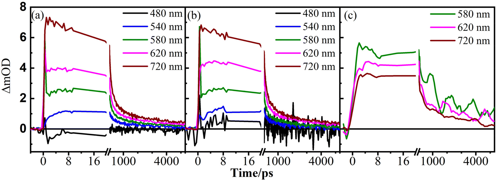 | ||
| Fig. 4 The transient kinetic traces for TiO2 with different thicknesses, namely (a) 4 μm, (b) 6 μm, and (c) 10 μm, at different probe wavelengths. The samples are pumped at 380 nm. | ||
| Sample | Thickness | λ pump | λ probe | τ 1/ps | τ 2/ps | τ 3/ns | τ 4/ns |
|---|---|---|---|---|---|---|---|
| a Lifetime is kept fixed during the fitting procedure. Lifetimes reported in bold have negative amplitudes. The kinetic parameters at other representative wavelengths are presented in Fig. S11–S18 and Tables ST2–ST5.† | |||||||
| TiO2 | 4 μm | 380 | 480 | 4.9 ± 0.3 | — | — | — |
| 540 | 2.4 ± 1.1 | 125 ± 67 | 1.0 ± 0.2 | — | |||
| 600 | — | 116 ± 3.7 | 1.4 ± 0.07 | — | |||
| 720 | — | 83 ± 2.8 | 0.9 ± 0.05 | — | |||
| 6 μm | 540 | 3.7 ± 1.9 | 150 ± 59 | 2.2 ± 1.2 | — | ||
| 600 | 1.0 ± 1.1 | 119 ± 11 | 1.5 ± 0.2 | — | |||
| 720 | — | 88 ± 2.7 | 1.2 ± 0.4 | — | |||
| 10 μm | 540 | 4.7 ± 2.3 | 200a | 1.6 ± 0.9 | — | ||
| 600 | 5.0 ± 2.1 | 200 ± 110 | 2.0 ± 0.8 | — | |||
| 720 | 5.0 ± 3.9 | 200 ± 74 | 2.0 ± 0.8 | — | |||
| BiVO4 | 1.5 μm | 380 | 480 | 3.5 ± 0.6 | 200 ± 150 | — | Long lived |
| 540 | 5.0 ± 1.2 | 200a | — | Long lived | |||
| 600 | 6.0 ± 1.6 | 200a | — | Long lived | |||
| 720 | 6.0 ± 5.4 | 200 ± 186 | — | Long lived | |||
| 1.5 μm | 450 | 540 | 3.2 ± 2.8 | — | — | Long lived | |
| 600 | 4.7 ± 1.9 | — | — | Long lived | |||
| 720 | 6 ± 4 | — | — | ||||
| SEI–BVT | 4 μm | 380 | 550 | 1.0 ± 0.3 | 43 ± 19 | 1.8 ± 0.2 | Long lived |
| 720 | 1.2 ± 0.1 | 33 ± 4 | 1.5 ± 0.3 | Long lived | |||
| 6 μm | 550 | 1.2 ± 1.0 | 47 ± 25 | 1.9 ± 1.2 | Long lived | ||
| 720 | 2.0 ± 0.4 | 30a | 1.0 ± 0.3 | Long lived | |||
| 10 μm | 550 | 1.4 ± 0.4 | 50 ± 27 | 2a | Long lived | ||
| 720 | 2.0 ± 0.4 | 30 ± 10 | 1.4 ± 0.7 | Long lived | |||
| 4 μm | 450 | 550 | — | 30 ± 15 | 0.5 ± 0.3 | Long lived | |
| 720 | 1.5 ± 0.3 | 26 ± 5 | 0.6 ± 0.1 | Long lived | |||
| 6 μm | 550 | 2.6 ± 0.2 | 46a | 0.5a | Long lived | ||
| 720 | 1.6 ± 0.3 | 28 ± 6 | 0.8 ± 0.3 | Long lived | |||
| 10 μm | 720 | 3.0 ± 2.9 | 50 ± 30 | 0.8 ± 0.5 | Long lived | ||
The sub-nanosecond processes in titania are governed by the relaxation of surface charge carriers and trapped electrons that migrate within the nanoparticles.15,38 The spectral signatures are manifested as stimulated emission at the bluer wavelengths and the excited state absorption takes place in similar time scales. They can be assigned to the generation of the surface carriers. The stimulated emission has been ascribed to charge recombination, while the absorption to the holes. The formation of charge carriers is followed by the migration of the generated carriers. The excited state absorption between 500 and 800 nm can be associated with this process. A slower rise in the absorption band for the thick 10 μm film can be explained on the basis of slower migration of the surface-trapped electrons and holes. Meanwhile, in the thinner films, the charge migration process is sufficiently fast. As a result, only a fast and slow decay is noticed in the thin films at longer wavelengths. The rates observed for generating charge carriers and recombining electrons and holes are similar to those reported in earlier works.15,38 The 5 and 40 ps components are assigned to intra-band electron relaxation and hole migration. The slowest process beyond 200 ps is usually ascribed to the recombination of the electrons and holes. This process is invariant with the thickness of titania. This is not unusual since the recombination process is governed by the band gap in TiO2, which is not expected to differ in the samples with varying thicknesses. Hence, it may be summarised that the charge carriers are formed within a few hundred femtoseconds in titania. However, the migration of the holes and electrons depends on the thickness of TiO2 due to the deep traps that can be present in thicker samples. Meanwhile, the recombination of the electrons and holes is independent of the material thickness.
The excited state dynamics of BiVO4 films are monitored by pumping at two different wavelengths, namely 380 (UV) and 450 nm (visible). The kinetic traces at a few representative wavelengths are shown in Fig. 5. The lower energy, 450 nm, excitation matches closely the band gap of BiVO4. This results in populating the lowest levels of the conduction band. The transient spectra reveal only negative bands across the wavelengths probed. A negative band at longer wavelengths in a transient absorption spectrum is associated with stimulated emission. The normalised kinetic traces at different probe wavelengths overlap with each other, indicating that the entire negative band originates from the same state (Fig. S8†). The amplitude of these signals is very low, suggesting that a very small population is excited at this wavelength. The transient absorption spectra from the two experiments, i.e. by exciting at 380 nm and 450 nm, are shown in Fig. S9.† When excited at 380 nm, BiVO4 exhibits a broad excited state absorption throughout the probed region. The decays are invariant across the probe wavelengths. Representative decays at a few wavelengths across the spectra are shown in Fig. 5a. The decays can be characterized by two distinct features: a short sub 10 ps increase followed by decay with a lifetime of ∼200 ps that evolves to a long-lived state that does not decay within the measurement time of the instrument. The lifetimes obtained are in similar scales reported in earlier works on thin films of BiVO4.33,34 The short component is assigned to the electron relaxation to the bottom of the conduction band while the long nanosecond component is attributed to the electron–hole recombination process.35 Thus, pumping at a higher energy than the band gap results in states that decay to long-lived deep traps, eventually leading to electron–hole recombination processes. Such deep traps are not formed when BiVO4 is excited to lower levels by the 450 nm pump.
 | ||
| Fig. 5 The transient absorption kinetic traces of bulk BiVO4 at different probe wavelengths when pumped at (a) 380 nm and (b) 450 nm. | ||
Having monitored the dynamics of TiO2 and BiVO4 independently, we probed the dynamics of the heterojunctions in SEI–BVT. The heterojunctions resulting from the SILAR method are monitored by pumping at two different wavelengths, 380 nm, and 450 nm, corresponding to the direct excitation of TiO2 and BiVO4, respectively. It is observed that the kinetic traces post-excitation at 450 nm are independent of the thickness of the SEI–BVT film (Fig. 6); a similar observation is made when pumped at 380 nm. This suggests that the nature of heterojunctions is the same irrespective of the thickness of the materials under study. It is worthwhile to note that thin films of TiO2 exhibited wavelength-dependent kinetics, while thicker samples did not (Fig. 4). Meanwhile, BiVO4 did not exhibit a wavelength-dependent dynamics change when excited at the band edge but did show dependence when excited much above the band edge (Fig. 6). The reasons are explained in the preceding paragraph.
 | ||
| Fig. 6 Normalised kinetic traces of SEI–BVT of different thicknesses (4 μm: black, 6 μm: green, and 10 μm: blue circles) at 580, 620 and 720 nm with excitation by the pump at (a–c) 380 nm and (d–f) 450 nm. | ||
The dynamics observed for the heterojunctions present in the SEI–BVT material are distinctly different from those of individual components (Fig. 4 and 5), suggesting the formation of new states that can affect the photocatalytic properties of the materials. The transient kinetics at a few representative wavelengths by pumping the material at 380 nm and their comparison with those of TiO2 and BiVO4 are provided in Fig. 7. The most noteworthy feature is the formation of new long-lived states in the thin-layered (4 and 6 μm) samples. Compared to bare TiO2, where the formation of charge carriers is ultrafast, in the case of the SEI–BVT with abundant heterojunctions, this appears to slow down. It also underscores a significantly slower decay process within 10 ps post excitation with SEI–BVT. This sub-10 ps process is followed by a long decay whose amplitude is significantly higher than that of TiO2; this is especially important, given the predominant amount of TiO2 (≥97%) in SEI–BVT. These timescales correspond to the charge carrier migration through titania, which appears to slow down in the presence of heterojunctions in SEI–BVT. As the films become thick (10 μm; Fig. 7h and i), the long-time decay, beyond 1 ns, matches those of bare TiO2. Hence, it may be inferred that bulk-like features of TiO2 become prominent as the samples become thick. A similar exercise is carried out for samples pumped at 450 nm. Since bare TiO2 does not give any transient spectra at this excitation, a comparison with TiO2 cannot be done.
 | ||
| Fig. 7 Comparison of kinetic traces of TiO2 (blue), BiVO4 (black), and SEI–BVT (green) at different probe wavelengths and pumped at 380 nm for 4 μm (a–c), 6 μm (d–f) and 10 μm (g–i) thick layers of the nanocomposite. The 10 μm thick TiO2 is opaque to the probe at 550 nm and hence not shown in (g). | ||
Fig. 8 compares the dynamics of the heterojunctions in SEI–BVT with bulk BiVO4. The most striking difference noted is that BiVO4 exhibited only negative signals in the transient spectra, while the heterojunctions have only positive signals. For comparison, the stimulated emission decays of BiVO4 have been multiplied by −1 and overlaid with the decays of SEI–BVT (Fig. 8). It should be emphasized at this stage that very weak stimulated emission was noticed for bulk BiVO4 (Fig. S9†) compared to the strong excited state absorption when BiVO4 was excited higher than the band gap. It is likely that in heterojunctions, the excited state absorption is much stronger than that of stimulated emission, which is not apparent in the data. It is observed that the traces up to 4 ps are nearly similar. This observation becomes more apparent at the redder wavelengths and in thicker samples (cf.Fig. 8c, f and i). It is to be reiterated that no positive signals were observed from bulk BiVO4 and the kinetic trace at the respective wavelength is multiplied by −1 for overlay and comparison with SEI–BVT. Beyond this time, the decay of the excited state absorption is not completed within the time scales of our measurements (Table 1). Meanwhile, the stimulated emission approaches near zero within 2 ns. Hence, excitation at 450 nm generates the charge carriers in SEI–BVT similar to that of BiVO4; however, the recombination is highly hindered when heterojunctions are formed. The particle size of BiVO4 (400 ± 100 nm; Fig. S5†) in bare BiVO4 is much larger than that of SEI–BVT; the latter exhibits the size of BV QDs in the order of a few nanometers. This is manifested in the form of the intermediate lifetime component over 1–2 ns in SEI–BVT. This new state can be attributed to the slower charge migration on the surface of SEI–BVT. The bulk BiVO4 does not exhibit such a state because the charge recombination occurs on a much faster timescale. This new state can explain the enhanced IPCE, which increases fivefold and exhibits around 30% efficiency (Fig. 3b). The fast lifetime of 30–50 ps in SEI–BVT can be assigned to the recombination of trapped holes and excited free electrons, whereas the 1 ns process is attributed to the recombination of trapped holes and trapped electrons. The fast process is invariant with the sample thickness; thus, it may be inferred that such a recombination is localised to heterojunctions only. Since the number of heterojunctions in SEI–BVT per sq cm is in trillions, the effect is multi-fold, and a high increment in IPCE current is noticed. The invariance in lifetimes of the fast process with the thickness of the material has been observed earlier with the WO3/BiVO4 material as well.36 In WO3/BiVO4, it was predicted that the photogenerated holes live longer. Our experiments with SEI–BVT show a similar feature. This aspect enhances the first step of water splitting to produce protons and electrons, which is essential for CO2 reduction. The same conclusions can be arrived at when the material was excited at the wavelength at which TiO2 shows strong absorbance. The effect of excitation wavelengths on the heterojunction films is shown in Fig. S10.† It is readily observed that the late-time profiles beyond a nanosecond are nearly overlapping and independent of the pump wavelength. This indicates that the same long-lived state is attained irrespective of how the carriers are generated (Table 1). Based on the experiments presented in this work, we conclude that the formation of heterojunctions results in the formation of newer states that absorb well in the mid-visible regions. The schematics of the excited state process are depicted in Fig. 9. The valence bands of BiVO4 lie above TiO2; consequently the charge carriers can easily migrate retarding the recombination processes. These newly formed states are long-lived and, as a result, improve their catalytic efficiency. Furthermore, the BV QDs in SEI–BVT have marginally higher band gaps than bulk BiVO4, as seen from the absorption curves (Fig. 2a) and substantiated by the transient absorption measurements where a strong positive band in the mid-visible wavelength range is observed due to intra-band transitions. Indeed, this is the main reason for observing the 7% IPCE current, even at wavelengths between 520 and 700 nm, and possibly above 700 nm (Fig. 3b).
 | ||
| Fig. 8 Comparison of kinetic traces of BiVO4 (black) and SEI–BVT (green) at different probe wavelengths and pumped at 450 nm for 4 μm (a–c), 6 μm (d–f), and 10 μm (g–i) thick layers of the nanocomposite. It is to be noted that the BiVO4 data have been multiplied by −1 for better visualization and comparison. | ||
 | ||
| Fig. 9 Schematic representation of the excited state process in SEI–BVT heterojunctions. | ||
Long-lived charge-separated states, along with a different and prolonged relaxation process observed with SEI–BVT, make the holes available for water oxidation. Indeed, this is the critical and most sluggish step in water activation to molecular oxygen and simultaneous proton formation. Under the current APS experimental conditions, CO2 dissolved in the molecular form in water is available, and it readily reacts with protons to form carbonic acid. This is confirmed from the observation of a decrease in pH to about 5–5.5 under experimental running conditions. Up to 30% IPCE shown in Fig. 3b demonstrates the injection of electrons from BV QDs into TiO2 in SEI–BVT. These observations underscore the efficient utilization of holes for water oxidation and electrons for reduced products of CO2 to methanol and formaldehyde.
Conclusions
The BiVO4–TiO2 SEI–BVT films prepared using the SILAR technique, containing 97.5 wt% TiO2 and 2.5 wt% BiVO4 QDs in the pores of the former result in the formation of abundant heterojunction structures. The interaction between the energy levels of the two semiconductors gives rise to newer states thereby generating a significantly large number of charge carriers resulting in a retarded charge recombination process leading to long-lived charge separated states. The formation of charge carriers in the SEI–BVT material due to absorption of photons seems to occur in a similar manner irrespective of individual components. However, the relaxation processes are highly altered. The relaxation processes are shown to continue for several nanoseconds. These long-lived states could be the primary reason for the enhanced photocatalytic efficiency of the SEI–BVT material. Analysis of such engineered photocatalysts is likely to lead to a better understanding of the role of heterojunctions in charge separation. The current work also underscores that electronic and structural integration of individual components of composite photocatalysts is essential for improving their overall activity.Author contributions
VKJ carried out the spectroscopic investigations and analysed the TAS results. KNS prepared and characterised the samples. All authors conceived the idea and wrote the manuscript.Data availability
The data supporting this article have been included as part of the ESI.†Conflicts of interest
There are no conflicts to declare.Acknowledgements
VKJ thanks IITGOA for a fellowship. KNS thanks CSIR for a fellowship. CSG acknowledges the financial support from CSIR through the HCP-44 project. AS and CSG further acknowledge financial support from the Tata Consulting Engineers (TCE) Ltd., CSR grant (CSR000226).References
- (a) C. S. Gopinath and N. Nalajala, J. Mater. Chem. A, 2021, 9, 1353–1371 RSC; (b) N. Nalajala, K. K. Patra, P. A. Bharad and C. S. Gopinath, RSC Adv., 2019, 9, 6094–6100 RSC; (c) K. K. Patra and C. S. Gopinath, Chem. Commun., 2023, 59, 6774–6795 RSC; (d) T. R. Nivedhitha, H. Bajpai, J. O. Varghese, A. Abraham, I. Chauhan and C. S. Gopinath, ACS Sustainable Chem. Eng., 2024, 12, 14841–14853 CrossRef CAS; (e) I. Chauhan, H. Bajpai, B. Ray, S. K. Kolekar, S. Dattar, K. K. Patra and C. S. Gopinath, ACS Appl. Mater. Interfaces, 2024, 16, 26130–26141 CrossRef CAS PubMed.
- (a) K. N. Salgaonkar, H. Bajpai, N. N. Mhamane, N. Nalajala, I. Chauhan, K. Thakkar, K. Joshi and C. S. Gopinath, J. Mater. Chem. A, 2023, 11, 15168–15182 RSC; (b) N. Nalajala, K. N. Salgaonkar, I. Chauhan, S. Mekala and C. S. Gopinath, ACS Appl. Energy Mater., 2021, 4, 13347–13360 CrossRef CAS.
- S. R. Lingampalli, M. M. Ayyub and C. N. R. Rao, ACS Omega, 2017, 2, 2740–2748 CrossRef CAS PubMed.
- J. Ran, M. Jaroniec and S.-Z. Qiao, Adv. Mater., 2018, 30, 1704649 CrossRef PubMed.
- S. N. Habisreutinger, L. Schmidt-Mende and J. K. Stolarczyk, Angew. Chem., Int. Ed., 2013, 52, 7372–7408 CrossRef CAS PubMed.
- (a) V. Kumaravel, J. Bartlett and S. C. Pillai, ACS Energy Lett., 2020, 5, 486–519 CrossRef CAS; (b) C. S. Gopinath and K. N. Salgaonkar, WO Patent, 2022/044039A1, 2022 Search PubMed.
- (a) D. Cui, W. Hao and J. Chen, ChemNanoMat, 2021, 7, 894–901 CrossRef CAS; (b) K. K. Patra, B. D. Bhuskute and C. S. Gopinath, Sci. Rep., 2017, 7, 6515 CrossRef PubMed; (c) M. Mapa, K. Sivaranjani, D. S. Bhange, B. Saha, P. Chakraborty, A. K. Viswanath and C. S. Gopinath, Chem. Mater., 2010, 22, 565–578 CrossRef CAS.
- (a) K. Xie, N. Umezawa, N. Zhang, P. Reunchan, Y. Zhang and J. Ye, Energy Environ. Sci., 2011, 4, 4211–4219 RSC; (b) H. Bajpai, I. Chauhan, K. N. Salgaonkar, N. B. Mhamane and C. S. Gopinath, RSC Sustainability, 2023, 1, 481–493 RSC.
- (a) D. Jiang, Y. Zhou, Q. Zhang, Q. Song, C. Zhou, X. Shi and D. Li, ACS Appl. Mater. Interfaces, 2021, 13, 46772–46782 CrossRef CAS PubMed; (b) P. Devaraji and C. S. Gopinath, Int. J. Hydrogen Energy, 2018, 43, 601–613 CrossRef CAS; (c) P. A. Bharad, A. V. Nikam, F. Thomas and C. S. Gopinath, ChemistrySelect, 2018, 3, 12022–12030 CrossRef CAS; (d) K. Sivaranjani, S. Agarkar, S. B. Ogale and C. S. Gopinath, J. Phys. Chem. C, 2012, 116, 2581–2587 CrossRef CAS.
- (a) L. Ye, Y. Deng, L. Wang, H. Xie and F. Su, ChemSusChem, 2019, 12, 3671–3701 CrossRef CAS PubMed; (b) S. Rajaambal, M. Mapa and C. S. Gopinath, Dalton Trans., 2014, 43, 12546–12554 RSC; (c) P. A. Bharad, K. Sivaranjani and C. S. Gopinath, Nanoscale, 2015, 7, 11206–11215 RSC; (d) H. Bajpai, K. K. Patra, R. Ranjan, N. Nalajala, K. P. Reddy and C. S. Gopinath, ACS Appl. Mater. Interfaces, 2020, 12, 30420–30430 CrossRef CAS PubMed.
- (a) A. Fujishima, T. N. Rao and D. A. Tryk, J. Photochem. Photobiol., C, 2000, 1, 1–21 CrossRef CAS; (b) S. S. Mani, S. Rajendran, T. Mathew and C. S. Gopinath, Energy Adv., 2024, 3, 1472–1504 RSC.
- A. Fujishima, K. Hashimoto and T. Watanabe, TiO2 photocatalysis: Fundamentals and applications, BKC Inc, Tokyo, 1st edn, 1999 Search PubMed.
- (a) T. Yoshihara, R. Katoh, A. Furube, Y. Tamaki, M. Murai, K. Hara, S. Murata, H. Arakawa and M. Tachiya, J. Phys. Chem. B, 2004, 108, 3817–3823 CrossRef CAS; (b) A. A. Melvin, K. Illath, T. Das, T. Raja, S. Bhattacharyya and C. S. Gopinath, Nanoscale, 2015, 7, 13477–13488 RSC.
- A. J. Cowan, J. Tang, W. Leng, J. R. Durrant and D. R. Klug, J. Phys. Chem. C, 2010, 114, 4208–4214 CrossRef CAS.
- Y. Tamaki, A. Furube, M. Murai, K. Hara, R. Katoh and M. Tachiya, Phys. Chem. Chem. Phys., 2007, 9, 1453–1460 RSC.
- P. V. Kamat, Chem. Rev., 1993, 93, 267–300 CrossRef CAS.
- D. W. Bahnemann, M. Hilgendorff and R. Memming, J. Phys. Chem. B, 1997, 101, 4265–4275 CrossRef CAS.
- J. B. Ashbury, E. Hao, Y. Wang, H. N. Ghosh and T. Lian, J. Phys. Chem. B, 2001, 105, 4545–4557 CrossRef.
- S. Rajaambal, K. Sivaranjani and C. S. Gopinath, J. Chem. Sci., 2015, 127, 33–47 CrossRef CAS.
- (a) K. K. Patra, P. A. Bharad, V. Jain and C. S. Gopinath, J. Mater. Chem. A, 2019, 7, 3179–3189 RSC; (b) H. Bajpai, T. R. Nivedhitha, E. Dais, S. S. Kanungo and C. S. Gopinath, J. Catal., 2024, 437, 115644 CrossRef CAS.
- F. C. Soares, J. C. de Almeida, R. H. Koga, D. M. da Silva Del Duque, G. T. S. T. da Silva, C. Riberio and V. R. de Mendonca, Mater. Chem. Phys., 2022, 290, 126588 CrossRef CAS.
- S. J. A. Moniz, S. A. Shevlin, D. J. Martin, Z.-X. Guo and J. Tang, Energy Environ. Sci., 2015, 8, 731–759 RSC.
- B. Tudu, N. Nalajala, K. P. Reddy, P. Saikia and C. S. Gopinath, ACS Sustainable Chem. Eng., 2021, 9, 13915–13925 CrossRef CAS.
- G. Qiu, T. Wang, X. Li, X. Tao and B. Li, Ind. Eng. Chem. Res., 2020, 59, 11517–11526 CrossRef CAS.
- B. J. Trzeesniewski and W. A. Smith, J. Mater. Chem. A, 2016, 4, 2919–2926 RSC.
- A. Malathi, J. Madhavan, M. Ashokkumar and P. Arunachalam, Appl. Catal., A, 2018, 555, 47–74 CrossRef CAS.
- M. Guo, Y. Wang, Q. He, W. Wang, W. Wang, Z. Fu and H. Wang, RSC Adv., 2015, 5, 58633–58639 RSC.
- D. Lv, D. Zhang, X. Pu, D. Kong, Z. Lu, X. Shao, H. Ma and J. Dou, Sep. Purif. Technol., 2017, 174, 97–103 CrossRef CAS.
- Y. Hu, J. Fan, C. Pu, H. Li, E. Liu and X. Hu, J. Photochem. Photobiol., A, 2017, 337, 172–183 CrossRef CAS.
- G. S. Kamble and Y.-C. Ling, Sci. Rep., 2020, 10, 12993 CrossRef CAS PubMed.
- M. Ganeshbabu, N. Kannan, P. S. Venkatesh, G. Paulraj, K. Jegannathan and D. M. Ali, RSC Adv., 2020, 10, 18315 RSC.
- S. Mansaour, R. Akkar, S. B. Chaabene and M. S. Zina, Adv. Mater. Sci. Eng., 2020, 6505301 CrossRef.
- J. K. Cooper, S. E. Reyes-Lillo, L. H. Hess, C.-M. Jiang, J. B. Neaton and I. D. Sharp, J. Phys. Chem. C, 2018, 122, 20642–20652 CrossRef CAS.
- A. Kahraman, M. B. Vishlaghi, I. Baylam, A. Sennaroglu and S. Kaya, J. Phys. Chem. C, 2019, 123, 28576–28583 CrossRef CAS.
- J. Revensbergen, F. F. Abdi, J. H. van Santen, R. N. Frese, B. Dam, R. van de Krol and J. T. M. Kennis, J. Phys. Chem. C, 2014, 118, 27793–27800 CrossRef.
- I. Grigoni, A. Polo, M. V. Dozzi, K. G. Stamplecoskie, D. H. Jara, P. V. Kamat and E. Selli, ACS Appl. Energy Mater., 2022, 5, 13142–13148 CrossRef PubMed.
- L. H. Hess, J. K. Cooper, A. Loiudice, C.-M. Jiang, R. Buosanti and I. D. Sharp, Nano Energy, 2017, 34, 375–384 CrossRef CAS.
- Y. Tamaki, A. Furube, M. Murai, K. Hara, R. Katoh and M. Tachiya, J. Am. Chem. Soc., 2006, 128, 416–417 CrossRef CAS PubMed.
Footnotes |
| † Electronic supplementary information (ESI) available: Nitrogen adsorption–desorption isotherms and pore size distribution (S1), STEM and EDS (S2), digital photograph (S3), XPS spectra (S4), SEM image of bulk BiVO4 (S5), probe spectra (S6), normalized transient absorption kinetics of TiO2 (S7) and BiVO4 (S8), transient absorption of BiVO4 (S9), pump–probe thickness dependent kinetics (S10), thickness dependent kinetics traces of TiO2 (S11–S13), kinetic traces of BiVO4 (S14 and S15), kinetic traces of SEI–BVT (S16–S18), summary of CO2 reduction reaction products (Table ST1), and kinetic fitting parameters of TiO2, BiVO4, and SEI–BVT (Tables ST2–ST5). See DOI: https://doi.org/10.1039/d5nr00723b |
| ‡ These authors contributed equally to this work. |
| This journal is © The Royal Society of Chemistry 2025 |