
 Open Access Article
 This Open Access Article is licensed under a Creative Commons Attribution-Non Commercial 3.0 Unported Licence
Additive-assisted molecular aggregation manipulation towards efficient thick organic solar cells†
Xueting
Yi
ab,
Zekun
Liu
ab,
Mengan
Zhao
ab,
Minghui
Huang
ab,
Jiang
Wu
ab,
Yingying
Fu
*a and
Zhiyuan
Xie
 *ab
*ab
aState Key Laboratory of Polymer Physics and Chemistry, Changchun Institute of Applied Chemistry, Chinese Academy of Sciences, Changchun 130022, P. R. China. E-mail: fyy@ciac.ac.cn; xiezy_n@ciac.ac.cn
bSchool of Applied Chemistry and Engineering, University of Science and Technology of China, Hefei 230026, P. R. China
First published on 26th September 2024
Abstract
Developing thickness-insensitive organic solar cells (OSCs) is of vital importance for meeting the requirements of the mass production of solar panels. Herein, the molecular aggregation behaviour of non-fullerene acceptors was manipulated via two different solvent additives, namely, 1-phenylnaphthalene (PN) and 1-chloronaphthalene (CN), to improve the charge transport in thick OSCs. The planar structure of the naphthalene ring coupled with large phenyl steric hindrance allows the PN additive to insert into the adjacent N3 molecules, disturbing their face-to-face π–π stacking and enhancing the J-aggregation in the blends. As a result, the PN-treated blend film exhibits red-shifted and broad absorption as well as increased charge carrier mobility, which is crucial for high-performance thick OSCs. In contrast, the CN additive, with a small side group possessing good solubility for N3 and a high boiling point, facilitates the H-type aggregation of acceptors in the spin-coating process. With the incorporation of 0.5 vol% PN, the 120-nm-thick D18-Cl:N3-based devices obtained a power conversion efficiency (PCE) over 18.0%, significantly higher than the 16.22% and 16.08% for the control and CN-treated devices, respectively. Impressively, when the active layer thickness is increased to 300 nm, the resultant device still obtained a PCE of 16.48%. This work provides a simple additive strategy to facilitate the precise control of molecular aggregation during the film formation process for high-performance thick OSCs.
Introduction
Organic solar cells (OSCs) have garnered extensive attention in the realm of energy conversion technology because of their advantages of low-cost processing, flexibility and compatibility with large-area roll-to-roll manufacturing.1–4 A power conversion efficiency (PCE) of about 19% has been achieved in recent years, credited to advancements in novel donor and acceptor materials as well as device engineering optimization, signifying significant strides towards their commercial application.5–11 However, most efficient OSCs are typically fabricated with a thin active layer of 100–120 nm, which limits sufficient light harvesting and tends to form spot defects in scaled up manufacturing, leading to serious efficiency loss. In addition, the poor tolerance poses a critical challenge for roll-to-roll printing due to the inevitable thickness fluctuation during high-throughput manufacturing processes.12–16 To address these issues and broaden the processing window for large-scale production, an active layer with thickness extended to several hundreds of nanometers could be more advantageous.16–19 Unfortunately, a thick active layer often leads to dramatic PCE reduction resulting from its unfavourable morphology and low mobility, causing a dilemma between the active layer thickness and device efficiency.20–23To improve the performance of thick active layer OSCs, considerable efforts have been devoted to material development as well as device engineering, such as the synthesis of temperature-dependent aggregative polymers,24 the employment of layer-by-layer approach,17 and the introduction of fullerene liquid crystal into the active layer.25 An effective strategy for thick-film regulation should ensure excellent crystallinity, optimal aggregation and superior vertical phase separation for efficient charge transport and collection.26 Among these methods, the use of solvent additives within the active layer is deemed a convenient and effective approach for morphology regulation in thin-film OSCs.5 Nevertheless, the impact of solvent additives on the device performance of thick-film OSCs is still less understood. On the other hand, the molecular aggregation of donors and/or acceptors plays a pivotal role in film morphology and charge mobility in the active layers. In particular, non-fullerene acceptors (NFAs) usually form H- or J-aggregation, facilitating the building of a three-dimensional (3D) interpenetrated network structure that is conducive to realizing efficient charge transport in multiple directions.27 Both molecular structures and processing conditions strongly affect the stacking behaviour during film formation. It is found that suitable additives can significantly promote the aggregation of non-fullerene small molecules, resulting in improved charge mobility in the bulk heterojunction (BHJ) films.28 Although solvent additives have been widely used in highly efficient organic photovoltaics, their impacts on the aggregation kinetics are quite complicated and not clear enough. For a specific system, the selection of solvent additives is usually based on trial and error since the volatility, solubility and interaction with NFAs backbone or substituents potentially have a profound influence on the stacking styles of conjugated small molecules. It is still a challenge to develop an additive-choosing criterion for manipulating the molecular aggregation and regulating the film morphology.
Herein, we introduced two solvent additives with different steric hindrance, namely, 1-phenylnaphthalene (PN) and 1-chloronaphthalene (CN), to explore their influence on molecular aggregation and crystallization behaviour, charge transport and device performance in D18-Cl:N3-based OSCs. It is found that the addition of PN promotes J-aggregation since large steric hindrance from phenyl substituents disturbs the face-to-face π–π stacking of N3 molecules. In contrast, CN-treated films prefer to form H-type aggregation, which could be attributed to the small side group of CN. Although both PN and CN additives can improve the crystallization of N3 molecules due to the increased J- or H-type stacking, PN-treated films exhibit more favourable morphology with enhanced crystalline coherence length (CCL) in the D18-Cl:N3 blends. Compared to the D18-Cl:N3 devices with the CN additive, the OSCs processed with PN additive show higher carrier mobility, higher charge collection efficiencies and reduced charge recombination. Meanwhile, the increased J-aggregation of N3 molecules in PN-treated D18-Cl:N3 blends is conducive to broaden the absorption spectra, resulting in an increased photocurrent. Benefitting from the enhanced charge transport and collection efficiency as well as the improved photon harvesting capability, a PCE of 18.0% is achieved for the PN-treated OSC devices with a 120 nm-thick D18-Cl:N3 active layer, significantly higher than that of the control (16.22%) and CN-treated (16.08%) devices, respectively. Moreover, the OSCs based on the 300 nm-thick PN-treated D18-Cl:N3 active layer still demonstrate an outstanding PCE of 16.48%, together with a short-circuit current density (JSC) of 27.69 mA cm−2, open-circuit voltage (VOC) of 0.83 V, and fill factor (FF) of 71.98%. In contrast, the control and CN-treated devices with the same active layer thickness obtain moderate PCEs of 14.23% and 14.34%, respectively.
Results and discussion
The chemical structures of the polymer donor D18-Cl, non-fullerene acceptor N3, and solvent additives PN and CN are depicted in Fig. 1(a). With regards to the CN additive, PN has a large phenyl substituent that may induce distinct steric hindrance effects on the crystallization kinetics during the spin-coating process, thereby altering the molecular packing of donors or acceptors. To verify this hypothesis, we first investigated the optical properties of neat and blend films prepared with PN or CN additive. As shown in Fig. 1(b), the D18-Cl films processed without and with different additives exhibit similar UV-Vis absorption spectra from 450 to 600 nm, indicating the negligible impact of PN or CN on the polymer arrangement. However, the status is completely different for N3. As shown in Fig. 1(c), the pristine N3 film without any additives shows a primary absorption peak at 823 nm and a shoulder peak at 759 nm, which is assigned to the 0–0 and 0–1 vibronic transitions, respectively. The 0–0 peak of 0.5 vol% PN-treated N3 film undergoes a significant red-shift of about 22 nm and the 0–1 peak intensity (I0–1) concurrently displays a proportional decrease, implying the enhanced J-aggregation of the N3 molecules. In contrast, the absorption of the 0.5 vol% CN-processed N3 film is dramatically blue-shifted by about 67 nm with a lower ratio of I0–0/I0–1, which suggests dominant H-aggregation in CN-treated N3 films. In addition, the PN-treated N3 films exhibit much broader absorption spectra with a full width at half maximum (FWHM) of 256 nm compared to the pristine and CN-treated N3 films, which is favourable for enhancing the photocurrent. This phenomenon was also observed in the PM6:Y6 blends processed with the solid additive and was attributed to the disturbed molecular packing of the acceptors caused by the solid additive.28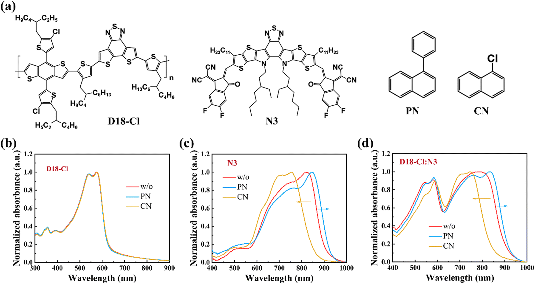 | ||
| Fig. 1 (a) Chemical structures of D18-Cl, N3 and solvent additives PN and CN. (b)–(d) The absorbance of neat D18-Cl, neat N3 and D18-Cl:N3 blend films without and with different additives (0.5 vol%). | ||
Compared to the neat N3 films, the absorption spectra of the D18-Cl:N3 blends in Fig. 1(d) show the similar trend that PN-treated films exhibit an obvious red-shifted absorption while CN-treated ones are blue-shifted, which is attributed to the disparate aggregation behaviours of N3 in the blend films processed with different additives. Notably, D18-Cl:N3 blend films exhibit blue-shifted absorption compared to the corresponding pristine N3 films that could be ascribed to the restricted molecular motion of small molecules in the polymer donor matrix, thus contributing to the formation of H-type aggregation.29 The influence of additive concentration on molecular stacking is shown in Fig. S1 (ESI†). With the increased concentrations of PN or CN, both neat N3 and D18-Cl:N3 blend films demonstrate gradually red- or blue-shifted absorption spectra, indicating a gradual increase of J- or H-aggregation in the films. The use of additives represents a strategy to modulate the aggregation types, with the varied effects depending on the specific molecules involved.29–31 In N3-based systems, it can be concluded that J- and H-aggregation coexist while PN and CN are conducive to the dominant formation of J- and H-aggregation of N3, respectively. The different effects of PN and CN solvent additives on the molecular packing of N3 can be attributed to the distinct steric hindrance aroused by their substituents. A series of other naphthalene derivatives with various substituents were further employed as additives to confirm the impact of substituent hindrance effects on N3 molecular stacking. As shown in Fig. S2 (ESI†), the N3 films processed with 1,1′-binaphthalene additive show significantly red-shifted absorption peaks while the 1-methylnaphthalene, 1-methoxynaphthalene and 1-fluoronaphthalene-treated ones exhibit blue-shifted absorption spectra. Since 1-methylnaphthalene has similar polarity as PN, the blue-shifted absorption in the 1-methylnaphthalene-treated N3 film further confirms that it is the steric hindrance rather than the polarity of additives that significantly influences the aggregation behaviours of the N3 acceptors. Furthermore, Fourier transform infrared (FTIR) spectroscopy was employed to verify whether PN was removed, and the results are shown in Fig. S3 (ESI†). The additive PN exhibits two characteristic peaks at 3055 cm−1 and 1494 cm−1 corresponding to the C–H stretching vibration and aromatic ring skeleton deformation vibration, respectively. In the PN-treated N3 films, these characteristic peaks could be clearly observed, indicating that the additive still remains in the film after spin-coating due to its high boiling point. However, the characteristic peaks of PN disappear completely, implying that PN is effectively removed after spin-coating methanol treatment. Some other studies have also demonstrated that methanol treatment can remove the additives effectively.32–34
Grazing incidence X-ray diffraction (GIXRD) measurements were performed to investigate the impact of additives on the molecular crystallinity in neat and blend films. The corresponding scattering profiles are compared in Fig. 2 and Fig. S4 (ESI†), and detailed quantitative analyses are summarized in Tables S1 and S2 (ESI†). The neat D18-Cl films without additives show a (010) π–π stacking peak along the out-of-plane (OOP) direction at qz = 1.679 Å−1 and a pronounced lamellar peak at qxy = 0.292 Å−1 along the in-plane (IP) direction in Fig. S4 (ESI†). The corresponding diffraction positions are unchanged for the D18-Cl films processed with PN or CN additives, indicating that both additives can hardly affect the polymer packing behaviours. In Fig. 2(a), the neat N3 film exhibits strong π–π stacking in the OOP direction and lamellar stacking in the IP direction due to their preferential face-on orientation with respect to the substrates. Compared to the pristine N3 film, the intensity of the π–π stacking peak for the PN- and CN-treated N3 films are significantly increased, implying better crystallinity and higher degree of molecular ordering. Meanwhile, the (010) diffraction peak at qz = 1.797 Å−1 in the PN-incorporated N3 films demonstrates closer π–π stacking among the N3 molecules. As depicted in Fig. 2(b), the D18-Cl:N3 blend film processed with 0.5 vol% PN shows a more pronounced (100) lamellar diffraction peak at qxy = 0.281 Å−1 and (010) π–π stacking peak at qz = 1.787 Å−1. The crystalline correlation lengths (CCLs) of the D18-Cl:N3 films were calculated from the GIXRD profiles using Scherrer's equation,35 and the results are plotted in Fig. 2(c). Compared to the blend film without the additive, the CCLs associated with lamellar stacking peaks in the CN- and PN-incorporated blend films were improved from 25.89 Å to 31.08 Å and 31.47 Å, respectively, manifesting increased crystalline domains in the blend films. Simultaneously, the CCLs derived from the π–π stacking peak were boosted from 20.13 Å to 25.55 Å, indicating an enhanced π–π ordering induced by the addition of PN. Additionally, the slightly decreased d-spacing in the OOP direction shown in Fig. 2(d) demonstrates the positive effect of PN in promoting the regular and compact π-stacking of N3 molecules in the blend films. The significant improvement of the molecular packing and crystallinity aroused by the PN additive is beneficial for charge transport in the resultant OSCs.
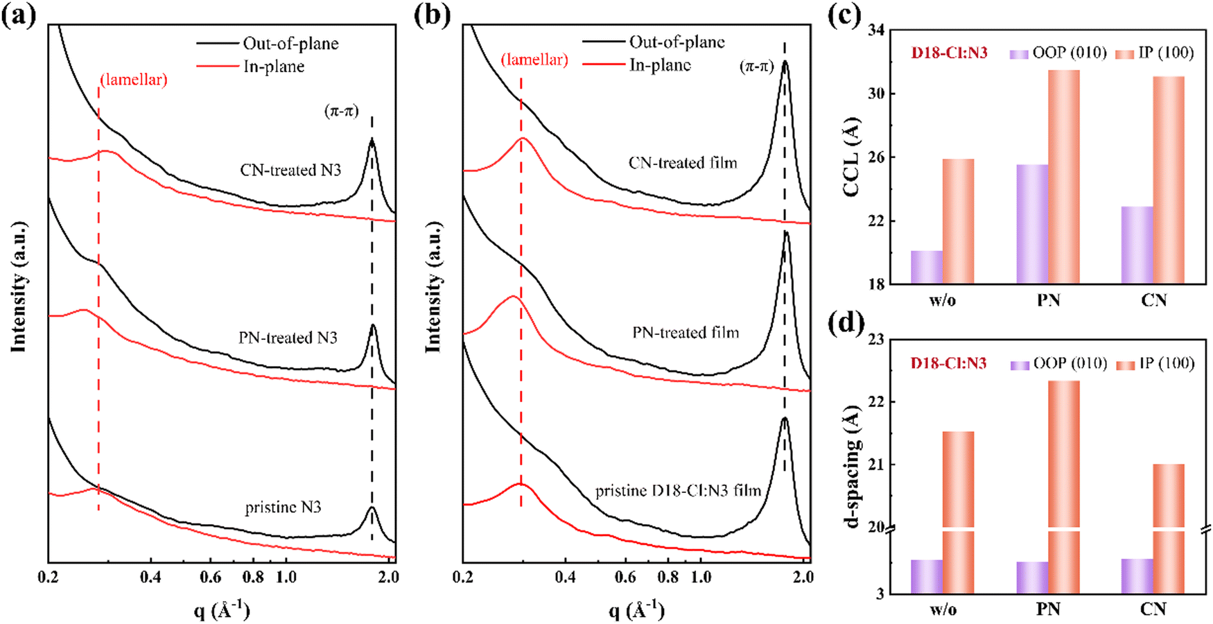 | ||
| Fig. 2 (a) and (b) The GIXRD profiles of neat N3 and D18-Cl:N3 blend films without and with different additives (0.5 vol%). (c) The calculated CCLs and (d) d-spacing variation in the D18-Cl:N3 blend films without and with different additives (0.5 vol%). | ||
The atomic force microscopy (AFM) images of various films are depicted in Fig. S5–S8 (ESI†). The D18-Cl films show quite a smooth surface, and the root mean square (RMS) roughness marginally increased even with the volume fraction of PN or CN additives up to 2%. However, the neat N3 films processed with 2 vol% PN and CN additives show significantly increased RMS from 1.47 nm to 7.48 nm and 23.1 nm, respectively. These results validate again that the PN and CN additives primarily manipulate the aggregation of N3. The D18-Cl:N3 blend films processed with 0.5 vol% PN or CN form uniform nanofibril network structures, which are beneficial to exciton dissociation and charge transport. In detail, the RMS of 0.5% additive-processed films were slightly increased compared with the control film, which is attributed to the more ordered aggregation behaviour of the acceptors. When the CN additive is increased to 2 vol%, it will induce an abrupt expansion of phase separation, accompanied by the emergence of large-sized N3 aggregates. In comparison, a relatively small RMS of 2.57 nm is achieved in the D18-Cl:N3 film processed with 2 vol% PN, possibly implying the superior concentration tolerance of PN additives.
The formation process from the solution to the film state was further explored via in situ UV-Vis absorption spectra, as shown in Fig. 3(a)–(c), providing a comprehensive understanding of the drying and crystallization dynamics in D18-Cl:N3 blends. The characteristic absorption peak position and the intensity of the donors and acceptors were plotted as a function of spin-coating time in Fig. 3(d)–(f), respectively. According to previous reports,36 the process can be divided into four temporal stages: (i) the fast removal of solution by centrifugal force, where only the absorption intensity drops quickly, but the peak position rarely changes; (ii) the evaporation of the main solvent persists while the additive remains in the “wet” film; (iii) the aggregation and crystallization of donors and/or acceptors, evidenced by either peak red shifting or absorbance improvement; (iv) film formation is eventually completed. During the whole spin-coating process, D18-Cl in all the three samples exhibits almost identical and constant peak positions due to similar pre-aggregation in solutions. The quickly increased peak intensity of D18-Cl at about 0.97–1.09 s mainly contributes to its high crystallization rate, which is not influenced by the additives. In the third stage of 0.92–1.25 s in Fig. 3(d), a non-monotonic transition is detected for the 0–0 peak position of N3 in the sample without additives, which is initially red-shifted and then blue-shifted until saturation at about 804 nm. This observation demonstrates that the J-aggregation of N3 molecules in the control sample obtained by fast solvent evaporation is kinetically meta-stable, which partly experiences a conversion to thermodynamically stable H-aggregation via self-organization. However, in the PN-treated samples shown in Fig. 3(e), the 0–0 peak position of N3 is rapidly red-shifted and kept at about 831 nm after 1.13 s, indicating suppressed molecular stacking transition. Meanwhile, the more balanced aggregation kinetics of D18-Cl and N3 in the PN-treated blend film predicts more balanced phase domains in the films, which is conducive to efficient charge generation and transport.17,37,38 Conversely, the CN-treated sample showed a nearly unchanged absorption peak and gradually increased 0–1 peak intensity at about 0.91 s after starting the spin-coating process. This can be ascribed to the enhanced H-type stacking of the N3 molecules, possibly caused by the increased interactions between CN and N3, as discussed below.
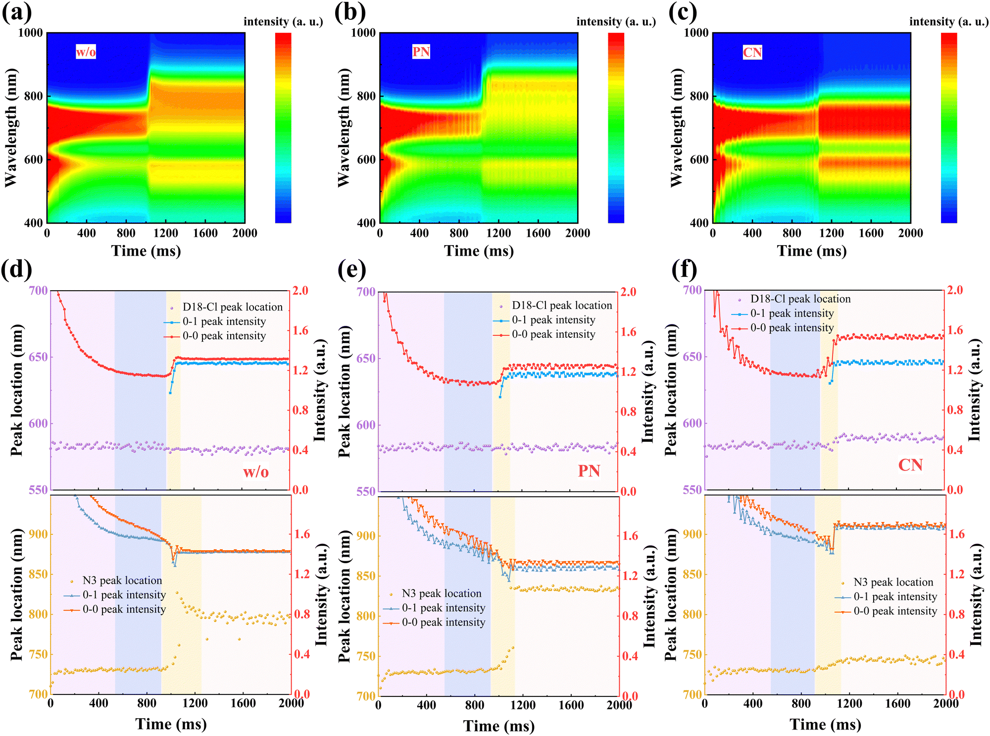 | ||
| Fig. 3 Time-dependent contour maps of in situ UV-Vis absorption spectra of the D18-Cl:N3 samples processed (a) without any additives (b) with 0.5 vol% PN and (c) with 0.5 vol% CN. Time evolution of the peak location and intensity of the donor and acceptor in the D18-Cl:N3 samples processed (d) without any additives (e) with 0.5 vol% PN and (f) with 0.5 vol% CN. | ||
In order to unveil the interactions between the additives and active materials, the Hansen solubility parameters (δ) of D18-Cl, N3, PN and CN were reviewed and are listed in Table S3 (ESI†).39–41 The solvent–molecular interaction parameters (χ) were calculated according to Flory–Huggins theory, and the results are as follows: χPN-D18-Cl = 1.04, χPN-N3 = 0.75, χCN-D18-Cl = 0.51, and χCN-N3 = 0.42. It is found that both PN and CN exhibit stronger interaction with the acceptor N3 than the donor D18-Cl, which is attributed to their π-conjugated structures that could enhance the van der Waals interactions with the end groups of NFAs.42 These interactions facilitate the insertion of additive molecules between adjacent acceptor tails and thereby create an additional space for relaxation and the subsequent ordered packing of NFA molecules. As a result, a reduced intermolecular π-stacking distance is obtained in the PN-treated D18-N3 films while the substantial steric hindrance associated with PN manipulates the dominant J-stacking arrangement. With regards to the CN additive, the lowest χCN-N3 suggests its good solubility for N3, and the high boiling point of CN is conducive for the H-aggregation of N3 molecules because slower evaporation facilitates molecular reorganization into their thermodynamically stable state in the film formation process.
The molecular aggregation of NFAs are potentially effective in promoting charge transport in the active layers and thereby improving the device performance, especially for thick OSCs. Therefore, to examine the impact of different aggregation behaviours enabled by PN and CN on the photovoltaic performance, we fabricated thin and thick OSCs using the conventional architecture of ITO/PEDOT:PSS/D18-Cl:N3/PFN-Br/Al with an active layer thickness of 120 nm and 300 nm, respectively. The representative current density–voltage (J–V) characteristics under 100 mW cm−2 AM 1.5G illumination and EQE curves are shown in Fig. 4, and the corresponding device parameters are summarized in Table 1. In the case of OSCs based on a 120 nm-thick active layer without additive, a moderate power conversion efficiency (PCE) of 16.15% was achieved with a VOC of 0.858 V, JSC of 25.91 mA cm−2, and FF of 73.26%. Upon the addition of 0.5 vol% PN, the PCE of the resultant device was enhanced to 18.02%, accompanied by a notably high JSC of 27.68 mA cm−2, VOC of 0.855 V and FF of 76.42%. For comparison, the OSCs processed with 0.5 vol% CN only yield a maximum PCE of 16.08% with a VOC of 0.860 V, JSC of 24.86 mA cm−2 and FF of 75.24%. The calculated JSC values from the EQE are in good agreement with the values achieved from the J–V measurements with a 5% mismatch. These results indicate that the J-aggregation of acceptors contributes to boosted JSC while H-aggregation helps to enhance the VOC values, consistent with the results reported.43
 | ||
| Fig. 4 (a) and (c) Illuminated J–V curves and (b) and (d) EQE spectra of the OSCs based on 120 nm or 300 nm-thick active layers with different additives (0.5 vol%). | ||
| Thickness (nm) | V OC (V) | J SC (mA cm−2) | J cal (mA cm−2) | FF (%) | PCEa(%) | |
|---|---|---|---|---|---|---|
| a The average PCE in the brackets was calculated from 10 devices. | ||||||
| Control | 120 | 0.858 (0.857 ± 0.006) | 25.91 (25.76 ± 0.44) | 25.44 | 72.98 (73.35 ± 1.01) | 16.22 (16.19 ± 0.47) |
| PN | 120 | 0.855 (0.844 ± 0.011) | 27.68 (26.90 ± 0.88) | 26.31 | 76.13 (75.87 ± 1.10) | 18.02 (17.70 ± 0.35) |
| CN | 120 | 0.860 (0.861 ± 0.003) | 24.86 (24.66 ± 0.21) | 24.32 | 75.24 (73.95 ± 1.37) | 16.08 (15.58 ± 0.52) |
| Control | 300 | 0.836 (0.839 ± 0.004) | 26.46 (26.65 ± 0.49) | 25.46 | 64.35 (63.98 ± 1.79) | 14.23 (14.36 ± 0.68) |
| PN | 300 | 0.827 (0.830 ± 0.010) | 27.69 (27.77 ± 0.93) | 26.49 | 71.98 (71.23 ± 0.75) | 16.48 (16.38 ± 0.41) |
| CN | 300 | 0.851 (0.846 ± 0.006) | 25.32 (24.99 ± 0.57) | 24.78 | 66.57 (66.07 ± 1.88) | 14.34 (14.12 ± 0.71) |
In addition, the OSCs with varied volume fraction of PN from 0.25% to 2.0% show relatively high PCEs exceeding 16.02%, as shown in Fig. S9 (ESI†), indicating an outstanding additive concentration tolerance. More importantly, the PN-incorporated OSCs display superior thickness tolerance from 120 nm to 350 nm compared to the control and CN-treated devices, as illustrated in Fig. S10 (ESI†). When the active layer thickness is increased to about 300 nm, the PCE of the PN-treated device is about 16.48%, along with a VOC of 0.827 V, high JSC of 27.69 mA cm−2 and FF of 71.98%, surpassing 14.23% and 14.34% for the control and CN-treated OSCs with the same active layer thickness, respectively. Both PN and CN additives can effectively improve the FF values while PN exhibits a more significant influence in thick OSCs, which is attributed to the more ordered molecular packing in the blend films. Moreover, the PN-treated device demonstrates remarkably increased JSC, mainly due to the broadened absorption spectra aroused by the enhanced J-aggregation of the N3 molecules. Conversely, the VOC of the PN-treated OSCs is decreased with regard to the CN-treated OSCs, which could probably be attributed to the dominant J-aggregation of N3 molecules.43,44 The synergistic improvement in the JSC and FF values enables the outstanding performance of the PN-treated thick OSCs.
The charge transport and extraction were investigated to elucidate the superior performance of OSCs processed with PN, especially for thick OSCs. The electron (μe) and hole mobility (μh) were measured via the space-charge limited current method, as presented in Table 2 and Fig. S11 in the ESI.† The μe and μh measured from the 120 nm PN-incorporated D18-Cl:N3 film were 1.67 × 10⁻³ and 1.35 × 10⁻³ cm2 V−1 s−1, respectively, significantly outperforming the control and CN-incorporated ones. In the case of the 300-nm-thick active layers, the μh and μe were calculated to be 0.83 × 10⁻³ and 0.87 × 10⁻³ cm2 V−1 s−1 for the control blend, 1.21 × 10⁻³ and 1.36 × 10⁻³ cm2 V−1 s−1 for the PN-treated blend, and 1.07 × 10⁻³ and 1.00 × 10⁻³ cm2 V−1 s−1 for the CN-treated blend, respectively. Obviously, both PN and CN additive could promote charge transport in the D18-Cl:N3 blend films regardless of their thickness due to improved molecular aggregation and crystallization. Compared to the CN additive, the PN-treated D18-Cl:N3 film demonstrates more pronounced enhancement of charge mobilities, contributing to higher JSC and FF values in the resultant OSCs. The photocurrent density (Jph) as a function of the effective voltage (Veff) for these OSCs is plotted in Fig. 5. For all the devices, Jph increases sharply with Veff in the low effective voltage region and reaches saturation current (Jsat) at Veff ≥ 3.0 V. The exciton dissociation (ηdiss) and charge collection efficiency (ηcoll) given in Table S4 (ESI†) were estimated from Jph/Jsat under short-circuit conditions and at the maximum power point, respectively.45 It is noted that all the devices show nearly identical exciton dissociation efficiency, which is attributed to the suitable phase separation in the D18-Cl:N3 active layers. In the case of thin OSCs, the charge collection efficiency is slightly enhanced from 86.12% for the control device to 87.12% and 87.60% for the CN- and PN-incorporated devices, respectively. The PN-treated thick OSCs still show a ηcoll of 87.30%, much higher than 80.56% and 84.79% for the control and CN-treated thick OSCs, respectively. These results indicate that the PN additive effectively enhances the charge transport and extraction behaviours, especially in the thick D18-Cl:N3 blend layer, thereby improving the photovoltaic performance of the corresponding thick OSCs.
| Thickness (nm) | μ h × 10−3 (cm2 V−1 s−1) | μ e × 10−3 (cm2 V−1 s−1) | μ h/μe | |
|---|---|---|---|---|
| D18-Cl:N3 | 120 | 1.02 | 1.25 | 1.22 |
| D18-Cl:N3-PN | 120 | 1.35 | 1.67 | 1.24 |
| D18-Cl:N3-CN | 120 | 1.14 | 1.44 | 1.26 |
| D18-Cl:N3 | 300 | 0.83 | 0.87 | 1.04 |
| D18-Cl:N3-PN | 300 | 1.21 | 1.36 | 1.12 |
| D18-Cl:N3-CN | 300 | 1.07 | 1.00 | 0.93 |
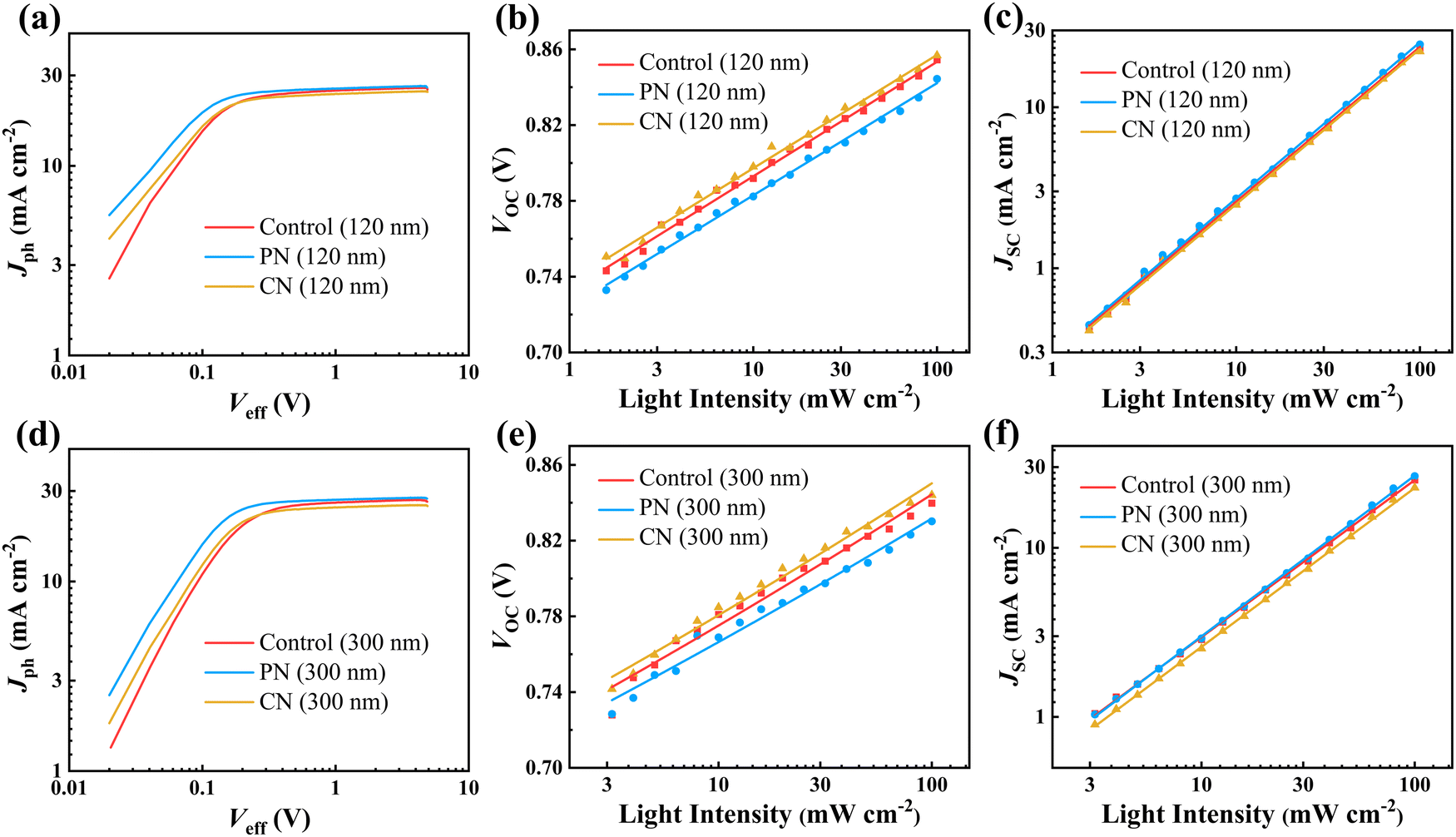 | ||
| Fig. 5 (a)–(c) Jph–Veff curves and the dependence of VOC and JSC on the light intensity of the 120-nm-thick D18-Cl:N3 OSCs. (d)–(f) Jph–Veff curves and the dependence of VOC and JSC on the light intensity of the 300 nm-thick D18-Cl:N3 OSCs. | ||
The dependence of VOC and JSC on illuminated light intensity (Plight) was measured to estimate the charge recombination status in thin and thick OSCs. The relationship between JSC and Plight can be described as JSC ∝ (Plight)α, where α is the power-law exponent representing the extent of bimolecular recombination.46 As displayed in Fig. 5, the extracted α values for the control, PN- and CN-incorporated thin OSCs were 0.96, 0.97, and 0.96, respectively. In case of the 300 nm-thick OSCs, the PN-treated device still exhibits the highest α value of 0.95 among the three kinds of devices. The dependence of VOC on the natural logarithm of Plight gives a slope of nkT/q, where k is the Boltzmann constant, T is the temperature, and q is the elementary charge.46 Alternatively, when monomolecular or trap-assisted recombination are involved, a strong dependence of VOC on the light intensity with a slope close to 2kT/q will be observed. The OSCs with 120-nm-thick active layers exhibit similar slopes of 1.01–1.03 kT/q, indicating negligible trap-assisted recombination. However, when the active layer thickness is increased to 300 nm, the fitted slopes of the control and CN-incorporated devices are 1.15 and 1.16 kT/q, respectively, much higher than 1.09 kT/q for the CN-incorporated device. The suppressed trap-assisted and bimolecular recombination enabled by the PN additive contributes to a remarkable improvement in the photovoltaic performance of thick OSCs.
Transient absorption (TA) spectroscopy was employed to further assess the charge generation in D18-Cl:N3 blends processed with different additives. The hole transfer process was firstly investigated by selectively exciting the acceptor N3 at a pump wavelength of 800 nm. The 2D color plots of the TA spectra for the neat films and D18-Cl:N3 blends pumped at 800 nm are shown in Fig. S12 and S17 (ESI†), and the TA spectra recorded at different time delays of the D18-Cl:N3 blends processed without and with the additives are depicted in Fig. S13 (ESI†) and Fig. 6(a), (b), respectively. Since D18-Cl cannot be pumped at 800 nm, the peak signal at 840 nm is ascribed to the ground state bleach (GSB) of N3 while the peak signal at 600 nm is assigned to the GSB of D18-Cl caused by the hole transfer from N3 to D18-Cl. Additionally, the excited-state absorption (ESA) signal for the local excited state of N3 is located at 930 nm, and a characteristic ESA signal after 1320 nm appeared upon optical excitation corresponding to an intermolecular delocalized excitation state due to the closely-packed N3 molecules. For the D18-Cl:N3 films, the fast decay of the N3 GSB signal after photoexcitation and a D18-Cl bleach signal that emerged within tens of picoseconds indicate the hole transfer process from N3 to the polymer D18-Cl.39,47Fig. 6(c) shows the faster GSB increase of D18-Cl in the PN-treated D18-Cl:N3 blend, implying more efficient hole transfer between D18-Cl and N3. We retrieved the kinetic traces of three D18-Cl:N3 blends at 600 nm in Fig. 6(c) and Table S4 (ESI†) through bi-exponential function fitting, where τ1 represents the ultrafast interfacial hole transfer process and τ2 is the diffusion of excitons in the acceptor phase toward the interfaces.7,48 The PN-treated D18-Cl:N3 film shows a τ1 of 0.54 ps and a τ2 of 5.53 ps. It is noted that the τ2 of the PN-treated D18-Cl:N3 film is shorter than 5.78 ps for the CN-incorporated blend film and 7.00 ps for the control blend film, manifesting faster exciton diffusion in the PN-treated films due to the improved molecular aggregation of N3. The almost same τ1 values in the different D18-Cl:N3 blend films might be attributed to their dominant face-on orientation of the donors and acceptors, which promote rapid hole transfer at the D/A interfaces. The investigation then focused on the photophysical process occurring in various D18-Cl:N3 blend films under photoexcitation at 420 nm, at which the polymer D18-Cl is excited. As seen in Fig. S14 (ESI†), the neat D18-Cl film exhibits a GSB peak at ∼600 nm and an ESA peak at 1200 nm instantly after photoexcitation. Due to the spectral overlap between D18-Cl photoluminescence and N3 absorption, as depicted in Fig. S16 (ESI†), it is predicted that a Förster resonance energy transfer (FRET) process may occur from the polymer D18-Cl to the acceptor N3. The 2D color plots of the TA spectra for the D18-Cl:N3 blends pumped at 420 nm are shown in Fig. S17 (ESI†), and the TA spectra recorded at different time delays are depicted in Fig. S15 (ESI†) and Fig. 6(d), (e), respectively. It is seen that the GSB of D18-Cl rapidly decays within the initial few hundred femtoseconds and then slowly increases within the ensuing timeframe of 1–50 ps. This phenomenon confirms that in addition to direct electron transfer, the FRET process also contributes to the charge generation in the D18-Cl:N3-based OSCs.49,50 Notably, the GSB signal of D18-Cl in the PN-treated D18-Cl:N3 films experiences a more pronounced resurgence, followed by a faster decay after 100 ps, indicating that the PN additive accelerates the FRET process from the photoexcited D18-Cl to N3 as well as the subsequent reverse hole transfer process from N3 to D18-Cl. The efficient hole transfer and enhanced FRET process facilitate charge generation and result in superior photovoltaic performance in PN-treated D18-Cl:N3 OSCs.
 | ||
| Fig. 6 (a) and (b) The line-cuts of fs-TA spectroscopy with pump at 800 nm at an indicated delay time of the PN- and CN-treated D18-Cl:N3 films. (c) The GSB kinetics of D18-Cl in different D18-Cl:N3 films excited at 800 nm. (d) and (e) The line-cuts of fs-TAS with pump at 420 nm at an indicated delay time of the PN- and CN-treated D18-Cl:N3 films. (f) The GSB kinetics of D18-Cl in different D18-Cl:N3 films excited at 420 nm. | ||
Conclusion
In summary, we manipulated the molecular aggregation behaviour of non-fullerene acceptors via a facile additive strategy to enhance the photovoltaic performance of the OSCs based on thick active layers. Two additives of PN and CN with different substituent steric hindrances were used in the bulk heterojunction D18-Cl:N3 active layer. It reveals that PN enables dominant J-aggregation of the acceptor N3 since the large phenyl substituents disturb the face-to-face π-stacking of adjacent N3 molecules. However, CN may enhance the H-aggregation of N3 acceptors during the film formation process due to its high boiling point and strong interaction with N3. Incorporation with PN or CN in the D18-Cl:N3 blend enhances molecular aggregations, leading to high charge mobilities that are crucial to thick OSCs. Moreover, the PN-treated D18-Cl:N3 active layer exhibits significantly red-shifted and broadened absorption spectra, which is beneficial for efficient light harvesting. The PN additive allows the OSCs based on 300-nm-thick D18-Cl:N3 active layer to achieve an efficiency of 16.48%, much higher than 14.23% of the corresponding devices without additive and 14.34% of the devices with the CN additive. This work provides an approach to regulate the molecular aggregation of non-fullerene acceptors towards high-performance thick OSCs.Experimental
Materials
PEDOT:PSS (Clevios PVP AI 4083) was purchased from Heraeus Materials Technology Germany. D18-Cl and N3 used in this work were obtained from Yirou Photovoltaic Technology Co. Ltd. PFN-Br was obtained from Solarmer Material Inc. Chloroform (CF) was purchased from Xilong Scientific Co. Ltd. 1-Phenylnaphthalene (PN) was from Alfa Aesar Inc., and 1-chloronaphthalene (CN) was from TCI Shanghai. All the materials and solvents were used as received without further purification.Device fabrication
The OSCs were fabricated with a conventional architecture of the ITO/PEDOT:PSS/active layer/PFN-Br/Al. The ITO glass substrates with a sheet resistance of 15 Ω square−1 were subjected to ultrasonic cleaning sequentially with detergent, deionized water, acetone, and isopropanol for 15 min of each step. The cleaned ITO glasses were then treated with UV-Ozone for 25 min before use. The hole transport layer of PEDOT:PSS (∼25 nm) was spin-coated on ITO glass substrate and annealed at 140 °C for 20 min in an oven. Then, the samples were moved into a glove box to spin-coat the active layer and the electron transport layer of PFN-Br. For the thin-film devices, the D18-Cl![[thin space (1/6-em)]](https://www.rsc.org/images/entities/char_2009.gif) :N3 blend solution in CF (1:1.6 in weight) was stirred at 60 °C for 30 min. CN or PN with a volume fraction of 0.5% was added and stirred for 30 min before spin-coating. In the preparation of the 300-nm-thick active layer films, a D18-Cl:N3 (1:1.6) solution with a concentration of 22.1 mg mL−1 was used. The solution was heated to 50 °C and spin-coated at 1800 rpm. The 120-nm-thick active layer films were spin-coated from a D18-Cl:N3 (1:1.6) solution with the total concentration of 15.6 mg mL−1 at a higher rotational speed of 3000 rpm. The concentrations and spin-coating speeds used for other active layers are detailed below. For the 150 nm-thick active layer films, a concentration of 15.6 mg mL−1 was employed and the rotational speed was 2200 rpm. The 200-nm-thick active layer films were prepared at a D18-Cl:N3 concentration of 18.2 mg mL−1 and a rotational speed of 2200 rpm. The 250-nm-thick films were produced with the same concentration of 18.2 mg mL−1 at a rotational speed of 1500 rpm. After spin-coating the D18-Cl:N3 film, the samples were thermally annealed at 90 °C for 3 min. Subsequently, the PFN-Br solution in menthol (0.5 mg mL−1) was spin-coated at 3000 rpm for 30 s. Finally, the Al cathode was thermally deposited with a shadow mask in a vacuum chamber. The active area of the cell was ca. 8 mm2.
:N3 blend solution in CF (1:1.6 in weight) was stirred at 60 °C for 30 min. CN or PN with a volume fraction of 0.5% was added and stirred for 30 min before spin-coating. In the preparation of the 300-nm-thick active layer films, a D18-Cl:N3 (1:1.6) solution with a concentration of 22.1 mg mL−1 was used. The solution was heated to 50 °C and spin-coated at 1800 rpm. The 120-nm-thick active layer films were spin-coated from a D18-Cl:N3 (1:1.6) solution with the total concentration of 15.6 mg mL−1 at a higher rotational speed of 3000 rpm. The concentrations and spin-coating speeds used for other active layers are detailed below. For the 150 nm-thick active layer films, a concentration of 15.6 mg mL−1 was employed and the rotational speed was 2200 rpm. The 200-nm-thick active layer films were prepared at a D18-Cl:N3 concentration of 18.2 mg mL−1 and a rotational speed of 2200 rpm. The 250-nm-thick films were produced with the same concentration of 18.2 mg mL−1 at a rotational speed of 1500 rpm. After spin-coating the D18-Cl:N3 film, the samples were thermally annealed at 90 °C for 3 min. Subsequently, the PFN-Br solution in menthol (0.5 mg mL−1) was spin-coated at 3000 rpm for 30 s. Finally, the Al cathode was thermally deposited with a shadow mask in a vacuum chamber. The active area of the cell was ca. 8 mm2.
Measurement and characterization
The UV-Vis absorption spectra were recorded using a UV-Vis Ocean Optics spectrophotometer. The AFM measurement was performed with a Bruker Dimension ICON AFM in the peak force mode. The thickness of the active layer was measured by a KLA Tencor P-7 surface profiler. TA spectra experiments were performed using a femtosecond pump–probe system. Illuminated current density–voltage (J–V) curves of the OSCs were recorded with a Keithley 2400 source meter under illumination of 100 mW cm−2 AM 1.5 G simulated solar light. The EQE of the devices was measured on an Enlitech QE-R spectral response measurement system.Data availability
The authors declare that all data supporting the results reported in this study are available within the paper and the ESI.† Additional data used for the study are available from the corresponding author upon reasonable request.Conflicts of interest
There are no conflicts to declare.Acknowledgements
The authors acknowledge the financial support from the Science and Technology Development Program of Jilin Province (20230101131JC), the National Natural Science Foundation of China (no. 52273200, 22135007 and 22361132545), and the National Key Basic Research and Development Program of China (2019YFA0705900) of the Chinese Ministry of Science and Technology.References
- Y. Wang, J. Yu, R. Zhang, J. Yuan, S. Hultmark, C. E. Johnson, N. P. Gallop, B. Siegmund, D. Qian, H. Zhang, Y. Zou, M. Kemerink, A. A. Bakulin, C. Müller, K. Vandewal, X. K. Chen and F. Gao, Nat. Energy, 2023, 8, 978–988 CrossRef.
- H. Liu, Y. Li, J. Wu, Y. Fu, H. Tang, X. Yi and Z. Xie, J. Mater. Chem. C, 2021, 9, 9914–9921 RSC.
- Z. Liu, Y. Fu, J. Wu, X. Yi, M. Zhao, M. Huang, J. Liu and Z. Xie, Adv. Funct. Mater., 2024, 34, 2401558 CrossRef.
- P. Cheng, G. Li, X. Zhan and Y. Yang, Nat. Photonics, 2018, 12, 131–142 CrossRef CAS.
- F. Sun, X. Zheng, T. Hu, J. Wu, M. Wan, Y. Xiao, T. Cong, Y. Li, B. Xiao, J. Shan, E. Wang, X. Wang and R. Yang, Energy Environ. Sci., 2024, 17, 1916–1930 RSC.
- J. Fu, P. W. K. Fong, H. Liu, C. S. Huang, X. Lu, S. Lu, M. Abdelsamie, T. Kodalle, C. M. Sutter Fella, Y. Yang and G. Li, Nat. Commun., 2023, 14, 1760 CrossRef CAS PubMed.
- J. Wang, Y. Wang, P. Bi, Z. Chen, J. Qiao, J. Li, W. Wang, Z. Zheng, S. Zhang, X. Hao and J. Hou, Adv. Mater., 2023, 35, 2301583 CrossRef CAS.
- L. Kong, Z. Zhang, N. Zhao, Z. Cai, J. Zhang, M. Luo, X. Wang, M. Chen, W. Zhang, L. Zhang, Z. Wei and J. Chen, Adv. Energy Mater., 2023, 13, 2300763 CrossRef CAS.
- Z. Chen, H. Yao, J. Wang, J. Zhang, T. Zhang, Z. Li, J. Qiao, S. Xiu, X. Hao and J. Hou, Energy Environ. Sci., 2023, 16, 2637–2645 RSC.
- X. Zheng, X. Wang, F. Sun, M. Wan, Z. Li, C. Xiao, T. Cong, T. Hu, Y. Liao and R. Yang, Chem. Eng. J., 2023, 475, 145520 CrossRef CAS.
- T. Xu, Z. Luo, R. Ma, Z. Chen, T. A. Dela Peña, H. Liu, Q. Wei, M. Li, C. E. Zhang, J. Wu, X. Lu, G. Li and C. Yang, Angew. Chem., Int. Ed., 2023, 62, e202304127 CrossRef CAS PubMed.
- C. Li, J. Zhou, J. Song, J. Xu, H. Zhang, X. Zhang, J. Guo, L. Zhu, D. Wei, G. Han, J. Min, Y. Zhang, Z. Xie, Y. Yi, H. Yan, F. Gao, F. Liu and Y. Sun, Nat. Energy, 2021, 6, 605–613 CrossRef CAS.
- L. Zhu, M. Zhang, J. Xu, C. Li, J. Yan, G. Zhou, W. Zhong, T. Hao, J. Song, X. Xue, Z. Zhou, R. Zeng, H. Zhu, C. C. Chen, R. C. I. MacKenzie, Y. Zou, J. Nelson, Y. Zhang, Y. Sun and F. Liu, Nat. Mater., 2022, 21, 656–663 CrossRef CAS PubMed.
- K. Chong, X. Xu, H. Meng, J. Xue, L. Yu, W. Ma and Q. Peng, Adv. Mater., 2022, 34, 2109516 CrossRef CAS PubMed.
- F. Zhao, C. Wang and X. Zhan, Adv. Energy Mater., 2018, 8, 1703147 CrossRef.
- Y. Chang, X. Zhu, K. Lu and Z. Wei, J. Mater. Chem. A, 2021, 9, 3125–3150 RSC.
- Y. Cai, Q. Li, G. Lu, H. S. Ryu, Y. Li, H. Jin, Z. Chen, Z. Tang, G. Lu, X. Hao, H. Y. Woo, C. Zhang and Y. Sun, Nat. Commun., 2022, 13, 2369 CrossRef CAS PubMed.
- T. Kirchartz, T. Agostinelli, M. Campoy Quiles, W. Gong and J. Nelson, J. Phys. Chem. Lett., 2012, 3, 3470–3475 CrossRef CAS PubMed.
- R. K. Gupta, R. Garai, M. Hossain, M. A. Afroz, D. Kalita and P. K. Iyer, J. Mater. Chem. C, 2021, 9, 8746–8775 RSC.
- H. R. Bai, Q. An, M. Jiang, H. S. Ryu, J. Yang, X. J. Zhou, H. F. Zhi, C. Yang, X. Li, H. Y. Woo and J. L. Wang, Adv. Funct. Mater., 2022, 32, 2200807 CrossRef CAS.
- L. Zhang, L. Hu, X. Wang, H. Mao, L. Zeng, L. Tan, X. Zhuang and Y. Chen, Adv. Funct. Mater., 2022, 32, 2202103 CrossRef CAS.
- Y. Zhu, X. Shen, H. Lai, M. Pu, Y. Zhu, X. Lai, S. Xiong and F. He, Nano Energy, 2023, 118, 108991 CrossRef CAS.
- X. Song, K. Zhang, R. Guo, K. Sun, Z. Zhou, S. Huang, L. Huber, M. Reus, J. Zhou, M. Schwartzkopf, S. V. Roth, W. Liu, Y. Liu, W. Zhu and P. Müller Buschbaum, Adv. Mater., 2022, 34, 2200907 CrossRef CAS.
- H. Hu, P. C. Y. Chow, G. Zhang, T. Ma, J. Liu, G. Yang and H. Yan, Acc. Chem. Res., 2017, 50, 2519–2528 CrossRef CAS.
- F. Zhao, D. He, C. Zou, Y. Li, K. Wang, J. Zhang, S. Yang, Y. Tu, C. Wang and Y. Lin, Adv. Mater., 2023, 35, 2210463 CrossRef CAS PubMed.
- X. Song, H. Xu, X. Jiang, S. Gao, X. Zhou, S. Xu, J. Li, J. Yu, W. Liu, W. Zhu and P. Müller Buschbaum, Energy Environ. Sci., 2023, 16, 3441–3452 RSC.
- H. Lai, Q. Zhao, Z. Chen, H. Chen, P. Chao, Y. Zhu, Y. Lang, N. Zhen, D. Mo, Y. Zhang and F. He, Joule, 2020, 4, 688–700 CrossRef CAS.
- W. Zhang, Y. Wu, R. Ma, H. Fan, X. Li, H. Yang, C. Cui and Y. Li, Angew. Chem., Int. Ed., 2023, 62, e202309713 CrossRef CAS PubMed.
- Q. Zhao, X. Yu, Z. Xie, J. Liu and Y. Han, ACS Appl. Energy Mater., 2018, 1, 6338–6344 CrossRef CAS.
- Q. Zhao, J. Liu, H. Wang, M. Li, K. Zhou, H. Yang and Y. Han, J. Mater. Chem. C, 2015, 3, 8183–8192 RSC.
- J. Kim, K. J. Baeg, D. Khim, D. T. James, J. S. Kim, B. Lim, J. M. Yun, H. G. Jeong, P. S. K. Amegadze, Y. Y. Noh and D. Y. Kim, Chem. Mater., 2013, 25, 1572–1583 CrossRef CAS.
- L. Ye, Y. Jing, X. Guo, H. Sun, S. Zhang, M. Zhang, L. Huo and J. Hou, J. Phys. Chem. C, 2013, 117, 14920–14928 CrossRef CAS.
- L. Xu, Y. Xiong, S. Li, W. Zhao, J. Zhang, C. Miao, Y. Zhang, T. Zhang, J. Wu, S. Zhang, Q. Peng, Z. Wang, L. Ye, J. Hou and J. Wang, Adv. Funct. Mater., 2024, 34, 2314178 CrossRef CAS.
- Y. Xie, H. S. Ryu, L. Han, Y. Cai, X. Duan, D. Wei, H. Y. Woo and Y. Sun, Sci. China: Chem., 2021, 64, 2161–2168 CrossRef CAS.
- S. Lilliu, T. Agostinelli, E. Pires, M. Hampton, J. Nelson and J. E. Macdonald, Macromolecules, 2011, 44, 2725–2734 CrossRef CAS.
- L. Chen, R. Ma, J. Yi, T. A. Dela Peña, H. Li, Q. Wei, C. Yan, J. Wu, M. Li, P. Cheng, H. Yan, G. Zhang and G. Li, Aggregate, 2024, 5, e455 CrossRef CAS.
- D. Luo, Z. Jiang, W. L. Tan, L. Zhang, L. Li, C. Shan, C. R. McNeill, P. Sonar, B. Xu and A. K. K. Kyaw, Adv. Energy Mater., 2023, 13, 2203402 CrossRef CAS.
- B. Lin, X. Zhou, H. Zhao, J. Yuan, K. Zhou, K. Chen, H. Wu, R. Guo, M. A. Scheel, A. Chumakov, S. V. Roth, Y. Mao, L. Wang, Z. Tang, P. Müller-Buschbaum and W. Ma, Energy Environ. Sci., 2020, 13, 2467–2479 RSC.
- X. He, C. C. S. Chan, X. Zou, S. Zhang, P. W. K. Fong, J. Kim, G. Li, X. Hu, W. Ma, K. S. Wong and W. C. H. Choy, Adv. Energy Mater., 2023, 13, 2203697 CrossRef CAS.
- L. Ye, Y. Xiong, M. Zhang, X. Guo, H. Guan, Y. Zou and H. Ade, Nano Energy, 2020, 77, 105310 CrossRef CAS.
- K. Yao, Y. X. Xu, X. Wang, F. Li and J. Yuan, RSC Adv., 2015, 5, 93689–93696 RSC.
- L. Mei, X. Xia, R. Sun, Y. Pan, J. Min, X. Lu, A. K. Y. Jen and X. K. Chen, Small, 2024, 20, 2305977 CrossRef CAS PubMed.
- Q. Zhao, H. Lai, H. Chen, H. Li and F. He, J. Mater. Chem. A, 2021, 9, 1119–1126 RSC.
- Q. Zhao and F. He, J. Energy Chem., 2024, 93, 174–192 CrossRef CAS.
- P. W. M. Blom, V. D. Mihailetchi, L. J. A. Koster and D. E. Markov, Adv. Mater., 2007, 19, 1551–1566 CrossRef CAS.
- S. He, Z. Shen, J. Yu, H. Guan, G. Lu, T. Xiao, S. Yang, Y. Zou and L. Bu, Adv. Mater. Interfaces, 2020, 7, 2000577 CrossRef CAS.
- R. Wang, C. Zhang, Q. Li, Z. Zhang, X. Wang and M. Xiao, J. Am. Chem. Soc., 2020, 142, 12751–12759 CrossRef CAS PubMed.
- Z. Chen, T. Wang, Z. Wen, P. Lu, W. Qin, H. Yin and X. T. Hao, ACS Energy Lett., 2021, 6, 3203–3211 CrossRef CAS.
- F. D. Eisner, M. Azzouzi, Z. Fei, X. Hou, T. D. Anthopoulos, T. J. S. Dennis, M. Heeney and J. Nelson, J. Am. Chem. Soc., 2019, 141, 6362–6374 Search PubMed.
- Z. Chen, C. He, P. Ran, X. Chen, Y. Zhang, C. Zhang, R. Lai, Y. Yang, H. Chen and H. Zhu, Energy Environ. Sci., 2023, 16, 3373–3380 RSC.
Footnote |
| † Electronic supplementary information (ESI) available. See DOI: https://doi.org/10.1039/d4tc03060e |
| This journal is © The Royal Society of Chemistry 2024 |