
Mixed valence that induces superior dielectric properties of CdCu3(Tb1/2Ta1/2)xTi4−xO12 ceramics†
Huan
Liu
a,
Xinyue
Yan
a,
Xinyue
He
a,
Zhanhui
Peng
 *a,
Di
Wu
a,
Pengfei
Liang
b,
Lingling
Wei
c,
Xiaolian
Chao
*a and
Zupei
Yang
*a
*a,
Di
Wu
a,
Pengfei
Liang
b,
Lingling
Wei
c,
Xiaolian
Chao
*a and
Zupei
Yang
*a
aKey Laboratory for Macromolecular Science of Shaanxi Province, Shaanxi Key Laboratory for Advanced Energy Devices, School of Materials Science and Engineering, Shaanxi Normal University, Xi’an 710119, Shaanxi, China. E-mail: pzh@snnu.edu.cn; chaoxl@snnu.edu.cn; yangzp@snnu.edu.cn
bSchool of Physics and Information Technology, Shaanxi Normal University, Xi’an 710119, Shaanxi, China
cSchool of Chemistry and Chemical Engineering, Shaanxi Normal University, Xi’an, 710119, Shaanxi, China
First published on 11th April 2025
Abstract
The considerable demand for energy and the accelerated growth of the microelectronics sector has prompted extensive research into dielectric materials with high dielectric constants for use in electronic storage devices. In this study, a conventional solid-phase method was used to enhance the dielectric properties of CdCu3Ti4O12 by co-doping Ti sites with Tb and Ta ions. Impressively, the CdCu3(Tb1/2Ta1/2)xTi4−xO12 ceramics exhibit superior dielectric properties with a dielectric constant (ε ∼ 3.21 × 10⁴) and a low loss tangent (tan![[thin space (1/6-em)]](https://www.rsc.org/images/entities/char_2009.gif) δ ∼ 0.020) at 1 kHz. In addition, the temperature dependent-coefficient of variation of its dielectric constant (Δε/ε25°C) is less than ±15% over the temperature range of −13 to 174 °C. The dielectric response is mainly due to intrinsic and extrinsic effects, and the inherent effects may be due to the formation of defect clusters (i.e.,
δ ∼ 0.020) at 1 kHz. In addition, the temperature dependent-coefficient of variation of its dielectric constant (Δε/ε25°C) is less than ±15% over the temperature range of −13 to 174 °C. The dielectric response is mainly due to intrinsic and extrinsic effects, and the inherent effects may be due to the formation of defect clusters (i.e.,  ,
, 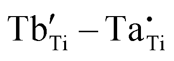 and
and  ). While the non-intrinsic effects are caused by the microstructure of the internal barrier layer capacitor, the impedance spectra show the presence of semiconductor grains as well as the huge resistance at the grain boundaries, where the heterogeneous structure causes an increase in grain boundary resistance. This study explores the dielectric response of a new type of giant dielectric ceramics and provides a new candidate for the fabrication of ceramic capacitors.
1. Introduction
Electric capacitors are prized for their high power density, elevated working voltage, and extended operational lifespan, making them highly effective in meeting the substantial demands of energy storage systems. They also offer promising applications in electronic systems that leverage pulse power technology. Giant dielectric materials exhibit an ultra-high dielectric constant (ε > 104), indicating a superior capacitance storage capacity compared to other dielectric materials of equivalent size and thickness. This remarkable characteristic aligns with the evolving trends in electronic component development, thus drawing considerable attention to research on giant dielectric materials.1–3 However, the critical parameters of giant dielectric materials hinder their wider application and development.4,5 For example, CaCu3Ti4O12-based (CCTO) materials suffer from high loss tangent (tanδ) and exhibit frequency/temperature instabilities of ε.6,7 To meet the changing demands of modern electronics development, it is crucial to optimize the performance and reliability of the materials.
Previous studies have reported that various elemental doping strategies have been employed to modify structure and tuned dielectric behavior of CCTO ceramics. For instance, doping with Zn,8 Zr/Nd9 and In/Ta10 has been reported to enhance dielectric properties of CCTO. Rare earth (RE) elements are known as “industrial vitamins” in the post-industrial era. The rare earth elements La,11 Eu,12 Dy,13 Yb,14 Tb,15 Y/Mg,16 Pr/Co17 and Gm/Sm18 are widely used in CCTO ceramics for dielectric modification. In the above compounds, The RE ions predominantly replace Ca site in the CCTO lattice, leading to the formation of Ca1−3x/2RExCu3Ti4O12 or Ca1−xRExCu3−yAyTi4O12 compounds. When RE ions are doped at the Ca site, ε tends to decrease while tanδ tends to increase. However, the doping of RE ions at the Ti site in CCTO has rarely been documented. Besides the improved dielectric characteristics, the dielectric mechanisms exhibited by CCTO ceramics have become a subject of significant interest. Typically, the dielectric behavior in giant dielectric materials is a result of both intrinsic and extrinsic contributions. Thomas et al.19 summarized ten mechanisms, while studies on grain boundary and first-principles calculations confirmed the external effects of CCTO.20,21 The internal barrier layer capacitance (IBLC) model connects inhomogeneous structure consisting of ceramics conductive grains and insulating grain boundaries to electrical performance.22 With its emphasis on microstructural inhomogeneities, this model is now broadly recognized as the leading plausible explanation for the giant dielectric response.
Research has revealed that introducing donor ions, such as Nd3+, into CCTO ceramics alongside valent dopants like Zr4+ effectively enhances grain boundary resistance and significantly improves dielectric properties.9 Furthermore, co-doping Ti4+ with covalent elements proves to be an efficient method for reducing the tanδ of CCTO ceramics while preserving a high ε. For example, co-doping CCTO ceramics with Al3+ and Nb5+ enhances the relative dielectric constant (ε ∼ 4.0 × 10⁴), while also leading to a reduction in dielectric loss (tanδ ∼ 0.050).23 In this study, the selected donor ion was the pentavalent dopant Ta5+ (r6 = 0.64 Å), which closely matches the ionic radius of the host Ti4+.24 Ta5+ has an extra layer of outer electrons, has a strong electron binding ability to make the electrons more localized, and is expected to completely displace the Ti4+ position. Meanwhile, Tb ions with distinct ionic radii (Tb3+: r6 = 0.92 Å and Tb4+: r6 = 0.76 Å) were chosen as covalent/equivalent dopants.25 The varying valence states and ionic radii of Tb ions were explored to assess their effect on the dielectric properties. Doping with the larger Tb3+ ions can induce the formation of defect clusters or oxygen vacancy-related defects ( ). The doping of CCTO-based materials with equivalent dopants has been observed to result in a lower concentration of
  , as evidenced by Sn4+ doped CCTO ceramics.26 Moreover, the equivalent doping of Tb4+ increases the grain-boundary resistance, and excessive doping may hinder the formation of
  . The expected result of embedding these dopants into the CCTO lattice is a systematic augmentation of the material's dielectric features.
The CdCu3Ti4O12 (CdCTO) ceramic structure is classified as a chalcogenide-like structure. Cd2+ (1.31 Å) and Ca2+ (1.34 Å) exhibit similar ionic radii when in 12-fold coordination. However, their initial dielectric properties of CdCTO and CCTO ceramics differ significantly. Subramanian et al.27 reported that the ε (∼409) of pristine CdCTO is relatively low, while the tanδ (∼0.093) is considerably high. Recently, through the enhancement of the preparation methods and the alteration of doping, we have successfully prepared dielectric ceramics with exceptional dielectric properties in our research team (ε > 2.0 × 10⁴, tanδ < 0.1).28–30 Based on the IBLC effect, grain boundary and grain resistance can be tuned by hetero/covalent element doping to enhance overall dielectric properties. Unfortunately, the co-doping of CdCTO with Tb3+/4+ and Ta5+ at Ti sites to improve dielectric properties has never been reported.
To improve the performance of CdCTO-based ceramics, we applied a conventional solid-phase method in this study. Tb3+/Tb4+ ions were introduced as acceptor/equivalent dopants, while Ta5+ acted as a donor dopant to optimize dielectric properties through inter-ion self-charge compensation and the improvement of grain boundary resistance. The results show that ε and low tanδ values remain stable over a specific range of frequency and temperature. Notably, the TT10 ceramics exhibited the best performance (ε ∼ 3.21 × 10⁴, tanδ ∼ 0.020 at 1 kHz). The microstructure and possible defect clusters within the ceramics have been comprehensively analyzed, providing a detailed discussion of the mechanisms underpinning the giant dielectric response.
2. Experimental
The synthesis of CdCu3(Tb1/2Ta1/2)xTi4−xO12 ceramics was carried out via the traditional solid-state reaction pathway, with x values specified as 0.01, 0.025, 0.05, 0.10, and 0.20. The samples can be abbreviated as TT01, TT025, TT05, TT10, and TT20, respectively. The raw materials utilized in the process included CdO (99%), CuO (99%), TiO2 (98%), Tb4O7 (99.99%), and Ta2O5 (99.99%). The materials underwent wet ball milling with agate balls in anhydrous ethanol, followed by drying at 80 °C in a thermostatic oven, subsequent milling, and pre-firing. Polyvinyl alcohol (PVA) at 5% by mass was added to the pre-fired powder for granulation and sieving. With a pressure of 6 MPa, the screened powder was compacted into pellets with a diameter of 11.5 mm and a thickness of approximately 1.0 mm. Subsequently, the sintering of the pellets was carried out at 1020 °C for 15 hours. After sintering, the samples were ground with emery and polished with a polishing compound, then ultrasonically cleaned. Subsequently, silver electrodes were applied using screen printing technique with silver paste. Finally, the ceramic samples were sintered in a chamber furnace at 840 °C for 30 minutes to ensure proper contact between the samples and electrodes for subsequent testing.To analyze the phase structure and microstructure of the CdCTO-based ceramics, an X-ray diffractometer (XRD, MiniFlex600, Rigaku) and a scanning electron microscope (SEM, SU3500, Hitachi) were employed. Raman spectral shifts were analyzed via laser Raman spectrometry (inVia Reflex, Renishaw, England). The field emission scanning electric microscopy (FE-SEM, SU8020, Hitachi) and energy dispersive spectrometer (EDS, X-MAX80, Horiba) systems were used in tandem to further assess the elemental distribution and chemical composition. The precision LCR meter (4294A, Agilent) was used to assess impedance spectra and the dielectric performance at room temperature. The temperature dependent of dielectric properties and impedance spectra were obtained using dielectric temperature spectroscopy measuring system (DMS2000, Balab). The analysis of the chemical valence states of elements in CdCTO-based ceramics was conducted using an X-ray photoelectron spectrometer (XPS, Kratos Analytical Ltd, AXIS ULTRA) and experimental data fitting was performed with Casa XPS software.
3. Results and discussion
The XRD patterns of CdCu3(Tb1/2Ta1/2)xTi4−xO12 ceramics are illustrated in Fig. 1(a). The presence of characteristic peaks in the XRD patterns of all samples matching those of CdCTO (PDF# 48-0208), which indicates the successful substitution of Tb and Ta into the lattice. Notably, only the primary CdCTO crystalline phase was observed, without the production of secondary phases usually found in similar compounds, such as CuO,31,32 Tb4O7 (PDF # 13-387), or Tb2Ti2O7 (PDF # 41-363).33 The solubility limit of Tb ions in CdCu3(Tb1/2Ta1/2)xTi4−xO12, as determined by experiments, exceeds x = 0.20. The chalcogenide-like material CCTO crystallizes in a body-centered cubic matrix containing 20 atoms, falling under the centrosymmetric Th (Im![[3 with combining macron]](https://www.rsc.org/images/entities/char_0033_0304.gif) ) space group. The Im crystallographic structure generates 24 Γ-point phonons, with eight identified as Raman-active modes.34,35 CdCTO exhibits weak Raman scattering, with only five of the eight modes being detectable, specifically at F1g ∼ 263 cm−1, E1g ∼ 322 cm−1, A1g ∼ 444 cm−1, A2g ∼ 510 cm−1 and F3g ∼ 576 cm−1. Among these five modes, the modes 444, 510 and 576 cm−1 are relatively intense, whereas 263 and 322 cm−1 are weaker. The F1g (∼263 cm−1), E1g (∼322 cm−1), A2g (∼510 cm−1), and A1g (∼444 cm−1) modes correspond to symmetric rotational vibrations of the [TiO6] octahedral structure. Meanwhile, F3g (∼576 cm−1) represents the asymmetric telescopic vibrational mode of Ti–O–Ti.34,36–38 The successful substitution of Ti lattice sites with Tb and Ta ions in CdCTO ceramics was confirmed by XRD and Raman spectroscopy analyses. Furthermore, neither a second phase was formed nor the solid solution limit was exceeded in the compounds, which further confirms the successful synthesis of a homogeneous solid solution of CdCu3(Tb1/2Ta1/2)xTi4−xO12.
) space group. The Im crystallographic structure generates 24 Γ-point phonons, with eight identified as Raman-active modes.34,35 CdCTO exhibits weak Raman scattering, with only five of the eight modes being detectable, specifically at F1g ∼ 263 cm−1, E1g ∼ 322 cm−1, A1g ∼ 444 cm−1, A2g ∼ 510 cm−1 and F3g ∼ 576 cm−1. Among these five modes, the modes 444, 510 and 576 cm−1 are relatively intense, whereas 263 and 322 cm−1 are weaker. The F1g (∼263 cm−1), E1g (∼322 cm−1), A2g (∼510 cm−1), and A1g (∼444 cm−1) modes correspond to symmetric rotational vibrations of the [TiO6] octahedral structure. Meanwhile, F3g (∼576 cm−1) represents the asymmetric telescopic vibrational mode of Ti–O–Ti.34,36–38 The successful substitution of Ti lattice sites with Tb and Ta ions in CdCTO ceramics was confirmed by XRD and Raman spectroscopy analyses. Furthermore, neither a second phase was formed nor the solid solution limit was exceeded in the compounds, which further confirms the successful synthesis of a homogeneous solid solution of CdCu3(Tb1/2Ta1/2)xTi4−xO12.
 | ||
| Fig. 1 (a) XRD patterns of CdCTO-based ceramics. (b) Raman patterns of CdCTO-based ceramics. | ||
Fig. 2(a)–(d) illustrates the hot corrosion microstructures of CdCu3(Tb0.5Ta0.5)xTi4−xO12 ceramics. These images reveal pronounced grain boundaries and excellent crystallinity in all the prepared ceramics, with the insets presenting the grain size distribution. As the Tb/Ta doping level increases to x = 0.10, the decrease in average grain size (ADS) shifting to 27.9 ± 0.5 μm, accompanied by a more homogeneous grain size distribution. The observed decrease in ADS may result from the solute drag phenomenon related to Ta ion and the inhibition of grain growth by Tb ion.35,39 In conclusion, increasing doping levels lead to a diminished grain size, and this microstructural evolution may influence their dielectric properties. The observed trend indicates a critical balance between doping levels and the resultant microstructure and electrical properties.
 | ||
| Fig. 2 SEM images of samples, and the inserts show the rain size distribution. (a) TT01, (b) TT025, (c) TT05, (d) TT10. | ||
Additionally, the electron dispersive spectroscopy displays the elemental distribution of thermally etched TT10 ceramic as illustrated in Fig. S1 (ESI†). The elements Tb and Ta exhibit nearly uniform diffusion into the CdCTO lattice. At the grain boundaries, Cu segregates to form a Cu-rich phase, The IBLC model identifies these Cu-rich phases as insulating grain boundaries and Cu-deficient phases as semiconductor grains.40–43 Dopant ions with larger ionic radii introduce lattice distortion, which promotes the development of a Cu-rich layer along the grain boundaries. This layer boosts grain boundary resistance, effectively reducing the low-frequency dielectric loss in the ceramics.41,44
To assess the influence of co-doped Tb/Ta ions on the dielectric properties of CdCTO-based ceramics, their frequency-dependent behavior was analyzed. The dielectric properties of TT01, TT025, TT05 and TT10 ceramics at room temperature and across a frequency range of 40–106 Hz are illustrated in Fig. 3(a). The tested samples all exhibit a broad dielectric plateau and demonstrate superior frequency stability. Fig. 3(c) compares the ε and tanδ of the ceramics, revealing that all samples display colossal ε > 2.10 × 10⁴ and low tanδ < 0.04 at 1 kHz. These findings confirm that the dielectric properties are largely independent of frequency. However, as shown in Fig. 3(b), when x exceeds 0.10, both the ε and tanδ deteriorate significantly. This degradation is attributed to the excessive doping, which increases interfacial layers within the ceramics. Consequently, the interfacial effects are notably influenced, leading to a corresponding deterioration in the dielectric properties.45
 | ||
| Fig. 3 (a) Frequency dependence of the dielectric performance for CdCTO-based ceramics, the inset shows the dielectric loss diagram at low frequencies. (b) Frequency dependence of the dielectric performance for TT20. (c) The dielectric constant and dielectric loss at 1 kHz. (d) Room temperature conductivity of CdCTO-based ceramics. | ||
Fig. 3(d) illustrates the link between AC conductivity (σ′) and frequency (f) of co-doped CdCTO-based at room temperature. Below f = 105 Hz, σ′ remains nearly constant, while a sharp increase is observed beyond f = 106 Hz. Notably, the conductivity of the ceramics increases gradually with doping in the high-frequency region, a trend closely related to the resistance of the semiconductor grains.35 Conversely, at low frequencies, all ceramic samples exhibit conductivity approaches zero, which is primarily attributable to the response of the insulating grain boundary resistance.
In order to reveal the inhomogeneity and relaxation mechanism of CdCu3(Tb1/2Ta1/2)xTi4−xO12 ceramics, impedance spectroscopy was utilized for a comprehensive analysis of their electrical response. Following the IBLC model, the impedance spectrum shows the inhomogeneity of grain boundary resistance (Rgb) and grain resistance (Rg).46 The values of Rgb and Rg were calculated using the ZSimp Win software, which utilized an equivalent circuit comprising two series-connected RC elements. The relationship between the impedance real (Z′) and impedance imaginary (Z′′) components of impedance is depicted in Fig. 4, along with the corresponding Rg and Rgb values for the ceramic sample at room temperature.47 In Fig. 4(b), large semicircular curve is visualized with respect to the insulating grain boundaries. while the non-zero intercepts at high frequencies indicate that semiconducting grains are present. Notably, the Rgb values ranging from approximately 9.21 × 10⁵ to 3.84 × 10⁶ Ω, are considerably higher than the Rg values, which span from 3.23 to 8.31 Ω. The disparity in impedance values suggests that grain boundary relaxation exerts a key factor influence in the dielectric behavior of ceramics.
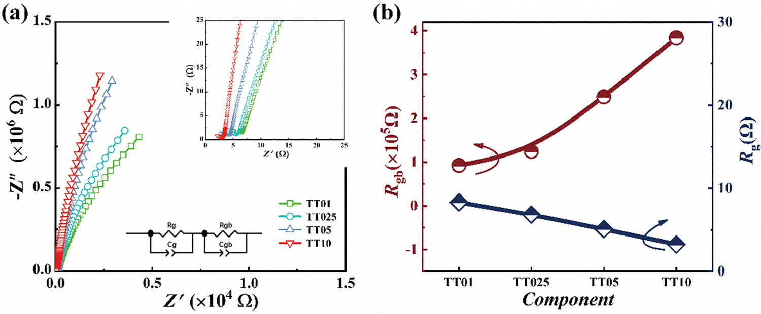 | ||
| Fig. 4 (a) The complex impedance at room temperature. (b) Rgb and Rg values of CdCTO-based ceramics. | ||
The temperature stability is a parameter that measures the ability of a dielectric material to be used in practical applications. Fig. 5 illustrates the temperature-dependent variation in the dielectric properties of TT01 and TT10, which was used to evaluate the thermal stability of the ceramic. It can be observed that the dielectric temperature stability of TT10 is optimal, with the dielectric constant remaining nearly constant from RT to 200 °C. As illustrated in Fig. 6(a) and (b), the dielectric temperature profile of the ceramics reveals two distinct relaxation peaks, denoted as A1 (−150 ∼ 0 °C) and A2 (0 ∼ 150 °C). These peaks are attributed to thermally activated Debye-like relaxation behavior.48,49 Generally, A1 relaxation close to room temperature is associated with inter-electron hopping (Ti4+–Ti3+).50 Conversely, the A2 relaxation observed at higher temperatures is linked to interfacial polarization.51 Notably, the amplitude of the A2 dielectric relaxation peak decreases significantly in the high-temperature region, especially in the case of optimal double doping. This reduction likely contributes to the enhanced temperature stability of the doped ceramics.
 | ||
| Fig. 5 Temperature dependent dielectric properties and temperature coefficients of dielectric constant for CdCTO-based ceramics. (a) TT01, (b) TT10. | ||
 | ||
| Fig. 6 TT10 ceramics at different temperatures from 100 to 390 °C. (a) Plot of real part (Z′) versus frequency. (b) Plot of imaginary part (−Z′′) versus frequency. | ||
Moreover, the temperature coefficient of dielectric constant (TCK), which is crucial for the practical implementation of ceramics and is calculated as:
 | (1) |
Here, CT represents the capacitance of ceramics at the tested temperature and C25°C is the capacitance at 25 °C.52 The TT10 ceramics exhibit a narrow temperature range in which the relative change in dielectric constant (Δε/ε25°C) does not exceed ±15%. It is noteworthy that the most thermally stable TT10 ceramics demonstrate a TCK variation of under ±15% throughout the temperature range from −13 to 174 °C. This performance aligns with the stringent requirements for Z8R capacitor applications (Δε/ε25°C ≤ ±15% from 10 to 150 °C). This characteristic forms the basis of their application in cutting-edge electronic components where consistent performance is critical.
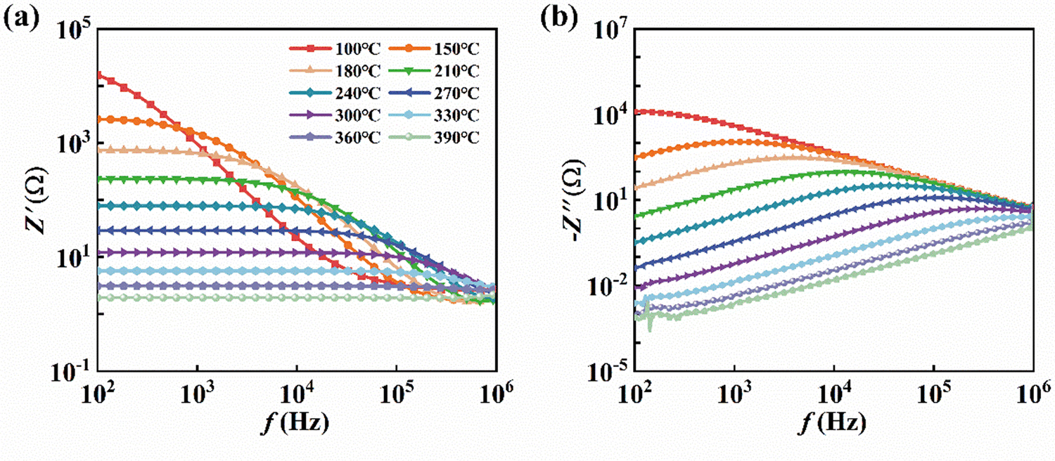
The analysis of Z′ and Z′′ impedance components as a function of frequency offers valuable understanding of the sample's relaxation behavior. Fig. 6 presents the plot of impedance against frequency for TT10 ceramics within a temperature range of 100 to 390 °C. Fig. 6(a) illustrates the impedance characteristics, where Z′ decreases as both frequency and temperature increase, suggesting enhanced alternating current conductivity. With increasing temperature, the impedance plateau observed at low frequencies extends into the high-frequency range and converges to a single curve. This behavior is attributed to diminished potential barrier and the subsequent release of space charge.53–55 Generally, the high-temperature, low-frequency impedance plateau in Z′ coexists with a Debye-like relaxation peak in Z′′.56 The corresponding Debye-like relaxation peak is visible in Fig. 7(b). The shift of the relaxation peak shifts toward higher frequencies with rising temperature indicates the occurrence of thermally activated relaxation behavior. In contrast, the low-frequency relaxation peak is mainly caused by the contribution of grain boundaries. Consequently, the impedance plot allows for the observation of both the grain boundary effects and grain contributions.
 | ||
| Fig. 7 Complex impedance of CdCTO-based ceramics at different temperature and the insert shows the relationship about lnσgb and 1000/T for CdCTO-based ceramics. (a) TT01, (b) TT025, (c) TT05, (d) TT10. | ||
Fig. 7 illustrates the complex impedance of ceramics is presented for temperature ranging from 100 to 270 °C. At higher temperatures, a complete Nyquist semicircular plot is evident. Charge carriers in giant dielectric materials are readily excited at high temperatures, which leads to their long-range migration.57 The equation provided can be used to calculate the value in question:
 | (2) |
 | (3) |
σgb) versus temperature (1000/T) is shown in the inset of Fig. 7 in conjunction with eqn (3). The sample exhibits grain boundary relaxation behavior, which can overcome a potential barrier energy of 0.71–0.83 eV. Generally, electron transfer is hindered in ceramics with high activation energy, which results in low losses.
As depicted in Fig. 8, the formation of defect clusters plays a critical role in the dielectric response of ceramics. In order to further investigate the origin of the giant dielectric constant mechanism, we conducted XPS analysis on the TT10 samples. Fig. 8(a) illustrates the distinct 2d peaks of Cd at 402.3 and 409.1 eV within the ceramic samples, with no additional valence transitions observed. In Fig. 8(b), the O 1s spectrum reveals a binding energy of 526.7 eV, typically associated with the Ti–O bond. The peak at 528.5 eV corresponds to 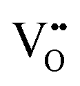 in the sample or to the hydroxyl group (OH) present on the sample's surface.59,60 Generally, Ta5+ functions as a donor by providing electrons to Ti4+, reducing it to Ti3+. Simultaneously, Tb3+ serves as an acceptor by substituting for Ti4+, resulting in the formation of charge-neutral
  to compensate for the introduction of trivalent ions. The formation process is described by in eqn (5) and (6):
 | (5) |
 | (6) |
 | ||
| Fig. 8 The XPS spectra of TT10 ceramics, (a) Cd, (b) O, (c) Cu, (d) Ta, (e) Tb, (f) Ti. | ||
The Cu in the ceramic samples exists in a mixed Cu+/Cu2+ valence state, as illustrated in Fig. 8(c). A prominent peak at approximately 931.0 eV corresponds to Cu2+, while a secondary set of peaks at a lower binding energy (∼928.2 eV) indicates the suggests of Cu+.61 During the high-temperature sintering process, electrical compensation for Cu+ occurs via the formation of oxygen vacancies.62 The two XPS peaks observed at 24.35 and 22.40 eV in Fig. 8(d) correspond to Ta 4f5/2 and 4f7/2, respectively. This suggests that the oxidation valence state of Ta is +5.58
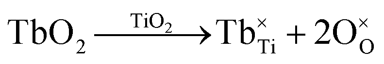
Fig. 8(e) displays the XPS spectrum of Tb 4d, indicating the existence of Tb3+/Tb4+ mixed valence states. The observed binding energies of about 153.3 eV and 150.1 eV provide evidence for the presence of mixed-valence Tb3+/Tb4+ states. As Tb4+ is an equivalent dopant, it is expected that Tb4+ substitutes Ti4+ in TiO2 without creating  .63 As assumed in the reaction according to eqn (7):
 | (7) |
The XPS spectra of the Ti element are presented in Fig. 8(f), where the binding energies of 460.90 and 455.05 eV correspond to the two characteristic orbital peaks of Ti 2p1/2 and 2p3/2, respectively, confirming the presence of Ti4+. Additionally, two smaller peaks at 459.25 and 455.75 eV are observed, further indicating the presence of Ti3+, with the introduction of Ta5+ providing free electrons to the system.64 As shown in eqn (8)–(9), Ti4+ is reduced to Ti3+ after gaining electrons:
 | (8) |
| Ti4+ + e− → Ti3+ | (9) |
In summary, Ta5+ and Tb3+/4+ ions occupy the Ti4+ sites, and the semiconducting grains of the ceramics arise from electron hopping between Ti4+ and Ti3+. The coupling effect between the defects restricts carrier transport and achieves lower losses, which is essential for understanding the mechanism of the dielectric properties.
4. Conclusion
In summary, the preparation of a novel low-loss CdCu3(Tb1/2Ta1/2)xTi4−xO12 ceramic is described, achieved through a conventional solid-phase method, and investigates the source of the giant dielectric mechanism. The TT10 ceramic exhibits remarkable dielectric properties, with ε ∼ 3.21 × 10⁴ and tanδ ∼ 0.020 at 1 kHz. Furthermore, across the temperature range of −13 to 174 °C, the variation of ε relative to its 25 °C value (Δε/ε25°C) remains within ±15%. The dielectric response mechanism of CdCu3(Tb1/2Ta1/2)xTi4−xO12 ceramics has also been investigated. Analyses of XPS and relaxation behavior reveal that the grain boundary resistance is enhanced by equipotent doping, while the optimization of dielectric properties attributed to the IBLC effect. Additionally, the defect structure may influence performance. It is evident that further investigations are needed to enhance the dielectric properties of CdCTO ceramics and to gain insight into the response mechanisms. This will facilitate the expansion of their applications in modern electronics, sensors and other fields.
Data availability
The data that support the findings of this study are available from the corresponding author and first author upon reasonable request.Conflicts of interest
The authors declare that they have no known competing financial interests or personal relationships that could have appeared to influence the work reported in this paper.Acknowledgements
This work was supported by the National Science Foundation of China (NSFC) (grant no. 52202143, 52272119 and 51872177). The authors would also like to thank the Young Talent Fund of University Association for Science and Technology in Shaanxi, China (20230415), the Fundamental Research Funds for the Central Universities (Grant No. GK202401009), the Excellent Graduate Training Program of Shaanxi Normal University (No. LHRCCX23223) and the Fundamental Innovation Project in School of Materials Science and Engineering (SNNU).References
- Z. Lv, T. Lu, Z. Liu, T. Hu, Z. Hong, S. Guo, Z. Xu, Y. Song, Y. Chen, X. Zhao, Z. Lin, D. Yu, Y. Liu and G. Wang, NaNbO3-Based Multilayer Ceramic Capacitors with Ultrahigh Energy Storage Performance, Adv. Energy Mater., 2024, 14, 2304291 CrossRef CAS.
- Z. M. Dang, J. K. Yuan, S. H. Yao and R. J. Liao, Flexible nanodielectric materials with high permittivity for power energy storage, Adv. Mater., 2013, 25, 6334–6365 CrossRef CAS PubMed.
- X. Hao, A review on the dielectric materials for high energy-storage application, J. Adv. Dielectr., 2013, 03, 1330001 CrossRef.
- W. Hao, P. Xu, P. Han and M. Wang, Optimize the dielectric properties of CaCu3Ti4O12 ceramics by adjusting the conductivities of grains and grain boundaries, J. Eur. Ceram. Soc., 2023, 43, 986–992 CrossRef CAS.
- T. Yang and J. Liang, High breakdown electric field in (Ta1−xPrx)0.03Ti0.97O2 colossal permittivity ceramics through defect chemistry optimization, J. Alloys Compd., 2022, 929, 167323 CrossRef CAS.
- R. Wu, Z. Fu, Y. Liu, Y. Wei, H. Sun, A. Chang and B. Zhang, Widening the temperature range and improving the linearity of CaCu3Ti4O12 ceramics for high-temperature NTC thermistor application through entropy engineering strategy, J. Alloys Compd., 2024, 973, 172908 CrossRef CAS.
- P. Mao, C. Zeng, Y. Guo, G. Lu, Q. Yan, Z. Liu, B. Xie, Y. Zhao, K. Guo and L. Zhang, Tuning electrical heterogeneity in CaCu3Ti4O12–ZnO ceramics for high dielectric and nonlinear properties, Mater. Res. Bull., 2023, 164, 112276 CrossRef CAS.
- L. Ni and X. M. Chen, Enhancement of giant dielectric response in CaCu3Ti4O12 ceramics by Zn substitution, J. Am. Ceram. Soc., 2010, 93, 184–189 CrossRef CAS.
- S. Rani, N. Ahlawat, K. M. Sangwan, S. Rani, R. Punia and J. Malik, Structural investigation and giant dielectric response of CaCu3Ti4O12 ceramic by Nd/Zr co-doping for energy storage applications, J. Mater., 2018, 29, 10825–10833 CAS.
- J. Boonlakhorn, P. Srepusharawoot and P. Thongbai, Distinct roles between complex defect clusters and insulating grain boundary on dielectric loss behaviors of (In3+/Ta5+) co-doped CaCu3Ti4O12 ceramics, Res. Phys., 2020, 16, 102886 Search PubMed.
- S. Vangchangyia, T. Yamwong, E. Swatsitang, P. Thongbai and S. Maensiri, Selectivity of doping ions to effectively improve dielectric and non-ohmic properties of CaCu3Ti4O12 ceramics, Ceram. Int., 2013, 39, 8133–8139 CrossRef CAS.
- G. Evangeline T, R. Annamalai A and P. Ctibor, Effect of Europium Addition on the Microstructure and Dielectric Properties of CCTO Ceramic Prepared Using Conventional and Microwave Sintering, Molecules, 2023, 28, 1649 CrossRef CAS PubMed.
- R. Kashyap, R. K. Mishra, O. P. Thakur and R. P. Tandon, Structural, dielectric properties and electrical conduction behaviour of Dy substituted CaCu3Ti4O12 ceramics, Ceram. Int., 2012, 38, 6807–6813 CrossRef CAS.
- K. He, Y. Luo, R. Yu, J. Qi, X. Sun, Y. Yang, H. Xu, J. Ma and D. Xu, Influence of Yb2O3 on electrical and microstructural characteristics of CaCu3Ti4O12 ceramics, Mater. Res. Bull., 2015, 69, 98–103 CrossRef CAS.
- P. Thongbai, J. Boonlakhorn, B. Putasaeng, T. Yamwong and S. Maensiri, Extremely enhanced nonlinear current-voltage properties of Tb-Doped CaCu3Ti4O12 ceramics, J. Am. Ceram. Soc., 2013, 96, 379–381 CrossRef CAS.
- J. Boonlakhorn, B. Putasaeng, P. Kidkhunthod and P. Thongbai, Improved dielectric properties of (Y + Mg) co-doped CaCu3Ti4O12 ceramics by controlling geometric and intrinsic properties of grain boundaries, Mater. Des., 2016, 92, 494–498 CrossRef CAS.
- J. Mohammed, T. T. Carol, H. Y. Hafeez, B. I. Adamu, Y. S. Wudil, Z. I. Takai, S. K. Godara and A. K. Srivastava, Tuning the dielectric and optical properties of Pr–Co–substituted calcium copper titanate for electronics applications, J. Phys. Chem. Solids, 2019, 126, 85–92 CrossRef CAS.
- J. Boonlakhorn, A. Changchuea, P. Suksangrat, P. Thongbai and P. Srepusharawoot, Significantly reduced the low-loss tangent in A2/3Cu3Ti4O12 (A = Gd and Sm) ceramics through a double-step calcination process, J. Eur. Ceram. Soc., 2024, 44, 6390–6401 CrossRef CAS.
- P. Thomas, K. Dwarakanath and K. B. R. Varma, Effect of calcium stoichiometry on the dielectric response of CaCu3Ti4O12 ceramics, J. Eur. Ceram. Soc., 2012, 32, 1681–1690 CrossRef CAS.
- D. C. Sinclair, T. B. Adams, F. D. Morrison and A. R. West, CaCu3Ti4O12: One-step internal barrier layer capacitor, Appl. Phys. Lett., 2002, 80, 2153–2155 CrossRef CAS.
- L. He, J. B. Neaton, D. Vanderbilt and M. H. Cohen, Lattice dielectric response of CdCu3Ti4O12 and CaCu3Ti4O12 from first principles, Phys. Rev. B: Condens. Matter Mater. Phys., 2003, 67, 121031 Search PubMed.
- M. H. Cohen, J. B. Neaton, L. He and D. Vanderbilt, Extrinsic models for the dielectric response of CaCu3Ti4O12, J. Appl. Phys., 2003, 94, 3299–3306 CrossRef CAS.
- J. Boonlakhorn, P. Kidkhunthod, N. Chanlek and P. Thongbai, (Al3+, Nb5+) co-doped CaCu3Ti4O12: An extended approach for acceptor–donor heteroatomic substitutions to achieve high–performance giant–dielectric permittivity, J. Eur. Ceram. Soc., 2018, 38, 137–143 CrossRef.
- T. Nachaithong, N. Chanlek, P. Moontragoon, P. Srepusharawoot and P. Thongbai, Dielectric relaxations and low dissipation factor with excellent temperature stability of Ti1−x(Co1/3Ta2/3)xO2 ceramics, Results Phys., 2023, 47, 106334 CrossRef.
- N. Thanamoon and P. Thongbai, Effect of sintering conditions on colossal dielectric properties of (Tb1/2Nb1/2)0.01Ti0.99O2 ceramics, Mater. Res. Express, 2023, 10, 116301 CrossRef CAS.
- J. Boonlakhorn, B. Putasaeng, P. Kidkhunthod, J. Manyam, S. Krongsuk, P. Srepusharawoot and P. Thongbai, First-principles calculations and experimental study of enhanced nonlinear and dielectric properties of Sn4+-doped CaCu2.95Mg0.05Ti4O12 ceramics, J. Eur. Ceram. Soc., 2021, 41, 5176–5183 CrossRef CAS.
- M. A. Subramanian, D. Li, N. Duan, B. A. Reisner and A. W. Sleight, High dielectric constant in ACu3Ti4O12 and ACu3Ti3FeO12 phases, J. Solid State Chem., 2000, 151, 323–325 CrossRef CAS.
- Z. Peng, P. Liang, X. Wang, H. Peng, X. Chen, Z. Yang and X. Chao, Fabrication and characterization of CdCu3Ti4O12 ceramics with colossal permittivity and low dielectric loss, Mater. Lett., 2018, 210, 301–304 CrossRef CAS.
- N. Zhao, P. Liang, L. Wei, L. Yang and Z. Yang, Synthesis and dielectric anomalies of CdCu3Ti4O12 ceramics, Ceram. Int., 2015, 41, 8501–8510 CrossRef CAS.
- H. Liu, Z. Peng, Y. Chen, B. Chen, D. Wu, L. Wei, P. Liang, X. Chao and Z. Yang, Effect of (Al3+/Ta5+) co-doped on dielectric properties of CdCu3Ti4O12 ceramics, J. Adv. Dielectr., 2024, 2440016 Search PubMed.
- Y. Zhang, S. Wang, X. Li, L. Chen, Y. Qian and Z. Zhang, CuO shuttle-like nanocrystals synthesized by oriented attachment, J. Cryst. Growth, 2006, 291, 196–201 CrossRef CAS.
- Z. Yang, J. Xu, W. Zhang, A. Liu and S. Tang, Controlled synthesis of CuO nanostructures by a simple solution route, J. Solid State Chem., 2007, 180, 1390–1396 CrossRef CAS.
- D. Y. Lu and Y. Y. Peng, Dielectric properties and exploration of self-compensation mode of Tb in BaTiO3 ceramics, J. Ceram. Soc. Jpn., 2016, 124, 455–459 CrossRef CAS.
- N. Kolev, R. P. Bontchev, A. J. Jacobson, V. N. Popov, V. G. Hadjiev, A. P. Litvinchuk and M. N. Iliev, Raman spectroscopy of (formula presented), Phys. Rev. B: Condens. Matter Mater. Phys., 2002, 66, 1–4 Search PubMed.
- D. Y. Lu, X. Y. Yu and J. W. Liu, Mixed-valent structure, dielectric properties and defect chemistry of Ca1−3x/2TbxCu3Ti4−xTbxO12 ceramics, Ceram. Int., 2017, 43, 8664–8676 CrossRef CAS.
- M. A. de la Rubia, P. Leret, A. del Campo, R. E. Alonso, A. R. López-Garcia, J. F. Fernández and J. de Frutos, Dielectric behaviour of Hf-doped CaCu3Ti4O12 ceramics obtained by conventional synthesis and reactive sintering, J. Eur. Ceram. Soc., 2012, 32, 1691–1699 CrossRef CAS.
- P. Mao, J. Wang, L. Zhang, Z. Wang, F. Kang, S. Liu, D. B. K. Lim, X. Wang and H. Gong, Significantly enhanced breakdown field with high grain boundary resistance and dielectric response in 0.1Na0.5Bi0.5TiO3–0.9BaTiO3 doped CaCu3Ti4O12 ceramics, J. Eur. Ceram. Soc., 2020, 40, 3011–3018 CrossRef CAS.
- Q. Zheng and H. Fan, Influence of Fabrication Parameters on the Phase Formation and Dielectric Properties of CaCu3Ti4O12 Ceramics, J. Mater. Sci. Technol., 2012, 28, 920–926 CrossRef CAS.
- N. Thongyong, K. Sreejivungsa, P. Kawee, N. Chanlek, M. Takesada and P. Thongbai, Excellent temperature–humidity stability in (Tb1/2Ta1/2)xTi1−xO2 ceramics with colossal permittivity and low–loss tangent, J. Alloys Compd., 2024, 989, 174341 CrossRef CAS.
- L. T. Mei, H. I. Hsiang and T. T. Fang, Effect of copper-rich secondary phase at the grain boundaries on the varistor properties of CaCu3Ti4O12 ceramics, J. Am. Ceram., 2008, 91, 3735–3737 CrossRef CAS.
- P. Liang, F. Li, X. Chao and Z. Yang, Effects of Cu stoichiometry on the microstructure, electrical conduction, and dielectric responses of Y2/3Cu3Ti4O12, Ceram. Int., 2015, 41, 11314–11322 CrossRef CAS.
- T. T. Fang and L. T. Mei, Evidence of Cu deficiency: A key point for the understanding of the mystery of the giant dielectric constant in CaCu3Ti4O12, J. Am. Ceram., 2007, 90, 638–640 CrossRef CAS.
- R. Schmidt, M. C. Stennett, N. C. Hyatt, J. Pokorny, J. Prado-Gonjal, M. Li and D. C. Sinclair, Effects of sintering temperature on the internal barrier layer capacitor (IBLC) structure in CaCu3Ti4O12 (CCTO) ceramics, J. Eur. Ceram. Soc., 2012, 32, 3313–3323 CrossRef CAS.
- T. B. Adams, D. C. Sinclair and A. R. West, Giant barrier layer capacitance effects in CaCu3Ti4O12 ceramics, Adv. Mater., 2002, 14, 1321–1323 CrossRef CAS.
- P. Liang, J. Zhu, D. Wu, H. Peng, X. Chao and Z. Yang, Good dielectric performance and broadband dielectric polarization in Ag, Nb co-doped TiO2, J. Am. Ceram., 2021, 104, 2702–2710 CrossRef CAS.
- J. Wang, L. Zhang, H. Gong, P. Mao, L. He, A. Annadi, F. Kang, Q. Sun and Z. Wang, Excellent capacitor-varistor properties in lead-free CaCu3Ti4O12–SrTiO3 system with a wrinkle structure via interface engineering, ACS Appl. Mater., 2020, 12, 48781–48793 CrossRef PubMed.
- L. Ni, M. Fu and Y. Zhang, Dielectric relaxation and relevant mechanism in giant dielectric constant Sm2/3Cu3Ti4O12 ceramics, J. Mater. Sci.: Mater. Electron., 2018, 29, 17737–17742 CrossRef CAS.
- C. C. Wang, W. Ni, D. Zhang, X. Sun, J. Wang, H. Li and N. Zhang, Dielectric properties of pure and Mn-doped CaCu3Ti4O12 ceramics over a wide temperature range, J. Electroceram., 2016, 36, 46–57 CrossRef CAS.
- L. Liu, S. Ren, J. Liu, F. Han, J. Zhang, B. Peng, D. Wang, A. A. Bokov and Z. G. Ye, Localized polarons and conductive charge carriers: Understanding CaCu3Ti4O12 over a broad temperature range, Phys. Rev. B, 2019, 99, 094110 CrossRef CAS.
- Z. Cao, J. Zhao, J. Fan, G. Li and H. Zhang, Colossal permittivity of (Gd + Nb) co-doped TiO2 ceramics induced by interface effects and defect cluster, Ceram. Int., 2021, 47, 6711–6719 CrossRef CAS.
- C. Wang, N. Zhang, Q. Li, Y. Yu, J. Zhang, Y. Li and H. Wang, Dielectric relaxations in rutile TiO2, J. Am. Ceram., 2015, 98, 148–153 CrossRef CAS.
- H. Peng, P. Liang, X. Zhou, Z. Peng, Y. Xiang, X. Chao and Z. Yang, Good thermal stability, giant permittivity, and low dielectric loss for X9R-type (Ag1/4Nb3/4)0.005Ti0.995O2 ceramics, J. Am. Ceram., 2019, 102, 970–975 CrossRef CAS.
- D. K. Mahato, A. Dutta and T. P. Sinha, Dielectric relaxation in a new double perovskite oxide Ho2MgZrO6, Solid State Sci., 2012, 14, 21–25 CrossRef CAS.
- Z. Peng, P. Liang, Y. Xiang, H. Peng, X. Chao and Z. Yang, Effect of Zr doping on dielectric properties and grain boundary response of CdCu3Ti4O12 ceramics, Ceram. Int., 2018, 44, 20311–20321 CrossRef CAS.
- P. Liang, X. Chao and Z. Yang, Dielectric response, impedance spectroscopy and scaling behavior of K-doped Y2/3Cu3Ti4O12 ceramics, Mater. Chem. Phys., 2015, 167, 103–111 CrossRef CAS.
- L. Liu, D. Shi, S. Zheng, Y. Huang, S. Wu, Y. Li, L. Fang and C. Hu, Polaron relaxation and non-ohmic behavior in CaCu3Ti4O12 ceramics with different cooling methods, Mater. Chem. Phys., 2013, 139, 844–850 CrossRef CAS.
- L. Zhou, Z. Peng, M. Jiang, G. Yang, H. Liu, D. Wu, P. Liang, L. Wei, X. Chao and Z. Yang, A new acceptor–donor co-doping TiO2-based ceramics with superior dielectric property and insulation performance, Ceram. Int., 2024, 50, 3252–3259 CrossRef CAS.
- J. Fan, Y. Chen, Z. Long, L. Tong, G. He and Z. Hu, Giant dielectric response and relaxation behavior in (Tm + Ta) co-doped TiO2 ceramics, Phys. Chem. Chem. Phys., 2022, 24, 4759–4768 RSC.
- W. Tuichai, N. Thongyong, S. Danwittayakul, N. Chanlek, P. Srepusharawoot, P. Thongbai and S. Maensiri, Very low dielectric loss and giant dielectric response with excellent temperature stability of Ga3+ and Ta5+ co-doped rutile–TiO2 ceramics, Mater. Des., 2017, 123, 15–23 CrossRef CAS.
- W. Hu, Y. Liu, R. L. Withers, T. J. Frankcombe, L. Norén, A. Snashall, M. Kitchin, P. Smith, B. Gong, H. Chen, J. Schiemer, F. Brink and J. Wong-Leung, Electron-pinned defect-dipoles for high-performance colossal permittivity materials, Nat. Mater., 2013, 12, 821–826 CrossRef CAS PubMed.
- R. Yu, H. Xue, Z. Cao, L. Chen and Z. Xiong, Effect of oxygen sintering atmosphere on the electrical behavior of CCTO ceramics, J. Eur. Ceram. Soc., 2012, 32, 1245–1249 CrossRef CAS.
- P. Thongbai, B. Putasaeng, T. Yamwong and S. Maensiri, Modified giant dielectric properties of samarium doped CaCu3Ti4O12 ceramics, Mater. Res. Bull., 2012, 47, 2257–2263 CrossRef CAS.
- N. Thanamoon, N. Chanlek, P. Srepusharawoot, P. Moontragoon and P. Thongbai, Giant dielectric properties of terbium and niobium co-doped TiO2 ceramics driven by intrinsic and extrinsic effects, J. Alloys Compd., 2023, 935, 168095 CrossRef CAS.
- Z. Liu, C. Zhao, B. Wu and J. Wu, Reduced dielectric loss in new colossal permittivity (Pr, Nb)TiO2 ceramics by suppressing adverse effects of secondary phases, Phys. Chem. Chem. Phys., 2018, 20, 21814–21821 RSC.
Footnote |
| † Electronic supplementary information (ESI) available. See DOI: https://doi.org/10.1039/d5cp00195a |
| This journal is © the Owner Societies 2025 |