
 Open Access Article
 This Open Access Article is licensed under a
 Creative Commons Attribution 3.0 Unported Licence
Simplifying contact-layer design for high-throughput printing of flexible perovskite photovoltaics†
Lirong
Dong
 a,
Shudi
Qiu
a,
Sarmad
Feroze
a,
Michael
Wagner
b,
Olga
Kasian
abc,
Heiko
Peisert
d,
Felix U.
Kosasih
e,
Caterina
Ducati
e,
José
Garcia Cerrillo
a,
Jingjing
Tian
a,
Chaohui
Li
a,
Dongju
Jang
a,
Vincent M.
Le Corre
ab,
Ning
Li
f,
Fu
Yang
ag,
Tian
Du
*ab,
Christoph J.
Brabec
*ab and
Hans-Joachim
Egelhaaf
ab
a,
Shudi
Qiu
a,
Sarmad
Feroze
a,
Michael
Wagner
b,
Olga
Kasian
abc,
Heiko
Peisert
d,
Felix U.
Kosasih
e,
Caterina
Ducati
e,
José
Garcia Cerrillo
a,
Jingjing
Tian
a,
Chaohui
Li
a,
Dongju
Jang
a,
Vincent M.
Le Corre
ab,
Ning
Li
f,
Fu
Yang
ag,
Tian
Du
*ab,
Christoph J.
Brabec
*ab and
Hans-Joachim
Egelhaaf
ab
aInstitute of Materials for Electronics and Energy Technology (i-MEET), Friedrich-Alexander-Universität Erlangen-Nürnberg, Martensstraße 7, Erlangen 91058, Germany. E-mail: t.du@fz-juelich.de; christoph.brabec@fau.de
bHelmholtz Institute Erlangen-Nürnberg for Energy (HI ERN), Cauerstraße 1, Erlangen 91058, Germany
cHelmholtz Zentrum Berlin GmbH, Hahn-Meitner-Platz 1, Berlin 14109, Germany
dInstitut für Physikalische und Theoretische Chemie, Universität Tübingen, Auf der Morgenstelle 18, Tübingen, Germany
eDepartment of Materials Science and Metallurgy, University of Cambridge, 27 Charles Babbage Road, Cambridge CB3 0FS, UK
fInstitute of Polymer Optoelectronic Materials and Devices, Guangdong Basic Research Center of Excellence for Energy & Information Polymer Materials, State Key Laboratory of Luminescent Materials and Devices, South China University of Technology, Guangzhou 510640, China
gCollege of Chemistry, Chemical Engineering and Materials Science, Soochow University, 215123, China
First published on 14th August 2024
Abstract
The realization of scalable roll-to-roll production processes for metal–halide perovskite modules is a necessary development for transferring developments and technologies from the lab to the fab. Before that, it is imperative to close the efficiency gap not only between the devices fabricated on rigid substrates versus flexible substrates, but also between solar cells to solar modules. In this regard, a critical assessment of device architectures that are more compatible to scalable fabrication is needed. Obviously, the adaption to mass manufacturing must not negatively impact device performance and operational stability. Here, by investigating the properties of printed fullerene-based phosphonic acid dipole interface layers, we establish simplified self-assembled monolayer (SAM) based n–i–p architectures without any charge extraction layers other than SAMs, which are easily processed and are thus ideally suited for mass production. We show that a contact-layer design with a printed fullerene-based SAM that has phosphonic acid is sufficient to provide good charge selectivity and to minimize interface recombination at the bottom electrode. We further show that the same SAM molecule can be used as a p-type interface material on top of the perovskite. This simplified contact-layer design, which is based on one material for both hole and electron work-function adaption is successfully integrated into our fully printed module process comprising the deposition of a carbon top electrode. The achieved open-circuit voltage exceeds 1.1 V, and the fill factor surpasses 70%, highlighting the potential of this novel interface design concept for both rigid and flexible substrates.
Broader contextFlexible perovskite photovoltaics (PV) are advancing toward commercialization, with numerous companies active globally. Spin coating, favored for its high efficiency in lab-scale fabrication, and slot-die coating, used for sheeted rigid devices, both face scalability issues for high-throughput mass production. A significant research gap exists in combining printable PV with slot-die coating technology for roll-to-roll (R2R) production. One major challenge is replacing costly gold top electrodes with stable, less expensive materials like carbon. Additionally, scalable R2R production processes for metal–halide perovskite modules are essential for transitioning from lab to large-scale manufacturing. Closing the efficiency gap between rigid and flexible devices, and between solar cells and modules, is imperative. Thus, evaluating scalable, compatible device architectures is necessary without compromising performance and stability. Our study explores printed fullerene-based phosphonic acid dipole molecule interface layers to create self-assembled monolayer (SAM)-based n–i–p architectures suitable for mass fabrication. We demonstrate that a printed fullerene-based SAM with phosphonic acid anchoring groups ensures good charge selectivity and minimizes interface recombination. Remarkably, the same SAM molecule also functions as a p-type interface material, simplifying the contact-layer design for both hole and electron work-function adaptation. This design is integrated into our fully printed module process with a carbon top electrode. |
Introduction
In parallel to the campaign for higher power conversion efficiencies (PCEs) on a laboratory-scale, scalable approaches towards commercialization of photovoltaics (PVs) based on metal–halide perovskites are becoming a central research task for the community. To this end, a key milestone is the realization of a scalable production process for perovskite solar modules (PSMs) that is not limited by high capital expenditure (CapEx), expensive process materials, low processing velocities or low yield.1,2 The cornerstone of roll-to-roll (R2R) production is arguably the successful development of reliable processing recipes for PSMs on flexible substrates.3–5 Flexible solar cells typically suffer from additional PCE losses compared to those on rigid substrates.6 A further challenge is the operational stability of PSMs on flexible substrates being a key performance-limiting factor that needs to be improved.7 It is imperative, through simplification of device architecture and improvement in thin-film processability, to reduce PCE loss not only during the rigid-to-flexible transfer in device fabrication but also during the cell-to-module upscaling of the device area,8 which will be the main issue to be addressed in this study.Typical perovskite solar cells (PSCs) adopt a multilayer configuration, with the perovskite photoactive layer sandwiched between one or multiple electron- (ETL) and hole-transporting layers (HTL). Whilst they provide the essential charge selectivity for solar cells, the upscaling of device fabrication can be hindered by a variety of complexities in depositing the ETL and HTL, including the need for extended or high-temperature annealing,9 the need for sequential deposition of multiple layers,10 and the de-wetting of precursor solution on the substrate or chemical incompatibilities between the materials. Taking tin oxide (SnO2), the working-horse ELT for n–i–p structured PSCs,11 as an example, thin films processed from aqueous nanoparticle dispersion typically suffer from non-negligible de-wetting on flexible substrates,12–14 whilst the need for extended thermal annealing is limited by the glass-transition temperature of the flexible foil.15 Therefore, there is an ongoing demand for novel contact-layer designs to reduce the number of required materials for contact layers and to ease the processing of these materials. Efforts towards simplified architecture have been made through the development of ETL- or HTL-free PSCs,16 but their PCEs are noticeably inferior to those of PSCs with conventional architecture owing to strong surface recombination caused by a lack of charge rectification.
Recently, self-assembled monolayers (SAMs) have emerged as promising contact layers for PSCs, showing improved PCEs over conventional charge-transporting layers and a facile, annealing-free fabrication,17 and thus their up-scalability needs to be explored. Typically, SAMs with a variety of functional head groups, such as thiols, carboxylic acids, and phosphonic acids (PAs), exhibit unique properties that are valuable for tuning surface characteristics. PA-based SAMs,18 in particular, have attracted significant research interest due to the strong chemical binding of the PA groups to metal oxides like ITO (indium tin oxide) and SnO2, whereas leaving the tail groups oriented upwards, allows for modification of the surface properties. As a result, PA-based SAMs are widely used to tune the work function (WF) of substrates and to optimize interface properties in various applications.19–21 While the majority of the community is focused on hole-selective SAMs for p–i–n architectures, electron-selective SAMs are less considered. In this regard, interfacial engineering based on printable SAMs to achieve charge selectivity with no penalties on device efficiency is a potentially viable strategy that simplifies device fabrication, which will be the focus of this study.
Herein, we demonstrate the simplification of contact-layer design for n–i–p PSCs through the utilization of a novel fullerene-based phosphonic acid as an interfacial dipole for both electron-selective contact and hole-selective contact. The charge-selective duality with a single material is achieved through the preferential interactions of the phosphonic acid group and the fullerene on the ITO and perovskite surfaces, respectively. This unconventional approach challenges the current established norms of interface design. It allows for a greatly simplified architecture with only one interface material and thus enables facile upscaling of fully printed perovskite PV, resulting in state-of-the-art PCE values of fully printed PSCs and PSMs on flexible plastic substrates.
Results and discussions
We show in Fig. 1a a schematic drawing of PSC fabrication and the chemical structure of the SAM used in this study, namely a fullerene bis(alkyl phosphonic acid), denoted as “FAPA” hereafter. In our device, an ITO-coated substrate is used as the bottom electrode and a carbon layer as the counter electrode,22 while the perovskite active layer is sandwiched between two ultra-thin SAMs, consisting of the FAPA molecules. Besides these SAMs, no semiconducting ETL or HTL are used as interface materials in device fabrication. All layers in the PSCs, including the carbon electrode, are blade-coated under ambient environmental conditions. The configuration of the PSCs in which perovskite is sandwiched by the FAPA layers can be visualized from a cross-sectional scanning transmission electron microscopy (STEM) image, Fig. 1b. The FAPA layer can be clearly discerned from the perovskite owing to mass contrast.23 This shows that the bottom FAPA layer is less than 10 nm in thickness but shows a continuous configuration, whilst the top FAPA layer shows a relatively conformal configuration with the perovskite. In Fig. 1c, the current density–voltage (J–V) curves of the champion PSCs with the novel contact-layer design are displayed, which show a short-circuit current (JSC) of 22.9 mA cm−2, open circuit voltage (VOC) of 1.11 V, fill factor (FF) of 73.1% and a PCE of 18.6%, with a small J–V hysteresis. The measured JSC is calibrated by an external quantum efficiency (EQE) measurement, Fig. S1 (ESI†), that shows an integrated JSC of 21.2 mA cm−2.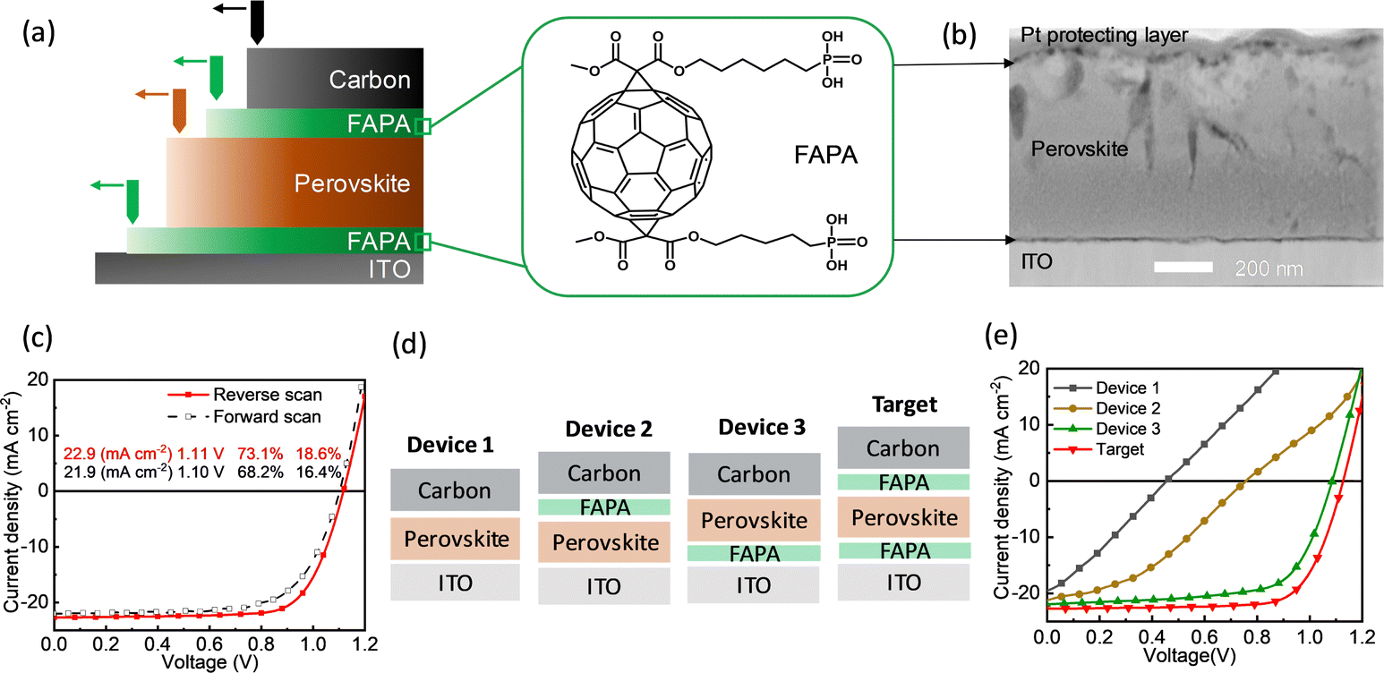 | ||
| Fig. 1 Architecture and performance of solar cells. (a) Schematic drawing of PSCs fabrication and the chemical structure of FAPA. (b) Cross-sectional TEM images of the PSCs based on the FAPA layer. The carbon counter electrode is replaced by a platinum (Pt) protecting layer for the convenience of cross-sectional lamella preparation. (c) J–V curves of the champion PSC adopting FAPA/perovskite/FAPA architecture, measured from the reverse-scan direction and forward-scan direction. (d) Schematic drawing of PSC architectures with the FAPA layer partially or fully removed. (e) J–V curves of the PSCs with the different architectures shown in (d). | ||
To demonstrate the critical role of the FAPA layers in reinforcing charge selectivity, we investigate the variation in solar cell performance with one or both FAPA layers removed from the interfaces (Fig. 1d). The J–V curves, Fig. 1e, show an immediate disappearance of rectification when the bottom FAPA layer is removed (Device 2), and more so when both FAPA layers are taken out (Device 1). By removing only the top FAPA layer, the rectification behavior of the J–V curve is mostly maintained (Device 3) but moderate losses of VOC and FF are observed compared to the target device (double FAPA). If the FAPA layers applied either above or below the perovskite are too thick, the J–V curves exhibit significant charge resistance (Fig. S2, ESI†). We summarize the statistical data of the PV parameters from approximately 60 devices for each of the architectures in Table 1. The results show the critical role of the FAPA layer in providing electron selectivity for the ITO/perovskite interface. In the meantime, the same FAPA layer, when deposited on top of the perovskite, shows a moderate but still noticeable enhancement in hole selectivity for the perovskite/carbon interface.
| Device structure | J sc (mA cm−2) | V OC (mV) | FF (%) | PCE (%) |
|---|---|---|---|---|
| Device 1 | 17.5 ± 3.5 | 618 ± 212.8 | 28.3 ± 9.7 | 3.7 ± 3.6 |
| Device 2 | 18.0 ± 3.6 | 623 ± 221.5 | 30.5 ± 9.1 | 4.1 ± 3.4 |
| Device 3 | 22.1 ± 0.5 | 1061 ± 19.9 | 67.9 ± 5.6 | 15.9 ± 1.8 |
| Target | 22.1 ± 0.7 | 1120 ± 4.1 | 71.9 ± 1.1 | 17.8 ± 0.5 |
Before investigating the mechanism of charge-selectivity formation, we first probe the respective chemical interactions of FAPA on ITO and on the perovskite surface through X-ray photoelectron spectroscopy (XPS). The full XPS of ITO with and without FAPA are shown in Fig. S3 (ESI†). Deposition of the FAPA layer on ITO results in the emergence of a characteristic peak for phosphorus (Fig. S4, ESI†). In Fig. 2a, we look in more detail into the selected spectra of the In 3d and O 1s core levels measured from the ITO to probe any chemical interaction. The In 3d peak shows a significant decrease in peak intensity upon the deposition of FAPA, implying the formation of a dense FAPA layer on ITO. Moreover, an obvious shift of the In 3d peak to higher binding energy after coating with SAM indicates changes in the electron density around the indium atoms, which is caused by the strong interaction between the phosphonic acid and indium. The formation of a SAM layer is also confirmed by the strong signals of C–O– and P–O– bonds in the XPS O 1s peak shown in Fig. 2b. Both the reduction in intensity of the –OH groups and the shift of the In 3d peak indicate the strong chemical reaction between phosphonic acids and the hydroxyl groups at the ITO surface.24
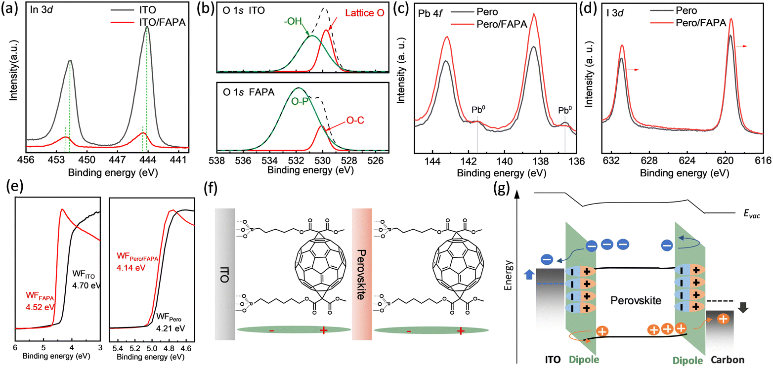 | ||
| Fig. 2 Surface binding scheme and interfacial energetic alignment. (a) XPS In 3d spectra and (b) O 1s spectra measured at the surfaces of bare ITO and of FAPA-coated ITO. (c) XPS Pb 4f spectra and (d) I 3d spectra measured from the surface of a perovskite and a FAPA-coated perovskite film. (e) UPS spectra of ITO, ITO/FAPA, perovskite and perovskite/FAPA surfaces. The WF of each layer evaluated from the cut-off energies in the spectra are denoted in the figure. (f) Schematic drawing of the preferential binding of the FAPA molecules at the surfaces of ITO and perovskite, respectively. (g) Schematic drawing of the band diagram of the FAPA-perovskite-FAPA solar cell. The energetic positions of the LUMO and HOMO of the FAPA layer and the perovskite are determined by UPS and optical absorption spectra as shown in Fig. S5 and S6 (ESI†). | ||
When depositing FAPA on the surface of the perovskite film, the intensity of the Pb2+ 4f peak at binding energies of 138.4 and 143.2 eV increases significantly, while the peaks corresponding to the metallic Pb0 cluster phase at ca.136.6 and 141.5 eV, caused by the decomposition of perovskite,25 decrease, as shown in Fig. 2c. That indicates that FAPA on top of the perovskite suppresses the formation of metallic Pb0 during the annealing process due to partial replacement of weakly coordinated Pb2+ by the SAM, and thus prevents perovskite degradation during processing. The I 3d XPS peak in Fig. 2d exhibits a shift to lower binding energy, from 619.5 eV to 619.4 eV, suggesting an increase in electron density at the perovskite surface due to the anchoring of the phosphonic acid functional group. The results support our hypothesis that the FAPA layer has significant interactions with both ITO and perovskite surfaces.
As a consequence of FAPA binding to the surface, the surface WF of the ITO and the perovskite are altered, as measured through ultraviolet photoelectron spectroscopy (UPS), plotted in Fig. 2e. The UPS results show a decrease in WF from −4.70 to −4.52 eV for the ITO substrate, and a decrease from −4.21 to −4.14 eV for the perovskite upon the deposition of FAPA layers on their surfaces, whereas an increase from −4.28 to −4.41 eV is observed for the carbon electrode with the FAPA on top (Fig. S7, ESI†). We propose that the decrease in WF is induced by the formation of a dipole layer at the respective interfaces as shown in Fig. 2f. Due to the extended layer thickness of the SAM, the magnitude of the measured dipole effect might be partially screened. However, the direction of the electrical field formed at the surfaces can be indicated. A WF decrease from the surface of ITO to the surface of the SAM corresponds to a dipole with the negative charge density at ITO and the positive charge density at the surface of the SAM. This leads to an attractive force for electron charges at the interface,24 depicted by a partial downward bending of the perovskite conduction band in Fig. 2g. A similar argument holds for the interface to the carbon electrode. The decrease of the WF from the surface of the perovskite to the surface of the SAM suggests a higher electron density at the surface of the perovskite and a higher hole density at the surface of the SAM. We also determine the highest occupied molecule orbital (HOMO) of FAPA to be −5.78 eV from the UPS measurement, and the lowest unoccupied molecule orbital level (LUMO) to be −3.68 eV from measurement of the FAPA's optical bandgap, Fig. S5 (ESI†).
We then turn to investigate how the change in energetic alignment affects charge carrier recombination at the respective interfaces. Time-resolved photoluminescence (trPL) was measured on the respective half cells. The perovskite film in direct contact with ITO, in Fig. 3a, exhibits a rather fast PL decay, indicating the dominance of non-radiative surface recombination. Upon inserting the FAPA dipole layer, the PL transient kinetics is slowed down from 53 ns to 691 ns, suggesting effective suppression of perovskite surface recombination by the dipole layer, which may also indicate a slight passivation effect. Interface recombination is slightly slower at the contact with the carbon electrode, as already found by the rather high VOC values for Target compared to Device 3 (Table 1). Consequently, the insertion of the FAPA dipole layer results in a moderate decrease in recombination kinetics as shown in Fig. 3b. The results highlight that the non-radiative recombination takes place mainly at the ITO/perovskite interface, which is remarkably suppressed with the ITO/FAPA/perovskite configuration, whilst the top FAPA layer only moderately suppresses the non-radiative recombination at the perovskite/carbon interface.
 | ||
| Fig. 3 Impact of interfacial energetic alignment on charge carrier dynamics. (a) Time-resolved PL spectra of ITO/perovskite and ITO/FAPA/perovskite films. (b) Time-resolved PL spectra of perovskite/carbon and perovskite/FAPA/carbon films, both deposited on glass substrates. (c) PLQY (grey) and QFLS (red) of the different layer stacks. (d) Dark J–V curves of an ITO/FAPA/perovskite/FAPA/carbon solar cell and of an ITO/perovskite/carbon solar cell. | ||
The respective non-radiative recombination losses at both surfaces of the perovskite film are further quantified by measuring absolute photoluminescence quantum yields (PLQY) and the corresponding quasi-Fermi level splitting (QFLS) of different layer stacks, which are shown in Fig. 3c. The detailed calculation of QFLS is shown in Note S1 (ESI†). With the FAPA at the ITO/perovskite interface, there is a 12-fold increase in PLQY, correlating to a reduction of approximately 64 mV in VOC loss. Additionally, the external open circuit voltage loss is further reduced by the addition of FAPA on top of the perovskite layer. The results of PLQY are consistent with those of trPL, both underlining the suppression of non-radiative recombination by FAPA at either perovskite interface. To investigate how the variation of energetic alignment affects charge extraction and injection, we plot in Fig. 3d the dark current measurement. The target device with two SAM dipole layers shows a normal dark J–V curve that exhibits three distinct regions, dominated by recombination current at lower bias, by diffusion current at intermediate bias and by injection current at higher bias.26 In contrast, the device without dipole layers exhibits higher leakage current at low bias (<1 V) but lower injection current in the high-bias region (>2 V). This is consistent with our analysis above, indicating large energetic offsets at the interfaces that are remarkably reduced by the dipole layers.
Having shown the contact-layer design simplification for PSCs, we lastly demonstrate the suitability of the novel architecture for high-throughput fabrication. For R2R fabrication of perovskite PV, glass substrates are not viable and must be replaced by flexible ones. In Fig. 4a, we depict a comparative drawing of our novel FAPA-based device and of a conventional device architecture based on SnO2 as the ETL and PEDOT complex as the HTL, denoted as “reference”. The flexible substrate utilized in this study consists of an ITO-Ag-ITO (IMI) conductive layer deposited on polyethylene terephthalate (PET) plastic foil, denoted as PET-IMI hereafter. We plotted in Fig. 4b the statistical performance data of the target and reference PSCs fabricated on glass-ITO and plastic flexible substrates, respectively. The FAPA-based and the reference solar cells on glass-ITO substrates show an average PCE of 17.8 ± 0.5% and 14.5 ± 0.9%, respectively. When switching from glass-ITO to the PET-IMI substrate, there is a drop in the average PCE to 15.6 ± 0.8% for the target devices, whereas a much larger drop is observed for the reference devices, down to a PCE of 9.4 ± 1.4%. Concomitantly, a clear decrease in device reproducibility is seen for the reference device, manifested by a larger distribution width in PCE. We plotted in Fig. 4c the J–V curves of the best-performing cell for each condition, showing champion PCEs of the target and reference architectures of 18.6% versus 15.6%, respectively, on glass-ITO and 15.6% versus 10.7%, respectively, for PET-IMI. The results highlight that the novel FAPA-based architecture notably outperforms the conventional SnO2-based one, especially when fabricated on flexible substrates, which reduces the performance loss in the rigid-to-flexible substrate transfer required for R2R device fabrication.
 | ||
| Fig. 4 Device performance loss from rigid to flexible substrates. (a) SnO2-based (Ref) and FAPA-based (Target) device structures. (b) Statistic distribution of PV parameters of the Ref and Target devices. (c) J–V curves of the Ref and Target devices on glass-ITO and PET-IMI substrates. (d) Shelf-lifetime of a FAPA-based simplified device and a SnO2 based device in ambient air without encapsulation. (e) Normalized PCEs of f-PSCs as a function of the number of mechanical bending cycles. | ||
An investigation of the J–V curves and the resulting PV parameters shows that the rigid-to-flexible PCE loss observed for the SnO2-based device is dominated by the FF loss that can be correlated to shunting, as indicated by the enhanced slope of the J–V curves in Fig. 4c. In order to identify the reasons for the enhanced shunting in SnO2-based flexible devices, the film morphologies of SnO2 and FAPA on PET-IMI substrate are considered. The optical microscopic images, in Fig. S8 (ESI†), readily visualize the difference in film homogeneity on the different substrates: the SnO2 film shows visible aggregates on the glass-ITO substrate, which become more abundant on PET-IMI substrates, whereas smooth FAPA films can be deposited on both glass-ITO and PET-IMI, with no noticeable artefacts. The origin of the reduced film homogeneity is ascribed to the non-wetting behavior of SnO2 nanoparticles on the IMI-PET substrate which was verified by contact angle measurements. Fig. S9 (ESI†) shows that the contact angle of the aqueous dispersion of SnO2 nanoparticle is 65° at the glass-ITO surface and further increases to 77° at the PET-IMI surface (see images in Fig. S10, ESI†). In contrast, the alcoholic dispersion of FAPA molecules exhibits rather small contact angles of 10° on the glass-ITO surface and 13° on the PET-IMI surface and thus does not experience any wetting issues.
Alongside the smooth fabrication of FAPA and the application of carbon electrodes on top, the operational stability of the device was enhanced. In Fig. 4d, we demonstrate the shelf-lifetime of the FAPA-enabled target device compared to the SnO2-based reference. The target devices exhibit superior storage stability in ambient air, retaining 90% of their original PCE after 1200 hours, compared to 80% for the reference device. Moreover, under 1 sun illumination at 65 °C (ISOS-L-2l), the FAPA-simplified device maintains 85% of its initial PCE, whereas the SnO2-based reference retains only 65% after 200 h of accelerated aging (Fig. S11, ESI†). Additionally, the evolution of PCE during bending tests of the f-PSCs, Fig. 4e, highlights the improved mechanical stability of the FAPA-simplified device. After 3000 bending cycles with a bending radius of 5 mm, the devices maintain 95% of their initial PCE, while the reference SnO2 based devices show a lower retention of only 80%.
Having shown the improved processability on flexible substrates, we lastly demonstrate the improvement in process scalability of the FAPA-based devices over the conventional SnO2-based ones by extending device fabrication from solar cells to mini solar modules. The mini solar module consists of seven serially connected cells, with a total aperture area of 20.25 cm2 and an active area of 15.8 cm2. The schematic diagram of the interconnection of the solar module, Fig. 5a, shows the configuration of P1, P2, and P3 lines that are needed for electrical interconnection of the adjacent cells. In Fig. 5b, photographs of the flexible solar cell and of the flexible solar module are shown, with all layers in the devices being fabricated by coating under ambient environmental conditions, including the carbon counter-electrode.
 | ||
| Fig. 5 Up-scalability and mini-module demonstration. (a) Schematic drawing of the layer stack and the lateral layout of the solar module. (b) Photograph of the fully printed flexible FAPA-perovskite-FAPA solar cell and module. (c) Device performance losses from cells to modules on glass-ITO and PET-IMI substrates. (d) Champion J–V curves of FAPA and SnO2 based modules on the glass-ITO substrate. (e) Champion J–V curves of FAPA and SnO2 based modules on the PET-IMI substrate. | ||
The mini solar modules are fabricated on both glass-ITO and PET-IMI substrates, using the same layout of laser patterning. The scalability is then demonstrated through a comparison of the champion PCE of the mini solar module against that of the solar cell, Fig. 5c. All devices suffer from a PCE drop during upscaling from the 0.1 cm2 to 20.25 cm2 aperture area, but the decrease in PCE is notably lower in the FAPA-based devices than in SnO2-based devices. A decrease in average from 17.8% to 15.7% for the target devices versus 15.5% to 12.5% for the reference devices on the glass-ITO substrate, and a decrease in average from 15.6% to 11.3% for the target devices versus 12.1% to 5.5% for the reference devices on the PET-IMI substrate are observed. We plot in Fig. 5d and e a comparison of the J–V curves of the solar modules of the two architectures on different substrates, showing the key factor leading to PCE enhancement by FAPA-based architecture to be an increase in VOC and FF, which can be facilely ascribed to the improvement in contact-layer quality enabled by the novel device architecture. The reproducibility of f-PSMs enabled by FAPA optimization is further confirmed by the box plot comparison of each photovoltaic parameter to the SnO2-based reference, in Fig. S12 (ESI†).
Conclusions
In this work, we address two factors that hinder the development of scalable perovskite module production on flexible substrates, namely, the loss of device PCE when transferring device fabrication from a rigid to flexible substrate, and when transferring device fabrication from solar cells to solar modules. We propose a simplified contact-layer configuration that is based on SAM molecules capable of forming both p-type and n-type rectifying interfaces. The shifts in interfacial energetic alignment between the perovskite and the electrodes fulfill the role in maximizing charge extraction and minimizing perovskite surface recombination. We further elucidate that the chemical origin of the paired dipole formation is due to the strong coordination of the phosphonic acid group with metal ions, along with the alignment and polarity of the molecule. In the context of interface engineering, this approach appears to contradict conventional design rules. Taking a detailed look into the formation mechanisms, the novelty of this approach rather lies in the departure from traditional thinking than in any novel unknown effects. Nevertheless, this innovative approach not only surprises but also redefines the boundaries of what is possible with advanced interface engineering.The excellent processability of the alcohol dispersion on a flexible substrate and the simplified procedure of depositing one type of material for both interfaces jointly result in significantly reduced PCE loss when transferring device fabrication from a rigid to flexible substrate, and in a remarkable closing of the PCE gap from a flexible cell (0.1 cm2) to a flexible module (20.25 cm2). This allows us to demonstrate the champion PCEs of 16.3% and 11.3% for fully printed, flexible PSCs and PSMs with carbon electrodes, both standing at the cutting edge among their counterparts.
Author contributions
L. D. performed the experiments and wrote the manuscript. S. Q. contributed to the discussion of the manuscript. O. K. measured the XPS spectrum. M. W. technically support roll-to-roll line printing. S. F. was involved in discussions about fabrication techniques for flexible modules. J. G. C. designed the module layout. H. P. guided the UPS measurements. D. J. and C. L. measured and analyzed the PL data as well as V. M. C. J. T. measured the absolute PLQY. F. U. K. performed STEM measurements under the supervision of C. D. T. D., N. L. and F. Y. modified and polished the manuscript. C. J. B. reviewed and revised the manuscript. H.-J. E. supervised the work and the writing of the manuscript. All co-authors discussed the results and provided comments on the manuscript.Data availability
The data that support the findings of this study are available in the ESI.†Conflicts of interest
The authors declare no conflict of interest.Acknowledgements
The Solar Factory of the Future (SFF) as part of the Energy Campus Nürnberg (EnCN) is acknowledged, which is supported by the Bavarian State Government (FKZ 20.2-3410.5-4-5). Part of this work has been supported by the Helmholtz Association in the framework of the innovation platform “Solar TAP”. T. D. acknowledges the financial support from Deutsche Forschungsgemeinschaft (DFG) via the perovskite SPP2196 program (project no. 506698391). L. D., J. T. and C. L. gratefully acknowledge funding of the Erlangen Graduate School in Advanced Optical Technologies (SAOT) by the Bavarian State Ministry for Science and Art. L. D. acknowledges Sven Boelke and Ivana Mrsic for XPS measurements under the guidance of H. P. S. Q., J. T. and C. L. are grateful for the support from the China Scholarship Council (CSC). J. G. C. gratefully acknowledges the Deutscher Akademischer Austauschdienst (DAAD) for granting a doctoral scholarship. F. U. K. thanks the Jardine Foundation and Cambridge Trust for a doctoral scholarship. C. D. acknowledges European Union’s Horizon 2020 research and innovation program (823717–ESTEEM3). F. Y. acknowledges the financial support from the National Natural Science Foundation of China (grant no. 52102287), the Natural Science Foundation of Jiangsu Province (grant no. BK20210731), and the Natural Science Foundation of the Jiangsu Higher Education Institutions of China (21KJD150003).References
- N. L. Chang, A. Wing, Y. Ho-baillie, D. Vak, M. Gao, M. A. Green and R. J. Egan, Sol. Energy Mater. Sol. Cells, 2018, 174, 314 CrossRef CAS.
- F. Yang, D. Jang, L. Dong, S. Qiu, A. Distler, N. Li, C. J. Brabec and H. J. Egelhaaf, Adv. Energy Mater., 2021, 11, 2101973 CrossRef CAS.
- H. C. Weerasinghe, N. Macadam, J. E. Kim, L. J. Sutherland, D. Angmo, L. W. T. Ng, A. D. Scully, F. Glenn, R. Chantler, N. L. Chang, M. Dehghanimadvar, L. Shi, A. W. Y. Ho-Baillie, R. Egan, A. S. R. Chesman, M. Gao, J. J. Jasieniak, T. Hasan and D. Vak, Nat. Commun., 2024, 15, 1 Search PubMed.
- D. Beynon, E. Parvazian, K. Hooper, J. McGettrick, R. Patidar, T. Dunlop, Z. Wei, P. Davies, R. Garcia-Rodriguez, M. Carnie, M. Davies and T. Watson, Adv. Mater., 2023, 2208561 CrossRef CAS PubMed.
- L. J. Sutherland, D. Vak, M. Gao, T. A. N. Peiris, J. Jasieniak, G. P. Simon and H. Weerasinghe, Adv. Energy Mater., 2022, 12, DOI:10.1002/aenm.202202142.
- P. Primer, Nature, 2016, 539, 488 CrossRef PubMed.
- L. Lucera, P. Kubis, F. W. Fecher, C. Bronnbauer, M. Turbiez, K. Forberich, T. Ameri, H. J. Egelhaaf and C. J. Brabec, Energy Technol., 2015, 3, 373 CrossRef.
- Z. Li, T. R. Klein, D. H. Kim, M. Yang, J. J. Berry, M. F. A. M. Van Hest and K. Zhu, Nat. Rev. Mater., 2018, 3, 18017 CrossRef CAS.
- S. S. Shin, S. J. Lee and S. Il Seok, Adv. Funct. Mater., 2019, 29, 1900455 CrossRef CAS.
- P. Schulz, ACS Energy Lett., 2018, 3, 1287 CrossRef CAS.
- S. Y. Park and K. Zhu, Adv. Mater., 2022, 34, 1 Search PubMed.
- D. Richards, D. Burkitt, R. Patidar, D. Beynon and T. M. Watson, Mater. Adv., 2022, 3, 8588 RSC.
- S. Y. Lee, G. Y. Park, N. Y. Kim, M. Kang, K. Kim, S. K. Cho, W. Choi, J. S. Myung and D. S. Ham, Energy Technol., 2024, 12, 1 CAS.
- T. Bu, J. Li, F. Zheng, W. Chen, X. Wen, Z. Ku, Y. Peng, J. Zhong, Y. B. Cheng and F. Huang, Nat. Commun., 2018, 9, 1 CrossRef CAS.
- G. Lee, M. C. Kim, Y. W. Choi, N. Ahn, J. Jang, J. Yoon, S. M. Kim, J. G. Lee, D. Kang, H. S. Jung and M. Choi, Energy Environ. Sci., 2019, 12, 3182 RSC.
- D. Li, X. Dong, P. Cheng, L. Song, Z. Wu and Y. Chen, Adv. Sci., 2022, 9, 2203683 CrossRef CAS.
- S. Y. Kim, S. J. Cho, S. E. Byeon, X. He and H. J. Yoon, Adv. Energy Mater., 2020, 10, 1 Search PubMed.
- P. Piotrowski, A. Krogul-Sobczak and A. Kaim, J. Environ. Chem. Eng., 2019, 7, DOI:10.1016/j.jece.2019.103147.
- G. Qu, S. Cai, Y. Qiao, D. Wang, S. Gong, D. Khan, Y. Wang, K. Jiang, Q. Chen, L. Zhang, Y. G. Wang, X. Chen, A. K. Y. Jen and Z. X. Xu, Joule, 2024, 8, 2123 CrossRef CAS.
- P. J. Hotchkiss, S. C. Jones, S. A. Paniagua, A. Sharma, B. Kippelen, N. R. Armstrong and S. R. Marder, Acc. Chem. Res., 2012, 45, 337 CrossRef CAS.
- S. A. Paniagua, E. L. Li and S. R. Marder, Phys. Chem. Chem. Phys., 2014, 16, 2874 RSC.
- T. Du, S. Qiu, X. Zhou, V. M. Le Corre, M. Wu, L. Dong, Z. Peng, Y. Zhao, D. Jang, E. Spiecker, C. J. Brabec and H.-J. Egelhaaf, Joule, 2023, 7, 1920 CrossRef CAS.
- T. Du, C. H. Burgess, C.-T. Lin, F. Eisner, J. Kim, S. Xu, H. Kang, J. R. Durrant and M. A. McLachlan, Adv. Funct. Mater., 2018, 28, 1803943 CrossRef.
- L. Dong, S. Qiu and J. G. Cerrillo, Energy Environ. Sci., 2024 10.1039/D4EE01647E.
- T. Du, S. R. Ratnasingham, F. U. Kosasih, T. J. Macdonald, L. Mohan, A. Augurio, H. Ahli, C.-T. Lin, S. Xu, W. Xu, R. Binions, C. Ducati, J. R. Durrant, J. Briscoe and M. A. McLachlan, Adv. Energy Mater., 2021, 11, 2101420 CrossRef CAS.
- G. J. A. H. Wetzelaer, M. Scheepers, A. M. Sempere, C. Momblona, J. Ávila and H. J. Bolink, Adv. Mater., 2015, 27, 1837 CrossRef CAS.
Footnote |
| † Electronic supplementary information (ESI) available. See DOI: https://doi.org/10.1039/d4ee02707h |
| This journal is © The Royal Society of Chemistry 2024 |