Ferroelectricity in CsPb2Nb3O10 and exfoliated 2D nanosheets†
Yan
Li‡
a,
Masanari
Shimada‡
a,
Makoto
Kobayashi
 ab,
Eisuke
Yamamoto
 ab,
Ruben
Canton-Vitoria
bc,
Xiaoyan
Liu
d and
Minoru
Osada
 *abe
*abe
aDepartment of Materials Chemistry, Nagoya University, Nagoya 464-8601, Japan. E-mail: mosada@imass.nagoya-u.ac.jp
bInstitute of Materials and Systems for Sustainability (IMaSS), Nagoya University, Nagoya 464-8601, Japan
cJoining and Welding Research Institute, Osaka University, Osaka 567-0047, Japan
dChongqing Key Laboratory of Nano/Micro Composites and Devices, College of Metallurgy and Materials Engineering, Chongqing University of Science and Technology, Chongqing 401331, China
eResearch Institute for Quantum and Chemical Innovation, Institutes of Innovation for Future Society, Nagoya University, Nagoya 464-8601, Japan
First published on 23rd September 2024
Abstract
Pb-based perovskites play pivotal roles in ferroelectric research. In the search for new Pb-based ferroelectrics, we investigated the ferroelectric properties of Dion–Jacobson type CsPb2Nb3O10 and exfoliated 2D nanosheets. Ferroelectricity in CsPb2Nb3O10 was demonstrated for the first time. CsPb2Nb3O10 adopted a polar tetragonal structure with a modest TC = 260 °C and polarization PS = 7.93 μC cm−2; the polarization mainly arose from the out-of-plane displacements of Nb5+ ions and nearby oxygens. CsPb2Nb3O10 layered perovskite offers additional advantages for tailoring ferroelectric nanomaterials, as exfoliated 2D nanosheets provide novel platforms for investigating ferroelectric properties down to the 2D limit. Piezoresponse force microscopy confirmed stable ferroelectricity even in exfoliated 2D Pb2Nb3O10 nanosheets.
Introduction
Lead (Pb) is a magic element for ferroelectric materials. Pb-based perovskites have always played pivotal roles in the history of ferroelectric science and technology. One of the most important materials is PbTiO3, where ferroelectric polarization is linked to the off-centering of Ti4+ ions in TiO6 octahedra due to so-called second-order Jahn–Teller effects.1,2 In PbTiO3, Pb2+ ions on the A site also contribute to this off-centering, influenced by the unique characteristics of 6s2 lone-pair electrons.3,4 These lone-pair electrons on Pb2+ ions play a significant role in the structural and physical properties of Pb-based perovskites; the strong covalent nature of Pb–O bonds and steric hindrances of Pb2+ ions contribute to a large polarization with a high Curie temperature (TC) of 490 °C.5–7Similar lone-pair effects are expected in layered perovskites containing Bi3+ and Pb2+ ions with lone-pair electrons. Significant efforts have been devoted to developing new ferroelectric materials, focusing on Bi-based layered perovskites with Aurivillius (AU) structures (e.g., Bi4Ti3O12)8,9 and Dion–Jacobson (DJ) structures (e.g., RbBiNb2O7, CsBi2Ti2NbO10)10,11 as primary targets for Pb-free high-TC ferroelectrics due to environmental concerns. While Pb-based compounds remain important targets, Pb-based layered perovskites have been rarely synthesized to date. Experimental confirmation of ferroelectricity has been achieved in AU-type Bi-layered perovskites (PbBi2Ta2O9, PbBi4Ti4O15, and Pb2Bi4Ti5O18).12–14
Our primary concern is that new solutions can be found in the DJ-type layered perovskite CsPb2Nb3O10, which has been first reported in 1988 (ref. 15). Although pioneering studies on dielectric properties appeared in 1999 (ref. 16), this compound has neither been characterized nor documented in the ferroelectric database. Furthermore, DJ-type layered perovskites offer additional advantages for ferroelectric research, as exfoliated 2D nanosheets provide novel platforms for investigating ferroelectric properties down to the 2D limit. While the exfoliation of Rb-analogue (RbPb2Nb3O10) has been reported by several groups,17–19 previous research on Pb2Nb3O10 nanosheets has primarily focused on photo-functionalities such as solar cells and photocatalysts. Exfoliated Pb2Nb3O10 nanosheets have not yet been explored as 2D ferroelectrics. If CsPb2Nb3O10 and its exfoliated 2D nanosheets exhibit ferroelectricity, how does the reduced dimensionality affect their ferroelectric properties? These questions are particularly intriguing from both fundamental and practical perspectives, as CsPb2Nb3O10 could potentially illuminate new properties of Pb-based perovskites.
Here, we present the characterization of the structural and ferroelectric properties of CsPb2Nb3O10. Our findings demonstrate that CsPb2Nb3O10 exhibits ferroelectric behaviour with a moderate Curie temperature (TC) of 260 °C and a spontaneous polarization (PS) of 7.93 μC cm−2. Piezoresponse force microscopy (PFM) reveals that the ferroelectric properties remain stable even in exfoliated 2D nanosheets.
Results and discussion
Synthesis and structural characterizations of CsPb2Nb3O10
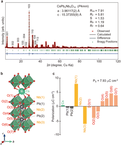
CsPb2Nb3O10 was synthesized via solid-state reaction at 1000 °C for 24 h in air (see Experimental in ESI†). Powder X-ray diffraction (XRD) confirmed that CsPb2Nb3O10 crystallized in the tetragonal system (Fig. 1a and b); detailed structural features will be discussed later. The formation of CsPb2Nb3O10 was further verified using field emission scanning electron microscopy (FE-SEM) equipped with energy-dispersed X-ray spectroscopy (EDS) (Fig. S1, ESI†). FE-SEM observations revealed a plate morphology characteristic of layered perovskites. EDS analysis confirmed the composition of the product as Cs1.03Pb2.20Nb3.00, consistent with CsPb2Nb3O10.To investigate the detailed structure, single-crystal XRD measurements were performed on CsPb2Nb3O10. A single crystal with dimension of 0.02 × 0.16 × 0.29 mm3 was selected for the XRD analysis. The crystal structure was characterized by the direct method with the SHELXT software. The XRD pattern was successfully refined with P-lattice symmetry, and possible space groups included P4/mmm, P4mm, P![[4 with combining macron]](https://www.rsc.org/images/entities/char_0034_0304.gif) m2, P422 or P
m2, P422 or P![[4 with combining macron]](https://www.rsc.org/images/entities/char_0034_0304.gif) 2m. Second harmonic generation (SHG) measurements (Fig. S2, ESI†) indicated that CsPb2Nb3O10 exhibited SHG activity, suggesting a polar non-centrosymmetric structure (Fig. 1b). Considering the polar nature, CsPb2Nb3O10 adopted a tetragonal system with the polar space group P4mm (no. 99).
2m. Second harmonic generation (SHG) measurements (Fig. S2, ESI†) indicated that CsPb2Nb3O10 exhibited SHG activity, suggesting a polar non-centrosymmetric structure (Fig. 1b). Considering the polar nature, CsPb2Nb3O10 adopted a tetragonal system with the polar space group P4mm (no. 99).
We calculated the polarization (PS) value based on the structural data (Fig. 1b) using the formula:11,20
Ferroelectric properties of CsPb2Nb3O10
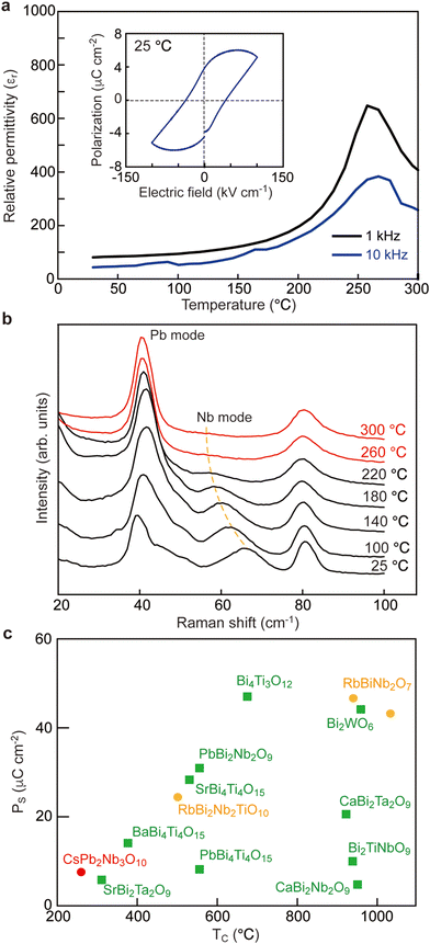
To investigate the dielectric and ferroelectric properties, we performed electrical characterization using a ceramic pellet of CsPb2Nb3O10 (Fig. 2). Polarization–electric field (P–E) measurements confirmed a well-saturated ferroelectric hysteresis loop at room temperature (Fig. 2a, inset). The remanent polarization (Pr) value was 4 μC cm−2, consistent with the PS value (7.93 μC cm−2) calculated from the structural data. Clear polarization switching behavior was also observed in piezoelectric response measurements, with a bipolar strain curve displaying a characteristic butterfly strain loop (Fig. S3, ESI†). The piezoelectric coefficient was estimated from the formula d33 = Smax/Emax, where Emax and Smax are the maximum applied electric field and corresponding unipolar strain output the piezoelectric coefficient, respectively. The piezoelectric coefficient (d33) was determined to be 14.3 pm V−1, a value relatively modest compared to simple perovskites like PbTiO3. The temperature dependence of the dielectric constant (εr) in CsPb2Nb3O10 was examined to elucidate its phase transition behavior (Fig. 2a). The dielectric constant exhibited a transition with a broad maximum occurring at 260 °C, where the TC value was estimated. The εr–T curves showed no clear frequency dependence, similar to behaviors observed in conventional ferroelectrics. | ||
| Fig. 2 Ferroelectric properties of CsPb2Nb3O10. (a) εr–T curves measured at 1 and 10 kHz. (Inset) P–E loop at 25 °C. (b) Temperature dependence of low-frequency Raman spectra. (c) Relationship between the polarization and the TC value for CsPb2Nb3O10 and previously reported Bi and Pb-based layered perovskites.9–14,25–29 The symbols represent AU (squares) and DJ-type perovskites (circles), respectively. | ||
To gain a deeper insight into the structural origin of the observed ferroelectric responses, we measured the temperature-dependent Raman spectra of CsPb2Nb3O10 (Fig. 2b). At room temperature, CsPb2Nb3O10 exhibited intense phonon modes (at 40–80, 180–260, ∼580, ∼700, and ∼960 cm−1) and many weak features (Fig. S4, ESI†). These modes and general spectral features were similar to those observed in other layered perovskites.21–24 In CsPb2Nb3O10, the Raman modes of CsPb2Nb3O10 could be classified as lattice vibrations involving the cations (<200 cm−1) and internal modes of the NbO6 octahedra (>200 cm−1). In this study, we discuss low-frequency modes related to polar displacements. Upon heating, some distinctive changes were observed in the low-frequency region, particularly for the low-frequency mode (at 65 cm−1). The 65 cm−1 mode exhibited gradual softening upon heating and disappeared at ∼260 °C. These changes resembled the so-called “soft-mode” behaviour observed in a typical displacive-type ferroelectric transition (proper ferroelectricity). Since the polarization mainly originated from the out-of-plain displacements of Nb5+ ions and nearby oxygens (O(4,5) and O(6,7) sites), the soft mode was strongly coupled with polar displacements of Nb5+ ions.
In Fig. 2c, we compare the TC and PS values among CsPb2Nb3O10 and previously reported Bi and Pb-based layered perovskites.9–14,25–29 As documented in previous literature, PbTiO3 exhibits both a high PS value (75 μC cm−2) and a high TC (490 °C) due to the strong covalent nature of Pb–O bonds and steric hindrances of Pb2+ ions. Triple-layered perovskites such as Bi4Ti3O12 and CsBi2Ti2NbO10 also show similar properties with high PS and TC value. In contrast, CsPb2Nb3O10 was quite unique; it exhibited a modest TC of 260 °C and polarization PS of 7.93 μC cm−2 possibly due to the negligible contribution of Pb2+ ions to the polarization. Regarding CsPb2Nb3O10, a distinctive feature was its insensitivity of the lowest-frequency mode at 40 cm−1 (Fig. 2b). In typical ferroelectrics like Bi4Ti3O12, the lowest-frequency mode strongly correlates with polar displacements of the heaviest Bi3+ ions.10,30 From the mass consideration of phonon modes, the lowest-frequency mode at 40 cm−1 would normally be expected to couple with the heaviest Pb2+ ions. The insensitivity of the Pb mode is indicative of weak lone-pair effects, consistent with the modestly high PS and TC values observed.
Ferroelectric properties of exfoliated 2D nanosheets
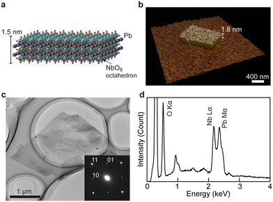
The exfoliation reaction of DJ compounds has research significance because exfoliated perovskite nanosheets offer novel platforms for investigating ferroelectric properties down to 2D limit.31,32 Having established the ferroelectric CsPb2Nb3O10, we synthesized Pb2Nb3O10 nanosheets via an intercalation-based exfoliation method involving acid treatment and bulky guest intercalation33,34 (Fig. S5, ESI†). Through acid treatment, the Cs+ ions in CsPb2Nb3O10 were replaced by H+ ions, resulting in the formation of a protonic phase (HPb2Nb3O10) while maintaining the layer structure. From the EDS analysis, the composition of the product was Pb2.06Nb3.00, indicating the success of cation exchange (Fig. S6, ESI†). Intercalation of tetrabutylammonium (TBA+) ions to the protonated compound resulted in total delamination into Pb2Nb3O10 nanosheets (Fig. 3a).The morphological and structural features of Pb2Nb3O10 nanosheets were investigated using atomic force microscopy (AFM) and transmission electron microscopy (TEM). AFM images revealed a sheet-like morphology with a thickness of 1.8 nm and lateral dimensions of ∼1 μm (Fig. 3b). This thickness corresponded to the crystallographic thickness of the Pb2Nb3O10 nanosheet, with slight differences due to adsorbed TBA+/H+ ions and water molecules. TEM analysis confirmed the high crystallinity of the 2D nanosheets (Fig. 3c). The selected area electron diffraction (SAED) pattern (Fig. 3c, inset) displayed a single-crystal-like pattern with distinct sharp spots, which can be indexed to the square cell structure characteristic of the 2D host layer in the parent CsPb2Nb3O10. The successful formation of Pb2Nb3O10 nanosheets was further validated by EDS (Fig. 3d), demonstrating that the composition was retained throughout the exfoliation process. These findings confirm the successful synthesis of Pb2Nb3O10 nanosheets.
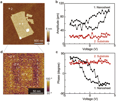
For the ferroelectric characterization, we conducted piezoresponse force microscopy (PFM) measurements on individual Pb2Nb3O10 nanosheets (Fig. 4).35 The nanosheets displayed a typical butterfly loop in the amplitude–voltage curve (Fig. 4b). The piezoelectric coefficient for Pb2Nb3O10 nanosheets was 5 pm V−1, which was smaller than that of 3D bulk CsPb2Nb3O10 (13 pm V−1) (Fig. S7, ESI†). In the phase–voltage curve, we observed 120° phase flipping at coercive voltages of ±2 V (Fig. 4c), indicating the robust ferroelectric switching behaviour of the Pb2Nb3O10 nanosheets. Furthermore, both the amplitude and phase curves exhibited identical coercive voltages (±2 V), confirming the ferroelectric nature of the Pb2Nb3O10 nanosheets.
To further investigate the switching behaviour, we performed PFM lithography of the Pb2Nb3O10 nanosheets was taken after writing a box-in-box pattern with reversed DC bias (Fig. 4d). The PFM image showed a clear reversal of phase contrast, indicating the polarization switching. Ferroelectric properties can often be affected by leakage current. However, the Pb2Nb3O10 exhibited highly insulating behaviour, indicating that its ferroelectric response was not a consequence of leakage current. Notably, the Pb2Nb3O10 nanosheet showed strong dielectric endurance with withstand voltages of 4.0 V and −4.5 V (Fig. S8, ESI†), attributed to its 2D size effects. This highly insulating nature is favorable for maintaining stable ferroelectricity even in Pb2Nb3O10 nanosheets.
For understanding the impact of dimensional reduction on ferroelectric properties, we performed additional PFM measurements of samples with different thicknesses (Fig. S9, ESI†). By comparing the PFM amplitude of samples with different thicknesses, the PFM amplitude reduced with the layer thickness, consistent with size effect commonly found in ferroelectric thin films.36,37 The critical thickness for ferroelectricity in perovskite materials has been thoroughly explored using different experimental methods, such PFM, TEM, Raman spectroscopy, and synchrotron XRD. Research indicates that ferroelectric polarization is notably diminished in thin films with fewer than 10 unit cells (∼4 nm). However, ferroelectric properties have been observed even in films as thin as 4–7.5 unit cells (1.6–3 nm) for BaTiO3,38–40 3–10 unit cells (1.2–4 nm) for PbTiO3,41 1.5 unit cells (around 0.6 nm) for PbZr0.2T0.8O3,42 and 7.5 unit cells (about 3 nm) for BiFeO3.43 Recent TEM studies have suggested that ultrathin PbZr0.2T0.8O3 films might not exhibit a critical thickness or size-dependent effects, with observed polarization values of approximately 22 μC cm−2 for films with 2.5 unit cells and 16 μC cm−2 for films with 1.5 unit cells.42 Despite these findings, determining the minimum thickness at which perovskite layers can retain ferroelectricity remains challenging due to the difficulties in synthesizing nearly perfect ultrathin perovskite films. Our research presents new opportunities to explore perovskite ferroelectrics with minimal critical thickness, as evidenced by the successful experimental confirmation of ferroelectricity in a 1.8 nm thick (3 unit cells) Pb2Nb3O10 nanosheet, marking it as the thinnest free-standing perovskite with confirmed ferroelectric properties.
Conclusions
We investigated the ferroelectric properties of DJ-type CsPb2Nb3O10 and its exfoliated 2D nanosheets. Ferroelectricity of CsPb2Nb3O10 was demonstrated for the first time. CsPb2Nb3O10 adopted a polar tetragonal structure with a moderate TC of 260 °C and polarization PS of 7.93 μC cm−2, primarily arising from the out-of-plane displacements of Nb5+ ions and nearby oxygens. Importantly, the contribution from Pb2+ ions was nearly negligible, contrasting with observations in Bi4Ti3O12 and CsBi2Ti2NbO10. Having established the ferroelectric CsPb2Nb3O10, we synthesized Pb2Nb3O10 nanosheets via an intercalation-based exfoliation method. Through PFM measurements, we found that ferroelectricity remained stable even in the exfoliated 2D Pb2Nb3O10 nanosheets. Our study opens new avenues for investigating 2D perovskite ferroelectrics at critical thicknesses.Compared with conventional ferroelectrics in bulk and thin-film forms, 2D ferroelectric nanosheets have various advantages such as high capacitance density, low voltage operation, flexibility and bandgap tunability, which are suitable for technological applications, such as non-volatile memories, field-effect transistors, sensors and energy harvesting devices. Furthermore, the self-assembly of 2D nanosheets can provide a potentially useful route to ferroelectric nanodevices with precisely controlled thickness and properties. These studies are currently underway.
Data availability
The data supporting this article have been included as part of the ESI† at [https://doi.org/10.1039/x0xx00000x].• Experimental section.
• FE-SEM image and EDS spectrum of CsPb2Nb3O10; SHG spectra; S–E curve; Raman spectra; exfoliation process; FE-SEM image and EDS spectrum of HPb2Nb3O10; PFM images of CsPb2Nb3O10 single crystal; I–V curve of Pb2Nb3O10 nanosheets; PFM signals from 3L film of Pb2Nb3O10 nanosheets; thickness dependence.
• Powder X-ray crystallographic data of CsPb2Nb3O10 (CIF).
Conflicts of interest
There are no conflicts to declare.Acknowledgements
This work was funded by the Grant-in-Aid for Scientific Research KAKENHI (21H05015, 22H01907, 23K17956), Japan Society for the Promotion of Science (JSPS), Design & Engineering by Joint Inverse Innovation for Materials Architecture (DEJI2MA), MEXT, and the joint usage/research program of the Institute of Materials and Systems for Sustainability (IMaSS), Nagoya University.References
- R. E. Cohen, Nature, 1992, 358, 136 CrossRef CAS.
- B.-G. Kim, S. M. Cho, T.-Y. Kim and H. M. Jang, Phys. Rev. Lett., 2001, 86, 3404 CrossRef CAS PubMed.
- Y. Kuroiwa, S. Aoyagi, A. Sawada, J. Harada, E. Nishibori, M. Takata and M. Sakata, Phys. Rev. Lett., 2001, 87, 217601 CrossRef CAS.
- T. Abe, S. Kim, C. Moriyoshi, Y. Kitanaka, Y. Noguchi, H. Tanaka and Y. Kuroiwa, Appl. Phys. Lett., 2020, 117, 252905 CrossRef CAS.
- G. Shirane, R. Pepinsky and B. C. Frazer, Acta Crystallogr., 1956, 9, 131 CrossRef CAS.
- S. C. Abrahams, S. K. Kurtz and P. B. Jamieson, Phys. Rev., 1968, 172, 551 CrossRef CAS.
- V. Gavrilyachenko, R. Spinko, M. Ma and E. Fesenko, Fiz. Tverd. Tela, 1970, 12, 1532 CAS.
- S. E. Cummins and L. E. Cross, J. Appl. Phys., 1968, 39, 2268 CrossRef CAS.
- Y. Noguchi and M. Miyayama, Appl. Phys. Lett., 2001, 78, 1903 CrossRef CAS.
- B.-W. Li, M. Osada, T. C. Ozawa and T. Sasaki, Chem. Mater., 2012, 24, 3111 CrossRef CAS.
- E. E. McCabe, E. Bousquet, C. P. J. Stockdale, C. A. Deacon, T. T. Tran, P. S. Halasyamani, M. C. Stennett and N. C. Hyatt, Chem. Mater., 2015, 27, 8298 CrossRef CAS.
- E. C. Subbarao, J. Phys. Chem. Solids, 1962, 23, 665 CrossRef CAS.
- Y.-I. Park, M. Miyayama and T. Kudo, J. Ceram. Soc. Jpn., 1999, 107, 413 CrossRef CAS.
- S. Dubey and R. Kurchania, Bull. Mater. Sci., 2015, 38, 1881 CrossRef CAS.
- M. A. Subramanian, J. Gopalakrishnan and A. W. Sleight, Mater. Res. Bull., 1988, 23, 837 CrossRef CAS.
- M. Fang, C. H. Kim and T. E. Mallouk, Chem. Mater., 1999, 11, 1519 CrossRef CAS.
- Y. Hu and L. Guo, ChemCatChem, 2015, 7, 584 CrossRef CAS.
- B. Zheng, L. Mao, J. Shi, Q. Chen, Y. Hu, G. Zhang, J. Yao and Y. Lu, Int. J. Hydrogen Energy, 2021, 46, 34276 CrossRef CAS.
- Y. Zhang, J. Yao, Z. Zhang, R. Zhang, L. Li, Y. Teng, Z. Shen, L. Kang, L. Wu and X. Fang, J. Mater. Sci. Technol., 2023, 164, 95 CrossRef CAS.
- Y. Shimakawa, Y. Kubo, Y. Nakagawa, S. Goto, T. Kamiyama, H. Asano and F. Izumi, Phys. Rev. B, 2000, 61, 6559 CrossRef CAS.
- J. M. Jehng and I. E. Wachs, Chem. Mater., 1991, 3, 100 CrossRef CAS.
- R. Nozaki, J. N. Kondo, C. Hirose, K. Domen, A. Wada and Y. Morioka, J. Phys. Chem. B, 2001, 105, 7950 CrossRef CAS.
- B.-W. Li, M. Osada, Y. Ebina, T. C. Ozawa, R. Ma and T. Sasaki, Appl. Phys. Lett., 2010, 96, 182903 CrossRef.
- S. Pal, S. Das, R. Nagarajan and S. Uma, J. Mater. Chem. C, 2022, 10, 14675 RSC.
- Q. Hou, B. Yang, C. Ma, Z. Zhou, R. Liang, H. Li and X. Dong, Ceram. Int., 2022, 48, 16677 CrossRef CAS.
- T. Zeng, X. Yu, S. Hui, Z. Zhou and X. Dong, Mater. Res. Bull., 2015, 68, 271 CrossRef CAS.
- Y. Noguchi, M. Miyayama, K. Oikawa, T. Kamiyama, M. Osada and M. Kakihana, Jpn. J. Appl. Phys., 2002, 41, 7062 CrossRef CAS.
- H. Irie, M. Miyayama and T. Kudo, J. Am. Ceram. Soc., 2000, 83, 2699 CrossRef CAS.
- I.-S. Yi and M. Miyayama, Mater. Res. Bull., 1997, 32, 1349 CrossRef CAS.
- M. Osada, M. Tada, M. Kakihana, T. Watanabe and H. Funakubo, Jpn. J. Appl. Phys., Part 1, 2001, 40, 5572 CrossRef CAS.
- M. Osada and T. Sasaki, Adv. Mater., 2012, 24, 210 CrossRef CAS PubMed.
- M. Osada and T. Sasaki, APL Mater., 2019, 7, 120902 CrossRef.
- Y. Ebina, T. Sasaki and M. Watanabe, Solid State Ionics, 2002, 151, 177 CrossRef CAS.
- Y. Ebina, K. Akatsuka, K. Fukuda and T. Sasaki, Chem. Mater., 2012, 24, 4201 CrossRef CAS.
- B. J. Rodriguez, C. Callahan, S. V. Kalinin and R. Proksch, Nanotechnology, 2007, 18, 475504 CrossRef.
- J. Junquera and P. Ghosez, Nature, 2003, 422, 506 CrossRef CAS PubMed.
- M. Stengel and N. A. Spaldin, Nature, 2006, 443, 679 CrossRef CAS.
- K. Hagiwara, K. N. Byun, S. Morita, E. Yamamoto, M. Kobayashi, X. Liu and M. Osada, Adv. Electron. Mater., 2023, 9, 2201239 CrossRef CAS.
- D. A. Tenne, P. Turner, J. D. Schmidt, M. Biegalski, Y. L. Li, L. Q. Chen, A. Soukiassian, S. Trolier-McKinstry, D. G. Schlom, X. X. Xi, D. D. Fong, P. H. Fuoss, J. A. Eastman, G. B. Stephenson, C. Thompson and S. K. Streiffer, Phys. Rev. Lett., 2009, 103, 177601 CrossRef CAS PubMed.
- Z. Wen, C. Li, D. Wu, A. Li and N. Ming, Nat. Mater., 2013, 12, 617 CrossRef CAS.
- D. D. Fong, G. B. Stephenson, S. K. Streiffer, J. A. Eastman, O. Auciello, P. H. Fuoss and C. Thompson, Science, 2004, 304, 1650 CrossRef CAS.
- P. Gao, Z. Zhang, M. Li, R. Ishikawa, B. Feng, H.-J. Liu, Y.-L. Huang, N. Shibata, X. Ma, S. Chen, J. Zhang, K. Liu, E.-G. Wang, D. Yu, L. Liao, Y.-H. Chu and Y. Ikuhara, Nat. Commun., 2017, 8, 15549 CrossRef CAS.
- Y. H. Chu, T. Zhao, M. P. Cruz, Q. Zhan, P. L. Yang, L. W. Martin, M. Huijben, C. H. Yang, F. Zavaliche, H. Zheng and R. Ramesh, Appl. Phys. Lett., 2007, 90, 252906 CrossRef.
Footnotes |
| † Electronic supplementary information (ESI) available. See DOI: https://doi.org/10.1039/d4dt02343a |
| ‡ These two authors contributed equally to this work. |
| This journal is © The Royal Society of Chemistry 2024 |


