Self-powered photodetectors: a device engineering perspective
Varun
Goel
 a,
Yogesh
Kumar
 a,
Gopal
Rawat
 b and
Hemant
Kumar
 *a
*a
aDepartment of Electronics and Communication Engineering, Jaypee Institute of Information Technology, Noida, India. E-mail: varun.goel@jiit.ac.in; yogesh.kumar@jiit.ac.in; hemant.kumar@jiit.ac.in
bSchool of Computing and Electrical Engineering, Indian Institute of Technology, Mandi, India. E-mail: gopal@iitmandi.ac.in
First published on 9th April 2024
Abstract
Nanoscale self-powered photodetectors that can work without any external source of energy are required for future applications. There is potential demand for these devices in areas like wireless surveillance, weather forecasting, remote monitoring, and places where the availability of power is scarce. This study provides an overview of state of the art research trends and improvements in self-powered photodetectors. A device engineering perspective for improvement in the figures of merit has been presented along with a description of additional effects like pyro-phototronic, piezo-phototronic, and surface plasmonics.
1 Introduction
Currently, sensor-based systems are needed to pave the way for future technologies, primarily in the domain of automation and miniaturization. One of the fundamental units of sensors for technology enhancement is a photodetector. The range of applications for photodetectors covers a wide domain, including:• Monitoring of agricultural and forest lands:1 photodetectors are mounted on a satellite or a drone, positioned above the land. Light of different wavelengths (for example red, green, blue, near-infrared (NIR) region) is incident on the land. The light reflected from the surface of the land, which in turn depends on the surface characteristics, is sensed by the photodetector. Data from the photodetector are continuously sent to the ground station or processing center where they are analyzed. The information can be used to monitor crop growth, detect changes in vegetation health, and detect changes in land cover.
• Wireless capsule endoscopy:2 a photodetector array is typically used as an endoscopic camera with a wireless capsule to capture and transmit images from within the body. The photodetector is placed at the end of the wireless endoscope and it reports on the variation in light intensity (or any fluorescence) from the surrounding environment to the external monitor. This allows the operator to visualize the internal body structure and examine the internal organs (or tissues) without any invasive procedures. The requirement for this entire procedure depends upon the quality of the photodetectors used in the wireless capsule endoscope. There are two important factors associated with the photodetector. The first one is that the photodetector should be non-toxic and ideally dissolve within the body (or be excreted), and the second is that the photodetector must work under very low-light conditions and avoid any kind of noise interference for accurate detection.
• Biomedical3and diagnostic imaging:4 photodetectors are used to detect the X-rays that pass through a patient's body and convert them into electrical signals. An X-ray detector then processes these signals to produce an image of the internal body organs. Another common use of photodetectors in biomedical imaging is optical imaging techniques such as fluorescence imaging and bioluminescence imaging. In these techniques, a photodetector is used to detect the light emitted by fluorescent or bioluminescent molecules, which have been tagged to specific molecules or cells in the body. This enables non-invasive imaging of specific biological processes or structures. In addition, photodetectors are also used in medical ultrasound imaging, which uses high-frequency waves to create images of internal organs, blood vessels, and other structures inside the body.
• Night vision:5 photodetectors are used to detect low levels of light, such as infrared or starlight, to create a visible image for the viewers by utilizing an amplifier. There are several types of photodetectors used in night vision devices, including image intensifier tubes, thermal imaging cameras, and low-light CMOS or CCD sensors.
• Structural testing:6 photodetectors are used to detect and measure subtle changes in the properties of a material or structure, such as surface cracks, internal defects, and variations in thickness or density.
• Wearable and implantable medical devices:7 Photodetectors are used to detect and measure various physiological signals, such as heart rate, blood oxygen levels, and blood pressure. Some of the most common types of photodetectors used in these devices include photoplethysmography (PPG) sensors, which use light-emitting diodes (LEDs) and photodiodes to measure changes in blood volume, which can be used to determine heart rate and blood oxygen levels. Oximeters use LEDs and photodiodes to measure the absorption of light by haemoglobin in the blood, which can be used to determine blood oxygen levels. Photodiodes and phototransistors can be used to determine heart rate, blood pressure, and other physiological signals. Spectrophotometry, which measures the amount of light absorbed or scattered by the tissue, can be used to determine oxygenation, blood flow, and other physiological parameters.
• Artificial eye mimicking:8 Photodetectors detect and process visual information. The artificial retina is a device that mimics the function of the natural eye. It is typically composed of a large array of photodetectors. Photodetectors are typically made of organic or inorganic materials, such as silicon or organic polymers. These artificial retinas can be used to restore vision in people with retinal degenerative diseases, such as retinitis pigmentosa or other age-related macular degeneration, which causes the loss of photoreceptor cells in the retina. The artificial retina can also be used in vision prosthetics for people who have lost their sight due to other causes, such as trauma or cancer.
• Self-driving vehicles:9 Photodetectors are used to detect and interpret visual information from the environment. These photodetectors are typically included in sensor systems, such as cameras, light detection and ranging (LiDAR), and radar, which are used to provide the vehicle with information about its surroundings. Cameras are the most commonly used sensors in self-driving vehicles and they use image sensors, such as CMOS or CCD, to capture visual information. The output of the imager is processed by the vehicle's onboard computer to create a detailed map of the vehicle's surroundings. LiDAR systems use laser beams and photodetectors to measure the distance and shape of objects in the environment and radar uses radio waves to detect objects in the environment. Finally, these sensors work together to provide the vehicle with a detailed understanding of its surroundings, including the location of other vehicles, pedestrians, and obstacles. This information is used by the vehicle's onboard computer to make decisions about how to navigate the environment and avoid collisions.
• Optical communication:10 Photodetectors are an essential component in optical communication systems, which use light to transmit information over long distances. Photodetectors are used in optical receivers that are used to convert the optical signals back into electrical signals for further processing. Some of the most common types of photodetectors used in optical communication include APDs, phototransistors, and photomultipliers (PMT). They are widely used in optical communication systems because of their high sensitivity and fast response time. APDs also have an additional built-in amplification mechanism that increases the sensitivity of the detector. They are used in high-speed and long-distance optical communication systems. Phototransistors use a transistor mechanism to amplify the electrical current generated by the photodiode and are used in optical communication systems that require high sensitivity and low noise. Finally, photomultipliers (PMTs) are used in various optical communication systems, such as fibre-optic, free-space, and satellite systems. The PMT uses a series of photodiodes to amplify the electrical current generated by the first photodiode and is used in systems where extremely high sensitivity is required.
• Machine vision, image sensing4and other IoT applications:11 photodetectors are also used in machine vision and image sensing applications, which involve the use of cameras and other sensors to capture and interpret visual information.
The primary objective of a photodetector is to discriminate between photons of different wavelengths (energy) of the spectrum. For example, an ideal visible domain imager should be able to accurately differentiate between different shades of colour in the visible spectrum. In a practical approach, three photodetectors sensitive to the red, green, and blue (RGB) regions represent the complete visible domain. The combination of these colours can mimic any colour or wavelength in the visible spectrum. The prospect of utilizing three photodetectors to implement the complete visible spectrum (400 nm to 700 nm) is fascinating and represents one pixel. An array of these pixels is used to visualize the complete image using the imager.8 The information is generated by the photodetectors in the form of electrical signals, and these signals are reorganized to complete the image, which may be extended to video streams. The entire process of capturing the photons, differentiating their wavelength, and generating an information sequence according to the absorbed photon is a power-hungry process. The photodetectors are consistently put under reverse-bias conditions to reflect the changes in the photocurrent as soon as the detector absorbs the photons. Also, external filter layers are used to recognize the distinction between the photons which in turn reduces the rate of incoming photon flux, thus reducing the sensitivity.12 These issues limit the application perspective of photodetectors, specifically in the biomedical field,3 mimicking human eyes,8 and deploying photodetectors in remote areas for monitoring.1
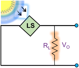
Recently, self-powered photodetectors have become a new area of interest for researchers in the photodetector domain. These photodetectors generate sufficient power on their own for the operation. Hence, they are known as self-powered photodetectors. The development of electric potential due to the photovoltaic effect results in the self-powered phenomenon.13 The primary objective of the self-powered photodetector is to generate sufficient power for the self-functioning of the photodetector. The working of a self-powered photodetector resembles the working of a solar cell operating in photovoltaic short circuit or open circuit mode14 but there is a fundamental difference between a self-powered photodetector and a solar cell. Solar cells are meant to absorb the maximum number of photons (irrespective of the photon's wavelength) and convert the same into electricity. In contrast, a self-powered photodetector absorbs photons of the intended wavelength only. The prospects for self-powered photodetectors not only depend upon the power generated by the detector but also on efficiently discriminating between the photons based on energy (or wavelength) given by the spectral selectivity of the detector. The photodetector is considered spectrum selective if the full-width at half-maxima (FWHM) of the detector is less than 100 nm.4 Self-powered photodetectors are further classified into two types: one generates sufficient power on its own15 and the second utilizes an energy harvesting unit.16 The energy harvesting unit fulfils the power requirement of the photodetector. Focusing on the abovementioned properties of self-powered photodetectors, there is a consistent issue found in the literature with self-powered photodetectors as broadband detectors. Regarding self-powered photodetectors, broadband detectors are closely correlated with the solar cell compared to photodetectors. Thus, this work primarily focuses on self-powered photodetectors, which are spectrum selective. A self-powered photodetector under illumination acts as a light-dependent voltage source (LS) as shown in Fig. 1 and provides sufficient power to trigger the externally dependent circuit or load.
Multiple good review articles are already available in the literature focusing on self-powered photodetectors. Tian et al.17 authored the first state-of-the-art review article on self-powered photodetectors. In this article, the prime focus was on junction engineering only; however, a broad device engineering view was missing. In an article by Ouyang et al.,18 self-powered photodetection was done only using ZnO nanomaterials, which in turn limited sensing to the UV region only. The article by Jayakrishnan19 discusses one of the latest techniques used in self-powered photodetection i.e. ferro-pyro-phototronics. However, there are other techniques that help in improving self-powered photodetector performance metrics like plasmonics, surface passivation and many others. Al Fattah et al.20 discussed UV light sensing only citing junction engineering. Perumal Veeramalai et al.21 focused only on the advantages of a perovskite in self-powered photodetection. The present work is focused on areas that are in general not covered by review articles including the relevance of noise studies for self-powered photodetectors, suitable device engineering techniques to minimize losses, and ways to improve the selectivity and figures of merit of self-powered photodetectors. Section 2 covers noise and performance parameters, followed by material specifications for self-powered photodetectors in section 3. Section 4 focuses on the crucial electric field factor, while section 5 explores the significance of ETLs and HTLs for photodetector performance. Lastly, sections 6–9 explore techniques for enhancing photodetector behaviour, including band-gap engineering, junction engineering, surface passivation, and additional effects.
2 Noise and performance parameters
2.1 Sources of noise
The information one can extract from the output of a photodetector is limited by its signal-to-noise ratio (SNR). The signal is the amount of incident photon energy while the noise is the disturbance that results in inaccurate measurement of the signal levels. In order to optimize the conclusion from the response, it is necessary to examine the sources of noise in the photodetector. The details of different sources of noise in the photodetectors are discussed below:• Shot noise: shot noise arises due to the statistically independent nature of photons arriving at the detector.22 Shot noise is a characteristic of a light source and cannot be eliminated with any technical device. Shot noise is a type of white noise (independent of frequency) and it is directly proportional to the intensity of incident light. The power spectral density of shot noise can be written as:
| σsh2 = 2qIph | (1) |
• Johnson noise (thermal noise): Johnson noise arises from temperature-dependent fluctuations in the load resistor (RL). It is also a type of white noise. Johnson noise can be represented with the help of a Gaussian distribution with power spectral density can be written as
 | (2) |
• Dark current noise: an ideal photodetector does not produce any current under dark conditions. However, due to thermal effects, there is still the probability of the spontaneous production of free electrons even in the absence of photons. The dark current has a fixed value at a particular temperature and it decreases with a decrease in temperature. Due to the statistical nature of the carrier generation process, the power spectral density of dark current noise can be written as:
| σd2 = 2qIdark | (3) |
The dark current noise and Johnson noise can be reduced by operating the photodetector at a lower temperature.
The other noises associated with photodetectors are flicker noise (1/f noise) and technical noise due to various imperfections. Noise-equivalent-power (NEP) is used to represent the noise power, which is equal to the minimum photon power required to overcome the noise current.23 It can be calculated from the responsivity per unit bandwidth.23,24
 | (4) |
The study of NEP provides many details about the noise sensitivity of the photodetector. Pal et al.23 studied the noise in a PbS quantum dot (QD)-based p–n junction photodiode. They showed that on increasing the biasing voltage, the EQE of the device increased at a particular wavelength and hence the NEP decreased. However, Lee et al.25 studied the effect of bias on flicker noise. They found that for a bandwidth of 1 kHz, the device (p-GaN/i-ZnO/n-ZnO:Al) exhibited NEPs of 5.56 × 10⁻¹² W and 2.93 × 10⁻¹² W for −5 V and −1 V respectively for 360 nm incident light. Therefore, flicker noise is less significant for self-powered photodetectors. Nawaz et al.26 fabricated a CdS nanobelt-based flexible self-powered photodetector. The detector exhibits a NEP of 2.94 × 10⁻¹⁵ W Hz−1/2. The ultra-low value of NEP is because the dark current of the device is 36 fA under zero-bias conditions. Similarly, Zhang et al.27 fabricated a broadband self-powered photodetector based on PdSe2. They calculated the thermal noise of the device. The thermal noise current is 7.61 × 10⁻¹⁴ A, which is much lower than the dark current (1.54 × 10⁻¹¹ A) of the device.
2.2 Performance parameters
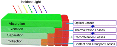
The concept/process of photodetection involves the following four steps as shown in Fig. 2:1. Optical absorption: it depends on the bandgap of the material and photon energy. Photons will be absorbed if the bandgap of the material is lower than the incident photon energy, otherwise, the semiconductor material (active material) will be transparent to the incident photons. The bandgap of the semiconductor material (Eg) should be lower than the photon energy (hν = hc/λ) to generate e–h pairs. The maximum wavelength (λ) that can generate e–h pairs can be written as:
 | (5) |
2. Charge excitation: the transfer of energy will happen between absorbed photons and the electrons. This process will excite electrons to the conduction band (higher energy levels), leaving holes in the valence band, thus called photogenerated charge carriers. The generated electrons and holes will undergo a Coulombic interaction and form an exciton. This leads to thermalization loss in which excited electrons and holes try to come to the edge of the conduction and valence band, respectively.
3. Charge separation and transportation: the charge carrier's separation is the movement of electrons and holes toward their respective terminals under the influence of the field. It also depends on the mobility of charge carriers and the carrier lifetime.28
4. Charge collection: the photodetection efficiency also depends upon external factors such as electrodes. The quality of the electrode will determine how much charge is collected from the active material.29
There are different losses associated with the photodetector at each stage starting from the incident photon until the flow of the output current as shown in Fig. 2. These losses are the combination of multiple issues, such as reflection or scattering of incident photons, recombination loss, transportation loss, and contact losses. For an n-type Si-based screen printed solar cell utilizing a polysilicon passivating contact, the resistive and recombination losses contribute to 63%.30 A bare Si solar cell causes about 30% of reflection losses.31 An ideal photodetector should have zero losses, and a practical photodetector varies from the ideal photodetector because of the above-mentioned losses only. The quality of a photodetector is dependent upon how much it is inclined towards the ideal photodetector as determined by the following figures of merit:
• Sensitivity: it represents the change in the output current when light is incident with respect to the current under dark conditions. It is the ratio of the photogenerated current (Iph) to the thermally generated current under dark conditions (Idark).32
 | (6) |
High sensitivity is an essential requirement for any photodetection application such as medical diagnosis, optical communication, and many others.
• Rise time and fall time (s): rise time and fall time define the rate at which the photodetector generates output with respect to the change in input conditions (illumination). In general, the rise time is the time taken for the output to change from 10% to 90% of the final value while the fall time is the time taken for the output to change from 90% to 10% of the initial value.33 The rise time and fall time are of great importance in various applications such as optical communication, optical storage, LiDAR, time-resolved spectroscopy, and terahertz imaging. Detectors with a superior rise time are generally treated as ultrafast photodetectors, thus rise time represents the speed of the photodetector.
• Responsivity (A W−1): the response of the device in terms of output current to input photon flux (optical power intensity) gives the responsivity.32 This figure of merit directly correlates the system's input with the system's output and thus can be seen as the transfer function of the photodetector. A prerequisite for applications like fibre-optic communication, astronomical observation, and medical diagnosis is the high responsivity of the photodetectors.
 | (7) |
• External quantum efficiency (%): the chain effect that leads to the sensing mechanism of photodetectors starts with decreasing the phonon flux. The generated electron–hole (e–h) pair with respect to incident photon flux density gives the photodetector's internal quantum efficiency (IQE). The generated e–h pairs are expected to be extracted via an external circuit leading to current flow in the circuit, but this process also loses charge pairs due to recombination and trap states. This loss is accommodated with an external quantum efficiency (EQE) which gives the ratio of the number of e–h pairs collected at the terminals with respect to the number of incident photons.34 The maximum EQE one can achieve is equal to the IQE, thus representing the device's photogeneration, extraction, and collection efficiency. High efficiency is desired for every application where a photodetector is required.
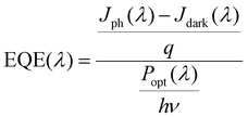 | (8) |
Finally using eqn (7) with eqn (8), we can write:
 | (9) |
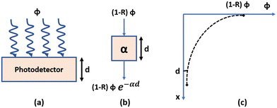
The EQE of a detector depends on the photon flux (ϕ) and the reflectivity (R).35 Assuming the detector thickness is d as shown in Fig. 3(a), then ϕ(1 − R) amount of flux will enter the detector material. The ϕ(1 − R) amount of flux, will go through the absorption in the detector's material depending upon the absorption coefficient (α) as shown in Fig. 3(b) and (c).
| Absorbed energy = ϕ(1 − R)(1 − e−αd) | (10) |
| n = ϕ(1 − R)(1 − e−αd)ζ | (11) |
 | (12) |
The EQE of the detector can be maximized by tuning R, αd, and ζ as discussed below:
- The reflection can be minimized by utilizing an anti-reflection coating (ARC). The ARC is made for a particular wavelength only.
- By making αd large. This will decrease the e−αd term and thus increase the EQE.
- ζ can be minimized by meticulous fabrication of the detector material. Improvement in ζ can be observed by minimizing defects and also utilizing charge transport layers for faster extraction.36,37
• Detectivity (Jones or cm Hz1/2W−1): the detectivity of a photodetector is the minimum number of photons (photon flux density) required to generate the current in the external circuit.38 The output current is impacted by the device's internal current (thermal current). The detectivity of a photodetector is inversely proportional to the noise-equivalent power (NEP). Thus, the detectivity decreases with an increase in noise current. Applications like medical diagnosis and astronomical observations require very high detectivity.
 | (13) |
• Spectral selectivity: the importance of a photodetector is observed from its discriminating behaviour between photons of different energies. This behaviour is generally classified using spectral selectivity, which depends upon the effective response width given as the FWHM.12 This criterion is important for all applications that require precise detection of the photon energy.
The losses associated with a photodetector are undesirable and limit the performance of a photodetector. By utilizing suitable device engineering techniques, these losses can be minimized to a certain extent and hence there will be obvious improvement in the figures of merit. In other words, device engineering in self-powered photodetectors revolves around optimizing the performance parameters. This includes enhancing light absorption, charge carrier generation, and extraction, and minimizing losses due to recombination and resistance. So, engineers can work on the materials, interfaces, and device architectures to achieve these goals.
3 Material specifications
The specifications of materials for self-powered photodetectors depend on the application and desired performance characteristics. However, the general considerations for materials are as follows:• Bandgap: the bandgap of the material should match the wavelength of the light and should be less than or equal to the energy of the photon for e–h pair generation. For example, the energy brought by the red light (720 nm) photon is 1.72 eV while the energy brought by the violet light (400 nm) photon is 3.1 eV.
• Mobility: the mobility of the charge carriers in the semiconductor material should be very high. It has an impact on the speed and ability to detect weak signals. However, a higher mobility results in a higher dark current, but the dark current can be minimized by utilizing junction engineering.39
• Stability: under various operating conditions such as moisture, heat, and exposure to light, the semiconductor's electrical and optical properties should remain stable.
• Cost: the cost of the material should be as low as possible. It is a very important parameter for large-scale applications.
The different materials utilized nowadays for self-powered photodetectors are:
Wide bandgap semiconductors:40,41 these materials have large bandgaps and are suitable for ultraviolet and visible light detection. Some of the examples are ZnO, GaN, InP, and SiC.
0D, 1D, and 2D materials:42,43 these materials have a high surface-to-volume ratio, which can make them more sensitive to light than traditional bulk semiconductors.44
As research into self-powered photodetectors continues, new materials and device architectures are being explored. This is leading to the development of more efficient, sensitive, and versatile self-powered photodetectors for a variety of applications.
4 Origin of the electrical field
For photodetectors to function appropriately, it is necessary to carry out two essential processes: the separation and collection of photogenerated charge carriers through electrodes. The effectiveness of charge carrier separation depends on the electric field that is established across the depletion region. On the other hand, several factors, including but not limited to an electric field, carrier transit time, trap states, and carrier mobility, influence the collection ratio.46 It is worth noting that the electric field, which can be either internal or externally enhanced, is the driving force for separating and collecting charge carriers. External sources, such as batteries, are typically used to provide the electric field in conventional photodiodes. Recent research has focused on replacing external battery sources with photovoltaic units and piezo-nanogenerators to develop self-powered photodetector assemblies as a potential replacement for traditional photodetectors.16,47–49 Xu et al.47 successfully demonstrated that the lateral integration of 700 rows of ZnO nanowires (NWs) could generate 1.26 V when subjected to a strain of 0.19%. This system was utilized to power the UV sensing capabilities of ZnO NWs. Bie et al.45 fabricated a self-powered photodetector that incorporated an energy harvesting unit. This device features a CdSe NW that is powered by an n-ZnO/p-GaN photovoltaic unit, as illustrated in Fig. 4. The device demonstrates exceptional transient response, with a rise time of 20 μs and a fall time of 219 μs. Additionally, it functions as an optical AND gate for both red and UV light. In their work, Wu et al.48 employed a flexible piezo-nanogenerator as the power-generating unit. They developed a self-powered photodetector utilizing a PZT NW textile nanogenerator, with the UV sensing element comprising ZnO NWs. The nanogenerator is capable of producing a maximum output voltage of 240 mV and a current of 2.5 nA. The voltage drop across the UV sensing unit can be utilized to estimate the level of light intensity. As the UV intensity increases, the generation of charge carriers also increases, leading to a reduction in resistance and a voltage drop across the UV sensing unit. Apart from the photovoltaic unit and piezo-nanogenerator, micro-supercapacitors have also been utilized as an energy harvesting unit by researchers. A flexible photodetector with micro-supercapacitors integrated on a chip was developed by Xu et al.49 The photodetector comprises CdS NWs, while the micro-supercapacitor is made from reduced graphene oxide (rGO).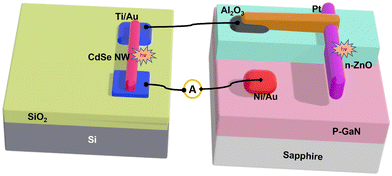 | ||
| Fig. 4 Schematic of a CdSe NW-based photodetector utilizing a ZnO/GaN-based energy harvesting unit.45 | ||
Lu et al.16 developed a nanosystem consisting of a photodetector and a solar cell-based energy harvesting unit. The system utilized a perovskite-based (CH3NH3PbI3) solar cell to power the perovskite-based photodetector, as illustrated in Fig. 5. The integration-based systems, where external energy harvesting units are coupled with photodetectors, can provide excellent electrical and optical properties, but they lack the flexibility to be easily integrated into an integrated circuit due to their increased size or complex design. Thus, interest in compact systems that rely on utilizing the internal field for charge carrier extraction is increasing and these systems show potential for application in the development of next-generation nanoscale integrated self-powered photodetectors.
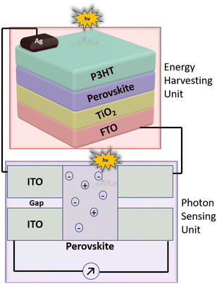 | ||
| Fig. 5 Schematic of a photodetector-solar cell-based nanosystem.16 | ||
The following study delves into the topic of self-powered photodetectors, which are capable of generating power independently without the need for any external energy harvesting unit. The performance of these devices depends on several factors, including the materials utilized, the type of junction formed, the type of electrode used, and the incorporation of various effects. Each of these performance enhancement factors is discussed in detail in the following sections.
5 Utilization of ETLs and HTLs
The photogenerated carriers must be separated and collected before they recombine for the proper functioning of a photodetector.50 However, materials with a low carrier lifetime suffer from the issue of early charge carrier recombination, which necessitates device engineering techniques to collect the photogenerated charge carriers effectively. Utilizing the electron-transport-layer (ETL) and hole-transport-layer (HTL) can significantly improve the collection of photogenerated carriers in low-carrier lifetime materials. The ETL and HTL refer to the highly doped n-type and p-type semiconductor layers respectively. They are crucial in creating an electric field that drives the charge carriers toward the respective terminals, thus preventing recombination. The formation of the depletion region enables the ETL to attract electrons, while the HTL attracts holes and repels charges of opposite polarity.Fig. 6(a) depicts a photodetector that employs an ETL and an HTL. Light enters from the FTO/ITO side, which serves as a transparent conductor, resulting in 100% illumination area. The band diagram is shown in Fig. 6(b), illustrating that the ETL and HTL assist in moving electrons and holes toward the cathode and anode, respectively. As a result, the probability of charge carrier recombination is reduced. Improved carrier extraction results in enhanced figures of merit of the self-powered photodetector, such as response time, sensitivity, detectivity, responsivity, and EQE. Xie et al.51 fabricated a blue light hybrid self-powered photodetector. The device employs a hybrid heterojunction between an n-TiO2 nanorod array (NRA), an inorganic material, and a p-spiro-MeOTAD, an organic material, where TiO2 act as an ETL and spiro-MeOTAD act as the active layer and HTL. The photodetector exhibits a rapid response with a rise time of 120 ms and a fall time of 60 ms. Kumar et al.52 also developed a self-powered photodetector with an ETL-only architecture. This photodetector is believed to be the first to be based on quantum dots (QDs). The device forms a Schottky junction between Au electrodes and CdSe QDs, with CdSe being the active layer. The ETL, consisting of ZnO QDs, enables efficient electron extraction. The device exhibited an excellent transient response, with a rise-time of 17.9 ms and a fall-time of 18 ms. Goel and Kumar53 improved upon the device built by Kumar et al.52 by introducing an HTL layer made of MoOx and incorporating a transparent ITO electrode. They utilized MoOx along with ZnO QDs and CdSe QDs in the device. They observed a 15% improvement in key performance metrics such as rise time, responsivity, detectivity, and EQE compared to the device without the HTL. Shen et al.54 achieved an even better transient response by incorporating TiO2 and spiro-MeOTAD layers as the ETL and HTL, respectively, in their self-powered photodetector. The device was fabricated on a flexible ITO/PET substrate and the perovskite QDs (CsPbBr3) were utilized as the active layer. The resulting device exhibited an extremely fast transient response, with a rise time of only 2.3 ms. Zhou et al.55 demonstrated that the doping of charge transport layers could also enhance the performance of self-powered photodetectors. They55 fabricated a visible self-powered photodetector using Ga-doped ZnO nanorods (NRs) and the MAPBI3 perovskite as an active layer. The Ga-doped ZnO NRs were utilized as the ETL, and the device exhibited an ultrafast transient response with a rise/fall time of 2 ms.
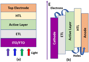 | ||
| Fig. 6 (a) Schematic of a photodetector with back illumination utilizing an ETL and an HTL, (b) energy band diagram of the photodetector. | ||
According to Li et al.,56 various materials can be used as the HTL and ETL in self-powered photodetectors, including TFB, TIPS pentacene, PEDOT:PSS, NiOx, MoOx, V2O5, CuSCN, BCP, Bphen, C60, PEIE, PFN, PEI, ZnO, TiO2, SnO2, Cs2CO3, and others. An HTL layer is crucial for the organic material-based active layer, as without it, there would be little to no response. TiO2 and ZnO are commonly used ETLs due to their excellent hole-blocking property and transparency to solar radiation. Voroshazi et al.57 conducted a stability analysis of various ETLs and HTLs, finding that ZnO and TiO2 have better stability than other organic ETLs. Regarding HTLs, they compared the performance of MoO3 and PEDOT:PSS, and surprisingly, found that PEDOT:PSS-based devices had higher stability than MoO3-based devices. The MoO3-based device showed a stability of approximately 4000 h, while the PEDOT:PSS-based device showed a stability of approximately 5000 h. Similarly, Jarwal et al.36 investigated the impact of seven different organic HTLs on the performance of the perovskite-based solar cells. After conducting an extensive study, they discovered that using spiro-OMeTAD as an HTL led to better performance metrics than the other six organic HTLs, which were PTAA, PQT, P3HT, MEH-PPV, nPB, and PEDOT:PSS.
This section states that the device engineer should select the ETL and HTL wisely before fabricating the self-powered photodetector since the ETL and HTL are essential for organic materials since organic materials suffer from lower mobility and the utilization of the ETL and HTL facilitates the movement of charge carriers towards their respective terminals, resulting in improved figures of merit.
6 Bandgap engineering
Bandgap engineering involves adjusting the bandgap of a material to optimize its electronic and optical characteristics for a specific purpose. In the context of a photodetector, bandgap engineering can enhance its performance and spectral coverage. By doing so, light absorption can be improved, leading to better figures of merit. In general, the bandgap is modified using the following techniques:6.1 Quantum confinement
The process involves constructing a structure with dimensions comparable to the Bohr radius or the electron's wavelength, such as a quantum dot, nanowire, or nanosheet, which results in modifications to the material's electronic properties as a function of particle size. The specific form of quantum confinement gives rise to various material types, as described below44,58 and shown in Fig. 7.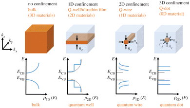 | ||
| Fig. 7 Types of materials based on confinement.58 Published with “Royal Society Open Science” as open access, 2018. | ||
• 3-D materials (no confinement): electrons can move in all three dimensions, also known as bulk materials.
• 2-D materials (1-D confinement): 2-D materials refer to materials that permit unrestricted electron motion in two dimensions while restricting it in one dimension, commonly referred to as quantum sheets or quantum wells.
• 1-D materials (2-D confinement): in 1-D materials, electrons can move freely along one direction while their motion is restricted in the other two dimensions, commonly called nanowires.
• 0-D materials (3-D confinement): in 0-D materials, such as quantum dots (QDs), the motion of electrons is restricted in all three dimensions. The constrained structure of QDs results in unique charge transport behaviour compared to other dimensional materials (1-D, 2-D, and 3-D). In QDs, the primary charge transport mechanism is through the tunneling and hopping of charge carriers.60
Due to quantum confinement, the bandgap of a material increases as the particle size decreases. CdSe nanoparticles of varying sizes were synthesized by Murray et al.,61 and they found that the bandgap decreased (from 2.4 to 1.7 eV) with an increase in particle size (from 2 to 20 nm). Kumar et al.59 also demonstrated the effect of quantum dot size on the photodetector response by using a heating technique to change the size of ZnO QDs during annealing. As shown in Fig. 8, they obtained bandgaps of 3.42, 3.26, and 3.23 eV for sizes of 4.42, 8.74, and 13.89 nm, respectively. The relationship between the bandgap of a QD as a function of its particle size (radius of QD, R) and its bulk counterpart can be described by the following equation, according to Murphy et al.:62
 | (14) |
 | (15) |
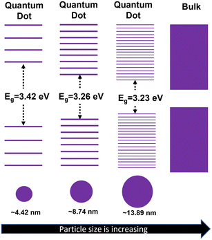 | ||
| Fig. 8 Demonstration of variation of the bandgap of quantum dots (QDs) with respect to the size of the QDs.59 | ||
The carrier mobility in the equation is denoted as μ(E) and the electric field-dependent hopping rate as R(E), while d represents the distance to the nearest hopping neighbour. Gilmore et al.63 modeled the hopping rate as a function of the relative positions and energetics of nearby QDs as indicated in eqn (16). They utilized the Miller–Abrahams rate equation to describe the hopping rate of an electron from the ith QD to the jth QD in the conduction band.
 | (16) |
6.2 Doping and alloying
Alloying and doping are two common techniques for modifying material properties. Alloying involves mixing two or more elements to form a new material with different properties, while doping introduces impurities into a material to modify its electrical and optical properties. The main difference is that alloying changes the material's crystal structure,69 whereas doping does not alter the crystal structure but changes its electrical and optical properties.70 Boruah et al.64 investigated the effect of doping on photocurrent in a ZnO NRA. The nanorods were doped with F, Cl, Br, and I, and the device was based on an ITO/doped:ZnO NR/PEDOT:PSS/Ag UV photodetector. The Cl-doped ZnO-based device exhibited enhanced figures of merit with a sheet charge density of 7 × 1010 cm−2 and a photocurrent of 220 nA. The sheet charge densities and corresponding photocurrents for doped ZnO nanorods are listed in Table 1. The results of photoluminescence analysis demonstrate a blueshift in the bandgap of ZnO NRs due to doping. Abbasi et al.65 investigated the impact of varying levels of Cd doping in ZnO NRs, ranging from 0% to 7%. They calculated various parameters to study the optical behaviour of the devices, as listed in Table 2. The highest sensitivity, responsivity, and detectivity were obtained with 7% Cd doping, while the fastest response was achieved with 5% Cd doping. The bandgap remained consistent with doping, but the photoluminescence intensity increased, indicating a higher number of direct generation and recombination events suitable for photodetection applications. Kumar et al.66 also examined the effect of Al and Mg doping of CdS and determined the resulting devices’ optical parameters, such as responsivity, detectivity, and EQE. They discovered that the material's bandgap varied depending on the dopant, ranging from 2.3 eV to 2.25 eV. The extracted device parameters are presented in Table 3. The study concludes that doping with various materials can shift the bandgap, while varying the doping concentration can directly influence the charge generation and recombination mechanisms.| S. no | Photodetector | Sheet charge density (cm−2) | Photocurrent (nA) |
|---|---|---|---|
| 1 | ZnO NRs | 0.323 × 10¹⁰ | 40 |
| 2 | F:ZnO NRs | 4.62 × 10¹⁰ | 150 |
| 3 | Cl:ZnO NRs | 7 × 10¹⁰ | 220 |
| 4 | Br:ZnO NRs | 3.8 × 10¹⁰ | 140 |
| 5 | I:ZnO NRs | 0.92 × 10¹⁰ | 90 |
| Sample (Cd%) | Avg. diameter (nm) | Avg. length (nm) | Photocurrent (nA) | Rise time (s) | Decay time (s) | Sensitivity (Iph/Id) | Responsivity (μA W−1) | Detectivity (Jones) |
|---|---|---|---|---|---|---|---|---|
| 0% | 50–60 | 300–400 | 32.08 | 18 | 13 | 110.62 | 2.07 | 0.22 × 10⁹ |
| 3% | 50–70 | 500–650 | 162.15 | 8 | 10 | 463.28 | 10.46 | 0.98 × 10⁹ |
| 5% | 40–60 | 600–700 | 320.21 | 2.5 | 4 | 762.40 | 20.66 | 1.8 × 10⁹ |
| 7% | 60–75 | 850–1000 | 460.10 | 5 | 6 | 920.30 | 29.68 | 2.4 × 10⁹ |
| Thin film materials | Rise time (ms) | Decay time (ms) | EQE (%) | Responsivity (A W−1) | Detectivity (Jones) |
|---|---|---|---|---|---|
| CdS | 840 | 910 | 41.36 | 0.17 | 7.12 × 10¹⁰ |
| CdS:Mg (3%) | 780 | 880 | 327.46 | 1.40 | 4.05 × 10¹¹ |
| CdS:Al (3%) | 750 | 850 | 497.29 | 2.13 | 5.23 × 10¹¹ |
| CdS:Mg (3%) & Al (3%) | 820 | 890 | 72.50 | 0.31 | 1.43 × 10¹¹ |
Researchers have also tried to modify the bandgaps of the materials by alloying as the alloyed material has more tolerance to lattice mismatch and can be utilized to tailor the electronic and optical properties of the photonic devices.71 Hao et al.71 employed alloy engineering to tailor the bandgap and observed a decrease in the bandgap of InSe1−xTex with an increase in ‘x’ values. Conversely, the bandgap of InSe1−xSx increased with increasing ‘x’. For a constant value of x = 0.2, the bandgap of InSe0.8Te0.2 is found to be 1.11 eV, while that of InSe0.8S0.2 is 1.34 eV. In a similar approach, VK and Rao also investigated the effect of varying the value of ‘x’ on the bandgap of CdxZn1−xS. The value of ‘x’ was determined using EDAX analysis, and the bandgap was obtained using the Tauc relation (eqn (17)) from UV-Vis spectrophotometry. Their findings indicate that the material's bandgap decreases as ‘x’ increases.
| αhν = A(hν − Eg)n | (17) |
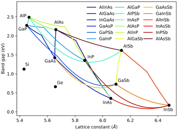 | ||
| Fig. 9 Variation of bandgap with lattice constant in different alloyed materials,67 Published by “Springer Nature” as open access, 2018. | ||
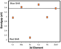 | ||
| Fig. 10 Variation in bandgap with respect to dopants for the host ZnO.68 | ||
![[thin space (1/6-em)]](https://www.rsc.org/images/entities/char_2009.gif) 73
73
| S. no | Sample | Bandgap (eV) |
|---|---|---|
| 1 | Pure ZnS | 4.2 |
| 2 | Sn0.02Zn0.98S | 4.14 |
| 3 | Sn0.04Zn0.96S | 4.10 |
| 4 | Sn0.06Zn0.94S | 3.99 |
| 5 | Sn0.08Zn0.92S | 3.91 |
| 6 | Sn0.1Zn0.9S | 3.87 |
| 7 | Sn0.12Zn0.88S | 3.83 |
6.3 Superlattice
A superlattice is a structure that involves the layering of multiple materials with different bandgaps, resulting in a combined bandgap determined by the thickness and bandgap of each material.75 Researchers have utilized superlattice structures in the development of various photodetectors. For instance, Li et al.76 developed a transparent UV photodetector using an InGaZnO-based superlattice structure with a responsivity of 64![[thin space (1/6-em)]](https://www.rsc.org/images/entities/char_2009.gif) 600 A W−1 at −20 V. Similarly, Delli et al.74 fabricated a mid-infrared InAs/InAsSb superlattice photodetector as shown in Fig. 11 with an EQE of 25.6% at 200 K and a maximum specific detectivity of 3.65 × 10¹⁰ Jones with top illumination at 100 mV, although no significant work has been reported for self-powered photodetectors utilizing a superlattice structure.
600 A W−1 at −20 V. Similarly, Delli et al.74 fabricated a mid-infrared InAs/InAsSb superlattice photodetector as shown in Fig. 11 with an EQE of 25.6% at 200 K and a maximum specific detectivity of 3.65 × 10¹⁰ Jones with top illumination at 100 mV, although no significant work has been reported for self-powered photodetectors utilizing a superlattice structure.
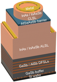 | ||
| Fig. 11 Schematic of the InAs/InAsSb type-II superlattice structure grown on GaSb/AlSb/Si buffer, using AlSb/GaSb dislocation filters.74 Published with “American Chemical Society” as open access, 2019. | ||
In summary, the bandgap is a critical parameter for determining the absorption characteristics and current output of a self-powered photodetector. Engineers carefully select semiconductor materials with appropriate bandgaps to achieve optimal energy conversion efficiency in photodetector designs.
7 Junction engineering
In self-powered photodetectors, the photogenerated charge carriers should be separated and collected at the respective electrodes before they recombine. This separation and collection are governed by the built-in electric field.17,77 The built-in field is provided by the different junctions formed like homojunctions, heterojunctions, and Schottky junctions. The operational mechanisms of various self-powered photodetectors are demonstrated in Fig. 12. The photogenerated charge carriers are separated by an electric field set up by the immobile ions or fixed charges in the depletion region.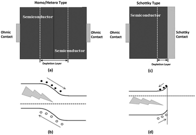 | ||
| Fig. 12 (a) Schematic and (b) band diagram of homo/heterojunction-based self-powered photodetectors. (c) Schematic and (d) band diagram of Schottky junction-based self-powered photodetectors. | ||
7.1 Junction between semiconductors (homo/heterojunction)
The homojunction is the most commonly used type of junction, which utilizes the same kind of semiconductors. Shen et al.78 fabricated a device using the n-ZnO/p-ZnO:(Li,N) homojunction. The fabricated detector shows an FWHM of 9 nm due to the filtering action of undepleted p-ZnO (doped). They78 showed that increasing the bias voltage led to an increment in the depletion region and a reduction in the FWHM. Another frequently employed technique to create efficient self-powered photodetectors is using heterojunctions, which involve materials with varying bandgaps.79 This process involves the epitaxial growth of different layers, making heterojunctions easy to fabricate. Depending on the types of semiconductors forming the junction, heterojunctions can be classified into two categories. Isotype heterojunctions are formed when the junction is between semiconductors of the same type (p–p or n–n). In contrast, anisotype heterojunctions are formed when the junction is between semiconductors of different types (p–n). Hassan et al.80 fabricated a self-powered photodetector using p-Si and n-ZnO NRs (anisotype heterojunction). This device demonstrated a response time of 25 ms and a recovery time of 22 ms, with a sensitivity of approximately 8000% under UV illumination.Hybrid heterojunctions, which combine the benefits of both organic and inorganic semiconductors, have been explored by researchers. This type of junction offers the low-cost and environmentally friendly advantages of organic semiconductors and the high carrier mobility of inorganic semiconductors.81 For instance, Kumar et al.82 developed a self-powered photodetector using CdSe QDs and PQT-12 hybrid heterojunctions. The device has a spectral peak at approximately 420 nm and a rise and fall time of 15.32 and 12.01 ms, respectively. Li et al.83 developed a self-powered photodetector based on CdSe and p-Sb2 (S1−xSex)3, as illustrated in Fig. 13(a). The photogenerated electrons move toward FTO while holes move toward spiro-OMeTAD, as shown in Fig. 13(b). The device covers a spectral range from 650 nm to 900 nm. By varying the CdSe thicknesses and Se concentration, the researchers achieved selectivity, as shown in Fig. 13(c) and (d), respectively.
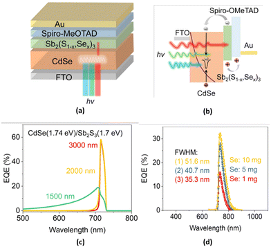 | ||
| Fig. 13 (a) Schematic of the self-powered photodetector, (b) schematic of carrier transport in the device, (c) EQE for different CdSe thicknesses, and (d) EQE for different Se concentrations.83 Published by “Wiley-VCH” as open access, 2021. | ||
7.2 Junction between a metal and a semiconductor (Schottky junction)
The interface between a metal and semiconductor can exhibit three distinct behaviours: ohmic, tunneling, and Schottky junctions.50 In the case of ohmic and tunneling contacts, charge carriers can flow freely without encountering any barriers, and thus these contacts serve purely as a means of connection. On the other hand, Schottky junctions provide a rectifying barrier that responds to bias and features a depletion region that extends primarily toward the semiconductor. It is important to consider the metal and semiconductor's work function to ensure the formation of an efficient Schottky junction. When forming a junction between an n-type semiconductor and metal, the metal's work function should be greater than the semiconductor's. Conversely, for a p-type semiconductor and a metal junction, the semiconductor's work function should be greater than the metal's. Nonetheless, it is worth noting that the minimum criteria for forming a Schottky junction involve the metal's work function and the semiconductor's electron affinity.50 Devices based on Schottky junctions are known to be more sensitive and faster than those based on two-ohmic contacts. The metal used for Schottky contacts can include graphene, Au, Ag, and others. Graphene, being a 2D material with high mobility, is a promising candidate for self-powered photodetectors. Jin et al.109 utilized graphene in a Schottky contact with a CdSe nanobelt to create a self-powered photodetector with high photosensitivity. The fabricated device shows a photosensitivity of ∼3.5 × 10⁵ and a fast transient response time, with a rise and fall time of 82 and 179 μs, respectively. A Schottky junction between graphene and a CdSe nanobelt was also fabricated by Gao et al.110 This structure was implemented on a flexible substrate, and the researchers achieved better transient times with a rise and fall time of 70 and 137 μs, respectively. However, the study did not investigate whether the photodetector's response was affected by the rolling or bending of the flexible substrate. Duan et al.85 developed a self-powered photodetector using a graphene-based Schottky contact in conjunction with a ZnO:Al NRA and found an improved rise time and responsivity of 37 μs and 39 mA W−1, respectively. Benyahia et al.89 developed a self-powered photodetector utilizing Au as a Schottky contact with a ZnO–ZnS active layer prepared at 500 °C. The detector exhibits a response across a broad spectral range of 300 to 900 nm but cannot efficiently discriminate photons, a crucial property of photodetectors. Purusothaman et al.90 developed a self-powered photodetector utilizing a floral-like ZnO NR structure with an Ag-based Schottky contact. The device was fabricated on a flexible PVDF substrate, demonstrating a responsivity of 22.76 mA W−1. In the field of research, Schottky junction-based devices are often preferred over homojunction and heterojunction-based devices due to their faster transient times and ease of fabrication.111 A list of different self-powered photodetectors categorized based on junction engineering can be found in Table 5.| Structure materials | Structure category | Response (recovery) time | Responsivity (mA W−1) | Detectivity (Jones) | EQE (%) | Spectrum region | FWHM (nm) |
|---|---|---|---|---|---|---|---|
| Graphene/ZnO NW/graphene84 | Schottky | — | ∼0.55 | — | 0.185 | UV | ∼100 |
| Graphene/ZnO:Al NRA-film85 | Schottky | 37 (330) μs | 39 | — | — | UV | <100 |
| Graphene/H2O2-treated ZnO86 | Schottky | 32 ms | 0.050 | — | — | UV | — |
| Au-ZnO-Au MSM structure87 | Schottky | — | 20 | — | — | UV | ∼100 |
Au/ZnO/GaN/Al2O3![[thin space (1/6-em)]](https://www.rsc.org/images/entities/char_2009.gif) 88 88 |
Schottky anisotype heterojunction | 731 (53.1) ms | 95.8 | 2.9 × 10¹² | — | UV | <100 |
| Au-SnxZn1−xS-Au MSM73 | Schottky | — | 47.1 | 1.64 × 10⁹ | — | UV | — |
| Au/ZnO–ZnS microstructured composite/Au MSM89 | Schottky | 22.5 (45.2) ms | 3.34 | 8.9 × 10¹² | — | UV–visible–NIR | >100 |
| 22.3 (40.1) ms | 1.05 | 2.8 × 10¹² | |||||
| 25.2 (15.6) ms | 0.47 | 1.4 × 10¹² | |||||
| Floral-like F-ZnO NRs on PVDF90 | Schottky | — | 22.76 | 2.72 × 10¹⁰ | — | UV | — |
| Se/In–Ga microrod91 | Schottky | 124 (146) μs | 408 | 1.30 × 10¹³ | — | UV-visible | >100 |
| Au/CdSe QDs/ZnO QDs/n-Si52 | Schottky isotype heterojunction | 17.9 (18) ms | 10.23 | 8.81 × 10⁹ | — | UV | >100 |
| Pd(Au)/CdSe QDs/ZnO QDs/ITO92 | Schottky isotype heterojunction | 17.15 (28.9) ms | 7.48 (2.7) | 1.3 × 10¹⁰ (8 × 10⁹) | 2.21% (0.87%) | — | ∼61 (190) |
| ZnO/GaN45 | Anisotype heterojunction | 20 (219) μ s | — | — | — | UV | <100 |
| ZnO NRA/p-Si80 | Anisotype heterojunction | 25 (22) ms | — | — | — | UV | — |
| ZnO NR/p-CuSCN93 | Anisotype heterojunction | 0.5 (6.7) μ s | 7.5 | — | — | UV | <100 |
| ZnO NR/p-CuSCN94 | Anisotype heterojunction | ∼25 ns (4 ms) | 50 | — | — | UV | <100 |
| ZnO NW array/graphene/CdS/electrolyte95 | Heterojunction | 5 ms | 27.3, 4.3 | — | — | UV, Visible | <100 |
| ZIF-8@H:ZnO NRs/p-Si96 | Anisotype heterojunction | 252 (607) μ s | 7070 | 2.14 × 10¹⁶ | — | UV-NIR | >100 |
| ZnO–Co3O4 nanowire97 | Anisotype heterojunction | 6 s | 21.80 | 4.12 × 10¹² | — | Visible | — |
| CuI/In–Ga–Zn–O40 | Anisotype heterojunction | 2.5 (35) ms | 0.6 | — | UV | — | |
| Carbon dot enhanced ZnO/graphite98 | Heterojunction | 2 (∼3.2) s | 9.57 | 4.27 × 10⁸ | — | UV | — |
Cu2ZnSnS4 (CZTS) and MoS2![[thin space (1/6-em)]](https://www.rsc.org/images/entities/char_2009.gif) 99 99 |
Anisotype heterojunction | 81 (79) ms | 141 | — | — | — | — |
| InGaZnO/p-silicon NW100 | Anisotype heterojunction | ∼0.1 ms | 530 | — | — | UV | >100 |
| p-NiO/n-Si101 | Anisotype heterojunction | <85 ms | 13.08, 46.02, 44.49 | 1.03 × 10¹¹, 3.65 × 10¹¹, 3.53 × 10¹¹ | 4.43, 8.62, 6.47 | UV, red, NIR | — |
| CuI/CsCu2I3/GaN102 | Anisotype heterojunction | 8.8 (0.32) s | 71.7 | 3.3 × 10¹² | 26.1 | UV | <100 |
FTO/ZnO/perovskite + GaZnO NRs/MoO3![[thin space (1/6-em)]](https://www.rsc.org/images/entities/char_2009.gif) 55 55 |
Anisotype heterojunction | <2 ms | 300 | 1.3 × 10¹² | — | UV | >100 |
| ZnO NWs/p-Si with Ga doping103 | Anisotype heterojunction | 1.4 (1.1) s | 192 | 1.09 × 10¹³ | 62.7 | UV | <100 |
SnS2/ZnO1−xSx![[thin space (1/6-em)]](https://www.rsc.org/images/entities/char_2009.gif) 104 104 |
Anisotype heterojunction | 49.51 (25.93) ms | 8.28 | 5.09 × 10¹⁰ | — | UV to NIR | <100 |
| N:ZnO-SpiroMeOTAD105 | Hybrid anisotype heterojunction | 200 (950) μ s | 17 | — | — | — | >100 |
| ZnO@CdS core–shell nanorod arrays106 | Anisotype heterojunction | 20 ms | — | — | — | UV, visible | — |
CdSe QD/PQT-12![[thin space (1/6-em)]](https://www.rsc.org/images/entities/char_2009.gif) 82 82 |
Hybrid anisotype heterojunction | ∼12.01 (∼15.32) ms | 3.3 | 5.4 × 10⁹ | — | Visible | >100 |
| p-ZnO:(Li,N)/n-ZnO78 | Homojunction | — | ∼0.016 | — | — | UV | 9 |
| Au-MgZnO-Au107 | Schottky | 0.23 (92) μs | 2.22 | 4.4 × 10¹¹ | — | UV | <100 |
| n-NiO nanoflakes/AZO NRs108 | Isotype heterojunction | ∼2 ms | 85.12 | 1.74 × 10¹² | — | UV | 9 |
| FTO/CdSe/Sb2(S1−x,Sex)3/spiro-OMeTAD/Au83 | Hybrid anisotype heterojunction | — | 190 | — | 32.2 | NIR | 35.3 |
| ITO/ZnO QDs/CdSe QDs/MoOx/Pd53 | Schottky aniso + iso type heterojunction | 13.56 (26.56) ms | 11.8 | 1.74 × 10¹⁰ | 3.73 | Violet-indigo | 67 |
In summary, junction engineering in self-powered photodetectors focuses on creating favourable conditions for efficient charge separation, minimizing recombination losses, and optimizing band alignment, facilitating effective charge transfer between different semiconductor layers. These efforts contribute to improving the overall performance and efficiency of self-powered photodetectors.
8 Surface passivation
At the surface of a semiconductor, atoms at the surface lack a bonding neighbour and this results in dangling bonds. These dangling bonds introduce a forbidden energy gap that charge carriers can use as recombination sites. Surface passivation is a technique used to improve the efficiency of detectors by creating a protective layer on their surface that reduces the number of defects and population of minority carriers. Thin films of a semiconductor material such as silicon nitride, SiNx (for n-type surfaces), or aluminium oxide, AlOx (for p-type surfaces), are grown on the detector's surface using chemical vapour deposition or atomic layer deposition techniques. These passivation layers reduce the recombination of electrons and holes, thereby improving the detector's overall response.113Zeng et al.112 fabricated a NIR self-powered photodetector using a graphene/Si nanotube array as shown in Fig. 14. In addition, surface passivation with methyl termination (–CH3) is used to enhance the detector's figures of merit. With –CH3 passivation, the device's sensitivity, responsivity, and detectivity are found to be 107, 0.328 A W−1, and 6.03 × 10¹³ Jones, respectively, which are much higher than the figures of merit of the device without surface passivation.
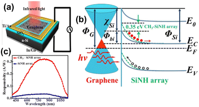 | ||
| Fig. 14 (a) Schematic of a graphene/Si nanohole array Schottky junction based self-powered near-infrared photodetector, (b) energy band diagram of the device with and without surface passivation under light, and (c) responsivity with and without surface passivation for different wavelengths.112 Published with “Optica Publishing Group” as open access, 2015. | ||
In summary, surface passivation in self-powered photodetectors is essential for reducing surface recombination, improving carrier lifetimes, and enhancing the overall performance.
9 Integrating additional effects
9.1 Pyro-phototronic effect
Pyroelectric materials exhibit the unique characteristic of generating a transient voltage across their surface in response to a temperature gradient. Incorporating pyroelectric materials into a self-powered photodetector makes it more efficient by supporting the existing built-in electric field. When light falls on a photodetector, the combined effect of the built-in electric field and the electric field due to pyroelectric materials results in a stronger electric field, which leads to an increase in the photocurrent. The complete process of e–h generation due to incident photons and separation of e–h pairs under the influence of a combined electric field is called the pyro-phototronic effect. A schematic of the pyro-phototronic effect is shown in Fig. 15, indicating that the pyro-phototronic effect is the combination of a semiconductor, photoexcitation, and pyroelectricity. The pyroelectric effect is observed in non-centrosymmetric materials. The pyroelectric effect is observed in materials such as ZnO, CdSe, a perovskite, SnS, crystalline rubrene, and several others.116,117 The pyroelectric current flows through the device when light is illuminated and can be written as:118 | (18) |
 | (19) |
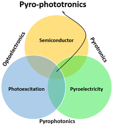 | ||
| Fig. 15 Schematic diagram of the pyro-phototronic effect.114 | ||
There are four stages involved in the pyro-phototronic effect that occur during one period of light being turned ON and OFF.115,120,121 These stages are also reflected in the transient response of the self-powered device, as demonstrated in Fig. 16.
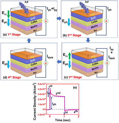 | ||
| Fig. 16 (a–d) Four stages of pyro-phototronic effect, and (e) time response, of an ITO/ZnO QD/CdSe QD/MoOx/Au-based self-powered photodetector.115 | ||
• 1ststage: the initial stage of the pyro-phototronic effect involves the incidence of light on the semiconductor surface, which generates a temperature gradient. The duration of this gradient is brief, but it results in a net electric displacement due to the redistribution of charges on the surface. As a result, a temporary electric potential, known as pyro-potential, develops across the device, which is additive to the built-in potential. This leads to an increase in the resulting potential difference across the device, causing the movement of photogenerated charge carriers more efficiently toward the electrodes. The total current consists of two components: the photocurrent (Iph) due to the built-in electric potential and the pyro-current (Ipy) due to the pyro-potential. This stage is indicated as the 1st stage in Fig. 16(a) and (e).
• 2ndstage: after a short period, the temperature gradient will start to decrease, causing a reduction in the pyro-current as indicated by eqn (18). As a result, the net effect on the device photocurrent will be an exponential decay due to the reduction in Ipy, and the net current will eventually saturate to a value equal to the photocurrent (Iph). This stage is illustrated in Fig. 16(b) and (e) as the second stage.
• 3rdstage: when the light is turned OFF abruptly, it results in a negative temperature gradient, which leads to the development of pyro-potential in the opposite direction to the built-in potential. This pyro-potential supports the recombination mechanism, reducing the carrier lifetime and causing a sudden decrease in current. This stage is illustrated as the third stage in Fig. 16(c) and (e).
• 4thstage: once the negative temperature gradient diminishes, the device returns to its thermal equilibrium state, as shown in the fourth stage of Fig. 16(d) and (e).
The pyro-phototronic effect leads to improved figures of merit such as detectivity, response time, responsivity, and EQE.116 Chen et al.86 demonstrated a self-powered photodetector based on AZO/ZnO/graphene, which utilized the pyro-phototronic effect. The device shows a good transient response with a 32 ms rise/fall time and a reported responsivity of 50 μA W−1. The pyro-phototronic effect was also employed by Boruah et al.64 along with a carrier transport layer of PEDOT:PSS and an active layer of ZnO NRs to achieve an improved transient response. The fabricated device demonstrated a rise time of 28 ms and a fall time of 23 ms,64 with an enhanced responsivity of 2.2254 mA W−1. To enhance the temperature gradient across the pyroelectric thin film, researchers have explored the use of energy exchange from indirect bandgap semiconductors. Chen et al.122 utilized a Si-substrate (indirect bandgap semiconductor) and ZnO NWs (pyroelectric material) to achieve this. They reported an improved transient response with a rise time of 15 μs and a fall time of 21 μs due to the enhanced pyro-phototronic effect. Rana et al.121 demonstrated that the figures of merit of self-powered devices could be further improved by utilizing a 100% illumination area. They fabricated an FTO/ZnO/NiO/Ag NW-based device, which exhibited a rise and fall time of 3.92 μs each and an improved responsivity of 290 mA W−1. Similarly, Silva et al.120 utilized a 100% illumination area and fabricated an ITO/ZnO/SnOx/Si/Al-based self-powered device with an excellent transient response as shown in Fig. 17. The device exhibited a rise time of 2 μs, a fall time of 3 μs, and a responsivity of 64.1 mA W−1.
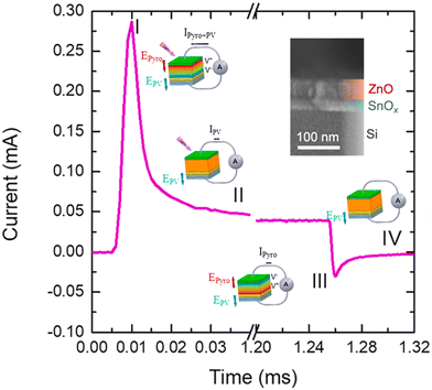 | ||
| Fig. 17 Time response of an ITO/ZnO/SnOx/Si/Al-based self-powered device with insets indicating four stages and a schematic.120 Copyright “Elsevier”, 2021 (included with permission). | ||
The effect of a nanostructured semiconductor is also studied to improve the pyro-phototronic effect. Nanostructures exhibit higher polarization than their bulk counterparts, as reported by Zhang et al.124 For instance, GaN NWs show pyroelectric coefficients that are 4.6 times higher than bulk GaN; this is attributed to the small-scale effect.125 Therefore, quantum dots are most suitable for tunable self-powered photodetectors that utilize the pyroelectric effect. Goel and Kumar115 employed ZnO QDs and CdSe QDs in combination with MoOx as the hole transport layer to fabricate their device. The resulting device exhibited a sensitivity of approximately 330, a FWHM of 57 nm, and an EQE of 3.79%. Recently, Qiao et al.123 reported an ITO ZnO NW/Si-based device to depict the dependence of the pyro-phototronic effect on the NWs’ length. In the same article, they reported an ITO/ZnO NWs/PEDOT:PSS/Ag-based device as shown in Fig. 18(a). The transient characteristics shown in Fig. 18(b) indicate the increase in the pyro-phototronic effect with decreasing NW length. The pyro-phototronic effect depends on many factors associated with the device, such as junction type, transport layer, and electrode.
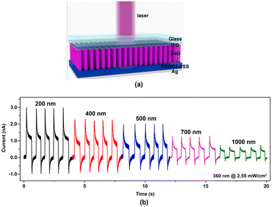 | ||
| Fig. 18 (a) Schematic of an ITO/ZnO NW/PEDOT:PSS/Ag-based device. (b) Time response for different nanowire lengths.123 Copyright “Elsevier”, 2022 (included with permission). | ||
• Effect of a heterojunction: Kumar et al.92 developed a device based on an ITO/ZnO QDs/CdSe QDs/Au heterojunction, as depicted in Fig. 19(a). This device employs a heterojunction between CdSe and ZnO. Its transient response exhibits pyroelectric behavior with a pyroelectric current of 0.1 μA cm−2, as demonstrated in Fig. 19(b). In addition, Kumar et al.82 also fabricated a hybrid heterojunction device consisting of ITO/PQT-12/CdSe QDs/Au, as shown in Fig. 19(a). In contrast to ZnO QDs, PQT-12 is an organic polymer with pyroelectric properties. The pyroelectric current density in both devices is almost identical, as indicated in Fig. 19(b) and (c), although the PQT-12-based device has a lower overall current (i.e., the sum of photocurrent and pyrocurrent) compared to the ZnO QD-based device due to the low mobility of organic materials. This PQT-12-based device has broad-spectrum coverage. Conversely, the ZnO QD-based device has narrowband detection capabilities, making it suitable for colour detection and image sensing applications.4,12
 | ||
| Fig. 19 (a) ITO/(ZnO QD, PQT-12)/CdSe QD/Au-based device, (b) transient response of ZnO QD-based device, and (c) transient response of PQT-12-based device under white light illumination.82,92 | ||
• Effect of the transport layer: as discussed earlier, the HTL plays a significant role in optoelectronic devices. In addition, the HTL can also impact the pyroelectric current in the device. Goel et al.115 highlighted the advantages of incorporating the MoOx layer as an HTL. They fabricated a device consisting of ITO/ZnO QDs/CdSe QDs/MoOx/Au and compared its performance with the reported device that did not use MoOx![[thin space (1/6-em)]](https://www.rsc.org/images/entities/char_2009.gif) 92 while keeping all other layers the same. The results showed that the utilization of the MoOx layer increased the pyroelectric current density from 0.1 μA cm−2 to 1.75 μA cm−2. Hence, HTLs can also be employed to modify the pyroelectric response of the device.
92 while keeping all other layers the same. The results showed that the utilization of the MoOx layer increased the pyroelectric current density from 0.1 μA cm−2 to 1.75 μA cm−2. Hence, HTLs can also be employed to modify the pyroelectric response of the device.
• Impact of electrodes: a device's electrical and optical properties are significantly influenced by metal electrodes.126 Kumar et al.92 conducted a study to compare the performance of self-powered photodetectors comprising ITO/ZnO QDs/CdSe QDs/electrodes by changing the electrode material. They used Au and Pd as the electrodes and found that the device's performance could be enhanced by selecting the appropriate electrode. From the transient response of the devices, it was observed that the pyroelectric behavior was noticeable only in Au-based devices, with a pyroelectric current of 0.1 μA cm−2, even though the device structures were similar. Goel and Kumar53 fabricated an ITO/ZnO QDs/CdSe QDs/MoOx/Pd-based device, as shown in Fig. 20(a), which showed little pyroelectric behaviour, with a pyroelectric current density of 0.587 μA cm−2, as shown in Fig. 20(b). They also reported a device based on ITO/ZnO QDs/CdSe QDs/MoOx/Au, similar to the previous structure, but with a change in the electrode material, as shown in Fig. 20(a). This device showed a pyroelectric current density of 1.75 μA cm−2, as shown in Fig. 20(c). Therefore, it can be concluded that the pyroelectric behaviour is dominant in Au electrode-based devices compared to Pd electrode-based devices.
 | ||
| Fig. 20 (a) ITO/ZnO QD/CdSe QD/MoOx/(Pd,Au)-based device, (b) transient response of Pd-based device and (c) transient response of Au-based device under white light illumination.92 | ||
A list of different devices utilizing the pyro-phototronic effect is given in Table 6.
| Structure | I ph (nA) | I py (nA) | Rise time (ms) | Fall time (ms) | Detectivity (Jones) | Responsivity (mA W−1) | EQE (%) | FWHM (nm) |
|---|---|---|---|---|---|---|---|---|
| FTO/ZnO/MAPbI3/spiro-OMeTAD/Cu127 | 1500 | 1250 | 0.053 | 0.063 | 4.50 × 10¹⁰ | — | — | — |
| ITO/ZnO NW/p-Si/Cu128 | 350 | 800 | 1.2 | 1.3 | 1.40 × 10⁹ | 13 | — | — |
| FTO/ZnO NW/MAPbI3/spiro-OMeTAD/Cu129 | 200 | 300 | 0.01 | — | — | — | — | — |
| Al-ZnO NR/NiO/Si130 | 100 | 200 | — | — | — | — | — | — |
| ITO/Cl:ZnO NW/PEDOT PSS/Ag64 | 220 | 344 | 28 | 23 | 1.54 × 10¹⁰ | 2.2254 | 0.792 | <100 |
| PET/ITO/ZnO/Ag131 | 5 | 70 | 4.5 | 3.5 | 2.70 × 10⁹ | 1.25 | — | — |
| FTO/ZnO/p-NiO/Ag NW121 | 100![[thin space (1/6-em)]](https://www.rsc.org/images/entities/char_2009.gif) 000 000 |
400![[thin space (1/6-em)]](https://www.rsc.org/images/entities/char_2009.gif) 000 000 |
0.00392 | 0.0089 | 2.75 × 10¹¹ | 290 | — | — |
| ITO/ZnO/ZnTe/Al132 | 500 | 3500 | 0.062 | 0.109 | 3.47 × 10¹² | 196.24 | — | >100 |
| AZO/ZnO/graphene86 | 200 | 2200 | 32 | 32 | — | 0.05 | — | — |
| ITO/ZnO/p-Si/Ag133 | 1100 | 400 | 0.6 | 0.5 | 24.6 × 10⁹ | 79.9 | — | — |
| ITO/ZnO NW/p-Si/Cu119 | 780 | 4670 | 0.015 | 0.021 | 8.78 × 10¹¹ | 164 | — | >100 |
| n-Si/ZnO NW/PEDOT:PSS134 | 100 | 1400 | — | — | — | 22.054 | — | — |
| ITO/ZnO/SnOx/Si/Al17 | 50![[thin space (1/6-em)]](https://www.rsc.org/images/entities/char_2009.gif) 000 000 |
250![[thin space (1/6-em)]](https://www.rsc.org/images/entities/char_2009.gif) 000 000 |
0.002 | 0.003 | 2.40 × 10¹¹ | 64.1 | — | >100 |
| Cr/Au/BTO/p-GaN/Au/Cr135 | 560![[thin space (1/6-em)]](https://www.rsc.org/images/entities/char_2009.gif) 000 000 |
670![[thin space (1/6-em)]](https://www.rsc.org/images/entities/char_2009.gif) 000 000 |
160 | 235 | — | — | — | — |
| ITO/ZnO/Si123 | 1.5 | 2 | — | — | 2.44 × 10¹¹ | 0.565 | — | — |
| ITO/ZnO QDs/CdSe QDs/MoOx/Au115 | 187.5 | 131.25 | 9.69 | 15.66 | 1.77 × 10¹⁰ | 12.2 | 3.79 | 57 |
| FTO/CQDs-ZNO NR/PEDOS/FTO136 | 30 | 30 | 78 | 77 | 5.00 × 10¹⁰ | 10 | — | — |
9.2 Piezo-phototronic effect
Pyroelectric and piezoelectric behavior can be observed in 10 out of 32 crystal structures, particularly those with a wurtzite structure such as ZnO, CdSe, InN, and GaN. These materials exhibit anisotropic behaviour in various directions, resulting in piezoelectricity. In self-powered photodetectors, mechanical stress and strain can be utilized to modulate charge carrier generation, separation, extraction, and recombination phenomena. The piezoelectric effect in materials generates an electrical potential when subjected to mechanical stress. When combined with the photovoltaic effect caused by incident photons, this phenomenon is referred to as the piezo-phototronic effect. A schematic of the piezo-phototronic effect is shown in Fig. 21, indicating that the piezo-phototronic effect as the combination of a semiconductor, photoexcitation, and piezoelectricity. This effect is particularly useful for flexible, wearable self-powered devices, as it has been shown to improve performance by up to 70%.139 Two-dimensional atomically thin materials and one-dimensional wurtzite NWs are ideal for flexible device fabrication as they can withstand significant strain.79 Zhang et al.138 fabricated a ZnO NRA-based self-powered photodetector that incorporated the piezo-phototronic effect, as illustrated in Fig. 22. When subjected to compressive strain, the detector's responsivity increased by approximately 2.75 times compared to when no strain was applied. Zhang et al.140 reported a flexible MoS2 p–n junction-based photodiode. This device offered a performance improvement by 319% due to the piezo-phototronic effect. MoS2 can be used along with ZnO and CuO for the preparation of a self-powered photodetector utilizing the piezo-phototronic effect.141,142 Other effects like flexophototronic143 and photogating144 can also be used in conjunction with the piezo-phototronic effect in self-powered photodetectors.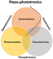 | ||
| Fig. 21 Schematic of the piezo-phototronic effect.137 | ||
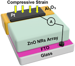 | ||
| Fig. 22 Schematic of a self-powered photodetector utilizing the piezo-phototronic effect.138 | ||
9.3 Plasmonics
Metal nanoparticles can guide and confine light within a semiconductor by generating plasmons, which are oscillations of free electrons on the surface of the metal. These plasmons can interact with incoming light, enhancing the electric field near the surface of the solar cell/photodetector. The use of plasmonics has been shown to enhance the efficiency of photovoltaic devices significantly,145,146 and it has also been applied to self-powered photodetectors. Plasmonics can be utilized in three ways:1. Front surface scattering: plasmonic nanoparticles can be used on the device's front surface as shown in Fig. 23(a). This approach traps light by scattering the light within the semiconductor layer (absorber layer) when the wavelength of light is greater than the size of the metal nanoparticle. A point model described this phenomenon of light absorption and scattering. The scattering and absorption cross sections can be written as:147
 | (20) |
 | (21) |
 | ||
| Fig. 23 Illustration of (a) front surface scattering, (b) sub-wavelength antenna, and (c) back surface corrugation.146 Copyright “Nature Publishing Group”, 2010 (included with permission). | ||
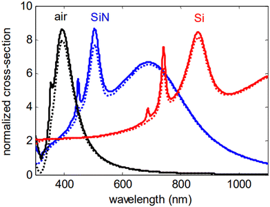 | ||
| Fig. 24 Variation of scattering (dashed) and absorption cross-section (solid) of Ag-plasmonic nanoparticle embedded in different media.147 Published with “Optica Publishing Group” as open access, 2008. | ||
2. Sub-wavelength antenna: metallic nanoparticles are used as sub-wavelength antennas where the plasmonic near field and semiconductor are coupled and hence increase the effective absorption cross-section width as shown in Fig. 23(b). The efficiency of solar energy harvesting through nanoantennas heavily relies on their radiation efficiency.149 The radiation efficiency is directly influenced by the type of metal used as a conductor and the size of the nanoantenna. The total radiation efficiency can be written as:150
 | (22) |
 | (23) |
3. Back surface corrugation: corrugations are small, regularly spaced indentations or bumps added to the solar cell/photodetector's surface. These indentations scatter incoming light, causing it to travel a longer distance through the device and increasing the probability that it will be absorbed. A corrugated metal film is used at the back surface. This efficiently couples sunlight in the surface plasmon polariton at the metal–semiconductor junction and increases the effective absorption thickness146 as shown in Fig. 23(c).
Light trapping is particularly noticeable at the peak of the plasmon resonance spectrum (the reflectance versus frequency plot obtained using surface plasmon resonance excitation). This effect can be further adjusted using a dielectric in the surrounding medium. For instance, when small gold or silver nanoparticles are in the air, their plasmon resonance occurs at 480 nm and 350 nm, respectively. However, by employing commonly used materials like SiO2, Si3N4, or Si in the manufacturing of solar cells, it is possible to shift these plasmon resonances across a range of 500 nm to 1500 nm.146 Plasmonics help to efficiently reduce the thickness of the active layer. By reducing the thickness, both its cost-effectiveness and electrical properties can be improved. This is because a decrease in thickness reduces the dark current and increases the open-circuit voltage. Additionally, carrier recombination is minimized when carriers only travel a short distance before being collected at the junction, resulting in a higher photocurrent. Yu et al.153 fabricated a self-powered photodetector using βGa2O3/NiO and designed it for solar-blind applications. The authors investigated the potential of inducing a plasmonic effect with Pt nanoparticles. They found that by utilizing the Pt nanoparticles, the responsivity, EQE, and rise/decay time increased from 0.245 to 4.27 mA W−1, 0.72 to 1.97%, and 12/8 to 4.6/7.6 ms, respectively. Dai et al.151 fabricated a dual-band self-powered photodetector using surface plasmon polarization as shown in Fig. 25. In this device, Au nanoparticles have been patterned on the InSe nanosheets as shown in Fig. 25(b). This device can sense photons from the visible to NIR regions. At 0 V, this device has 369 and 244 mA W−1 responsivities at 365 and 685 nm wavelengths. Hussain et al.152 fabricated a plasma polymerized aniline-TiN (PPATiN) based broadband photodetector as shown in Fig. 26. This device shows enhanced figures of merit at low-intensity irradiance of 3.5 mW cm−2. The responsivity of the device is 570 mA W−1 at zero bias. Lu et al. fabricated an Ag NP-based graphene/GaAs heterojunction. They just spun the layer of Ag nanoparticles onto the graphene/GaAs surface and found exceptional results. The responsivity is increased by 38% while the detectivity is increased by 202%. This broadband device operates from 325 to 900 nm, peaking at ∼405 nm.
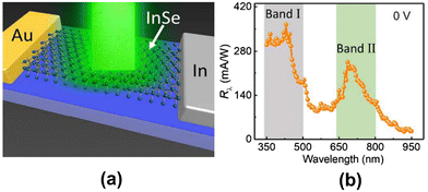 | ||
| Fig. 25 (a) Schematic, and (b) responsivity versus wavelength of the plasmon-based InSe/Au dual-band self-powered photodetector.151 Copyright “American Chemical Society”, 2018 (included with permission). | ||
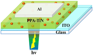 | ||
| Fig. 26 Schematic of PPA-TiN-based hybrid photodetector.152 Copyright “American Chemical Society”, 2016 (included with permission). | ||
Recently, Silva et al.154 reported the tri-layered heterojunction of n-Si/p-SnO/n-ZnO as shown in Fig. 27(a). They incorporated a plasmonic effect utilizing Ag nanoparticles. The three synergistic effects, namely, photovoltaic, pyro-phototronic, and plasmonic, resulted in a responsivity of 210.2 mA W−1 and a rise (fall) time of 2.3 (51.3) μs. The energy band diagram in Fig. 27(b) indicates the development of a dual built-in electric field. However, the electric field developed due to the light-induced pyro-phototronic effect results in efficient carrier collection.
 | ||
| Fig. 27 (a) Schematic representation of synergistic effects, namely, photovoltaic, pyro-phototronic, and plasmonic in the Al/Si/SnO/Ag NP/ZnO/ITO device, and (b) energy band diagram.154 Published with “Royal Society of Chemistry” as open access, 2024. | ||
The utilization of polarization-sensitive materials results in improved figures of merit. Zhao et al. prepared a self-powered photodetector utilizing MoSe2 and Te with a van der Waals heterojunction with a strong interlayer transition.155 This device offered an extremely high detectivity in the order of ∼1013 Jones and could be utilized to detect weak signals efficiently.
10 Perspective and summary
This review highlights the importance of adopting a suitable device engineering approach to improve the performance of self-powered photodetectors. It has been observed that the response time of a self-powered photodetector is higher than that of a conventional photodetector, which opens an area for researchers to investigate.Material innovations may meet future requirements. The utilization of the perovskite QDs and 2D materials like MoS2, MoSe2, MXenes etc. could be the materials of choice. For example, flexible electronics will require a substrate with good mechanical strength, which can be achieved using 2D materials. The device with an organic material as an active layer requires a superior ETL and HTL. Spectrum selectivity can be improved by utilizing a good pyroelectric semiconducting material along with other novel functional materials with tunable band gap behaviour (colloidal QDs and 2D MXenes).
Several techniques can be utilized to enhance the performance of self-powered photodetectors, including ETL, HTL, bandgap and junction engineering and exploiting the piezo-phototronic and pyro-phototronic effects and plasmonics. These techniques hold significant potential for revolutionizing self-powered photodetectors, which are expected to play a vital role in future IoT networks and communication systems. Therefore, further research on these techniques could lead to significant advancements in the field of self-powered photodetectors. Moreover, mimicking the human eye's functioning is an exciting prospect for self-powered photodetectors. Researchers are exploring the possibility of developing self-powered photodetectors that mimic the human eye's structure and functioning, such as its high sensitivity and dynamic range. This could lead to the development of artificial vision systems that can detect, process, and respond to visual information without requiring external power sources. In addition, recent advancements in materials science and nanotechnology have enabled the development of novel materials and devices that can improve the efficiency and performance of self-powered photodetectors. For example, using 2D materials, such as graphene and transition metal dichalcogenides, has shown promising results in enhancing the photoresponsivity of self-powered photodetectors. Overall, the future of self-powered photodetectors looks promising. With further research and development, these devices can play a vital role in powering next-generation IoT networks, communication systems, and artificial vision systems.
Author contributions
Varun Goel: conceptualization, data curation, investigation, methodology, visualization, writing – original draft. Yogesh Kumar: formal analysis, funding acquisition, methodology, resources, validation, writing – review & editing. Gopal Rawat: funding acquisition, methodology, supervision, validation, writing – review & editing. Hemant Kumar: conceptualization, formal analysis, funding acquisition, investigation, methodology, resources, supervision, writing – review & editing.Conflicts of interest
There are no conflicts to declare.Acknowledgements
This work was supported in part by the Science and Engineering Research Board (SERB) through the Department of Science and Technology (DST), Government of India, under grant nos. SRG/2020/001282, EEQ/2022/000141, EEQ/2020/000183 and SRG/2020/000461.References
- J. J. Cadusch, J. Meng, B. J. Craig, V. R. Shrestha and K. B. Crozier, Nanophotonics, 2020, 9, 3197–3208 CrossRef CAS.
- R. A. Dias, J. H. Correia and G. Minas, 2007 IEEE International Symposium on Industrial Electronics, 2007, pp. 2747–2751.
- W. W. Moses, Nucl. Instrum. Methods Phys. Res., Sect. A, 2009, 610, 11–15 CrossRef CAS PubMed.
- R. D. Jansen-van Vuuren, A. Armin, A. K. Pandey, P. L. Burn and P. Meredith, Adv. Mater., 2016, 28, 4766–4802 CrossRef CAS PubMed.
- F. Rutz, A. Bächle, R. Aidam, J. Niemasz, W. Bronner, A. Zibold and R. Rehm, Infrared Technology and Applications XLV, 2019, p. 1100211 Search PubMed.
- N. Martini, V. Koukou, G. Fountos, I. Valais, A. Bakas, K. Ninos, I. Kandarakis, G. Panayiotakis and C. Michail, Procedia Struct. Integr., 2018, 10, 326–332 CrossRef.
- S. Liu, X. Zhang, X. Gu and D. Ming, Biosens. Bioelectron., 2019, 143, 111617 CrossRef CAS PubMed.
- C. Choi, M. K. Choi, S. Liu, M. Kim, O. K. Park, C. Im, J. Kim, X. Qin, G. J. Lee, K. W. Cho, M. Kim, E. Joh, J. Lee, D. Son, S.-H. Kwon, N. L. Jeon, Y. M. Song, N. Lu and D.-H. Kim, Nat. Commun., 2017, 8, 1–11 CrossRef PubMed.
- C. I. Rablau , Fifteenth Conference on Education and Training in Optics and Photonics: ETOP 2019, 2019, pp. 1–14.
- T. Mueller, F. Xia and P. Avouris, Nat. Photonics, 2010, 4, 297–301 CrossRef CAS.
- M. Masoud, Y. Jaradat, A. Manasrah and I. Jannoud, J. Sens., 2019, 2019, 1–26 CrossRef.
- Q. Lin, A. Armin, P. L. Burn and P. Meredith, Nat. Photonics, 2015, 9, 687–694 CrossRef CAS.
- M. Peng, Y. Liu, A. Yu, Y. Zhang, C. Liu, J. Liu, W. Wu, K. Zhang, X. Shi, J. Kou, J. Zhai and Z. L. Wang, ACS Nano, 2015, 10, 1572–1579 CrossRef PubMed.
- A. Bera, A. D. Mahapatra, S. Mondal and D. Basak, ACS Appl. Mater. Interfaces, 2016, 8, 34506–34512 CrossRef CAS PubMed.
- G. Rawat, D. Somvanshi, Y. Kumar, H. Kumar, C. Kumar and S. Jit, IEEE Trans. Nanotechnol., 2016, 1–1 Search PubMed.
- H. Lu, W. Tian, F. Cao, Y. Ma, B. Gu and L. Li, Adv. Funct. Mater., 2016, 26, 1296–1302 CrossRef CAS.
- W. Tian, Y. Wang, L. Chen and L. Li, Small, 2017, 13, 1701848 CrossRef PubMed.
- W. Ouyang, J. Chen, Z. Shi and X. Fang, Appl. Phys. Rev., 2021, 8, 031315 CAS.
- A. R. Jayakrishnan, J. P. Silva, K. Gwozdz, M. J. Gomes, R. L. Hoye and J. L. MacManus-Driscoll, Nano Energy, 2023, 118, 108969 CrossRef CAS.
- M. F. Al Fattah, A. A. Khan, H. Anabestani, M. M. Rana, S. Rassel, J. Therrien and D. Ban, Nanoscale, 2021, 13, 15526–15551 RSC.
- C. Perumal Veeramalai, S. Feng, X. Zhang, S. V. N. Pammi, V. Pecunia and C. Li, Photonics Res., 2021, 9, 968 CrossRef.
- R. Hui, Introduction to Fiber-Optic Communications, Elsevier, 2020, pp. 125–154 Search PubMed.
- B. N. Pal, I. Robel, A. Mohite, R. Laocharoensuk, D. J. Werder and V. I. Klimov, Adv. Funct. Mater., 2012, 22, 1741–1748 CrossRef CAS.
- J. Liu, M. Gao, J. Kim, Z. Zhou, D. S. Chung, H. Yin and L. Ye, Mater. Today, 2021, 51, 475–503 CrossRef CAS.
- C.-T. Lee, T.-S. Lin and H.-Y. Lee, IEEE Photonics Technol. Lett., 2010, 22, 1117–1119 CAS.
- M. Z. Nawaz, L. Xu, X. Zhou, K. H. Shah, J. Wang, B. Wu and C. Wang, Mater. Adv., 2021, 2, 6031–6038 RSC.
- X. Zhang, M. Dai, W. Deng, Y. Zhang and Q. J. Wang, Nanophotonics, 2023, 12, 607–618 CrossRef CAS.
- T. Kirchartz, J. Bisquert, I. Mora-Sero and G. Garcia-Belmonte, Phys. Chem. Chem. Phys., 2015, 17, 4007–4014 RSC.
- M. Ding, Z. Guo, X. Chen, X. Ma and L. Zhou, Nanomaterials, 2020, 10, 362 CrossRef CAS PubMed.
- P. Zheng, J. Yang, Z. Wang, L. Wu, H. Sun, S. Chen, Y. Guo, H. Xia, S. P. Phang, E.-C. Wang, J. Stuckelberger, H. C. Sio, X. Zhang, D. Macdonald and H. Jin, Cell Rep. Phys. Sci., 2021, 2, 100603 CrossRef CAS.
- R. Sharma, Heliyon, 2019, 5, e01965 CrossRef CAS PubMed.
- D. Yang, L. Zhang, H. Wang, Y. Wang, Z. Li, T. Song, C. Fu, S. Yang and B. Zou, IEEE Photonics Technol. Lett., 2015, 27, 233–236 CAS.
- M. D. Ward, W. Shi, N. Gasparini, J. Nelson, J. Wade and M. J. Fuchter, J. Mater. Chem. C, 2022, 10, 10452–10463 RSC.
- A. P. Singh, R. K. Upadhyay and S. Jit, IEEE Trans. Electron Devices, 2022, 69, 3230–3235 CAS.
- B. G. Streetman and S. Banerjee, Solid State Electronic Devices, Pearson, 7th edn, 2017 Search PubMed.
- D. K. Jarwal, C. Dubey, K. Baral, A. Bera and G. Rawat, IEEE Trans. Electron Devices, 2022, 69, 5012–5020 CAS.
- P. K. Mishra, S. Ayaz, T. Srivastava, S. Tiwari, R. Meena, B. Kissinquinker, S. Biring and S. Sen, J. Mater. Sci.: Mater. Electron., 2019, 30, 18686–18695 CrossRef CAS.
- D. Somvanshi, D. Chauhan, A. G. U. Perera, L. Li, L. Chen and E. H. Linfield, IEEE Sens. Lett., 2019, 3, 1–4 Search PubMed.
- V. Goel and H. Kumar, IEEE Photonics Technol. Lett., 2023, 35, 911–914 CAS.
- N. Yamada, Y. Kondo, X. Cao and Y. Nakano, Appl. Mater. Today, 2019, 15, 153–162 CrossRef.
- A. V. Babichev, H. Zhang, P. Lavenus, F. H. Julien, A. Y. Egorov, Y. T. Lin, L. W. Tu and M. Tchernycheva, Appl. Phys. Lett., 2013, 103, 201103 CrossRef.
- D. Bera, L. Qian, T.-K. Tseng and P. H. Holloway, Materials, 2010, 3, 2260–2345 CrossRef CAS.
- C. Giansante, Chem. – Eur. J., 2021, 27, 14358–14368 CrossRef PubMed.
- A. P. Alivisatos, Science, 1996, 271, 933–937 CrossRef CAS.
- Y.-Q. Bie, Z.-M. Liao, H.-Z. Zhang, G.-R. Li, Y. Ye, Y.-B. Zhou, J. Xu, Z.-X. Qin, L. Dai and D.-P. Yu, Adv. Mater., 2010, 23, 649–653 CrossRef PubMed.
- X. X. Liu and J. R. Sites, J. Appl. Phys., 1994, 75, 577–581 CrossRef CAS.
- S. Xu, Y. Qin, C. Xu, Y. Wei, R. Yang and Z. L. Wang, Nat. Nanotechnol., 2010, 5, 366–373 CrossRef CAS PubMed.
- W. Wu, S. Bai, M. Yuan, Y. Qin, Z. L. Wang and T. Jing, ACS Nano, 2012, 6, 6231–6235 CrossRef CAS PubMed.
- J. Xu and G. Shen, Nano Energy, 2015, 13, 131–139 CrossRef CAS.
- D. A. Neamen, Semiconductor physics and devices: basic principles, McGraw-Hill, New York, NY, 4th edn, 2012 Search PubMed.
- Y. Xie, L. Wei, Q. Li, G. Wei, D. Wang, Y. Chen, J. Jiao, S. Yan, G. Liu and L. Mei, Appl. Phys. Lett., 2013, 103, 261109 CrossRef.
- H. Kumar, Y. Kumar, B. Mukherjee, G. Rawat, C. Kumar, B. N. Pal and S. Jit, IEEE J. Quantum Electron., 2017, 53, 1–8 Search PubMed.
- V. Goel and H. Kumar, IEEE Photonics Technol. Lett., 2022, 34, 1273–1276 CAS.
- K. Shen, H. Xu, X. Li, J. Guo, S. Sathasivam, M. Wang, A. Ren, K. L. Choy, I. P. Parkin, Z. Guo and J. Wu, Adv. Mater., 2020, 32, 2000004 CrossRef CAS PubMed.
- H. Zhou, L. Yang, P. Gui, C. R. Grice, Z. Song, H. Wang and G. Fang, Sol. Energy Mater. Sol. Cells, 2019, 193, 246–252 CrossRef CAS.
- Y. Li, H. Chen and J. Zhang, Nanomaterials, 2021, 11, 1404 CrossRef CAS PubMed.
- E. Voroshazi, I. Cardinaletti, G. Uytterhoeven, A. Hadipour, B. P. Rand and T. Aernouts, 2013 IEEE 39th Photovoltaic Specialists Conference (PVSC), 2013, pp. 3212–3215.
- T. Edvinsson, R. Soc. Open Sci., 2018, 5, 180387 CrossRef CAS PubMed.
- H. Kumar, Y. Kumar, G. Rawat, C. Kumar, B. Mukherjee, B. N. Pal and S. Jit, IEEE Trans. Nanotechnol., 2017, 16, 1073–1080 CAS.
- L. Hu and A. Mandelis, J. Appl. Phys., 2021, 129, 091101 CrossRef CAS.
- C. B. Murray, D. J. Norris and M. G. Bawendi, J. Am. Chem. Soc., 1993, 115, 8706–8715 CrossRef CAS.
- C. J. Murphy, Anal. Chem., 2002, 74, 520 A–526 A CrossRef CAS PubMed.
- R. H. Gilmore, E. M. Y. Lee, M. C. Weidman, A. P. Willard and W. A. Tisdale, Nano Lett., 2017, 17, 893–901 CrossRef CAS PubMed.
- B. D. Boruah, S. N. Majji, S. Nandi and A. Misra, Nanoscale, 2018, 10, 3451–3459 RSC.
- F. Abbasi, F. Zahedi and M. hasan Yousefi, J. Mater. Sci.: Mater. Electron., 2021, 32, 19614–19625 CrossRef CAS.
- K. D. A. Kumar, P. Mele, S. Golovynskyi, A. Khan, A. M. El-Toni, A. A. Ansari, R. K. Gupta, H. Ghaithan, S. AlFaify and P. Murahari, J. Alloys Compd., 2022, 892, 160801 CrossRef CAS.
- D. Alonso-Álvarez, T. Wilson, P. Pearce, M. Führer, D. Farrell and N. Ekins-Daukes, J. Comput. Electron., 2018, 17, 1099–1123 CrossRef.
- D. P. Joseph and C. Venkateswaran, J. At., Mol., Opt. Phys., 2011, 2011, 1–7 CrossRef.
- C.-Z. Ning, L. Dou and P. Yang, Nat. Rev. Mater., 2017, 2, 17070 CrossRef CAS.
- D. Singh, N. Singh, S. D. Sharma, C. Kant, C. P. Sharma, R. R. Pandey and K. K. Saini, J. Sol-Gel Sci. Technol., 2010, 58, 269–276 CrossRef.
- Q. Hao, H. Yi, J. Liu, Y. Wang, J. Chen, X. Yin, C. S. Tang, D. Qi, H. Gan, A. T. S. Wee, Y. Chai and W. Zhang, Adv. Opt. Mater., 2022, 10, 2200063 CrossRef CAS.
- M. Yu, F. Gao, Y. Hu, L. Wang, P. Hu and W. Feng, J. Colloid Interface Sci., 2020, 565, 239–244 CrossRef CAS PubMed.
- S. Ebrahimi and B. Yarmand, J. Alloys Compd., 2020, 827, 154246 CrossRef CAS.
- E. Delli, V. Letka, P. D. Hodgson, E. Repiso, J. P. Hayton, A. P. Craig, Q. Lu, R. Beanland, A. Krier, A. R. J. Marshall and P. J. Carrington, ACS Photonics, 2019, 6, 538–544 CrossRef CAS.
- F. Capasso, Physica B+C, 1985, 129, 92–106 CrossRef CAS.
- F. Li, Y. Meng, R. Dong, S. Yip, C. Lan, X. Kang, F. Wang, K. S. Chan and J. C. Ho, ACS Nano, 2019, 13, 12042–12051 CrossRef CAS PubMed.
- V. Goel and H. Kumar, in Self-Powered Photodetectors: Fundamentals and Recent Advancements, Bentham Science Publishers, 2023, pp. 256–291 Search PubMed.
- H. Shen, C. X. Shan, B. H. Li, B. Xuan and D. Z. Shen, Appl. Phys. Lett., 2013, 103, 232112 CrossRef.
- X. Hu, X. Li, G. Li, T. Ji, F. Ai, J. Wu, E. Ha and J. Hu, Adv. Funct. Mater., 2021, 31, 2011284 CrossRef CAS.
- J. J. Hassan, M. A. Mahdi, S. J. Kasim, N. M. Ahmed, H. A. Hassan and Z. Hassan, Appl. Phys. Lett., 2012, 101, 261108 CrossRef.
- V. Goel and H. Kumar, 2023 International Conference on Recent Advances in Electrical, Electronics & Digital Healthcare Technologies (REEDCON), 2023, pp. 47–49.
- H. Kumar, Y. Kumar, G. Rawat, C. Kumar, B. Mukherjee, B. N. Pal and S. Jit, IEEE Photonics Technol. Lett., 2017, 29, 1715–1718 Search PubMed.
- K. Li, Y. Lu, X. Yang, L. Fu, J. He, X. Lin, J. Zheng, S. Lu, C. Chen and J. Tang, InfoMat, 2021, 3, 1145–1153 CrossRef CAS.
- B. D. Boruah, A. Mukherjee and A. Misra, Nanotechnology, 2016, 27, 095205 CrossRef PubMed.
- L. Duan, F. He, Y. Tian, B. Sun, J. Fan, X. Yu, L. Ni, Y. Zhang, Y. Chen and W. Zhang, ACS Appl. Mater. Interfaces, 2017, 9, 8161–8168 CrossRef CAS PubMed.
- D. Chen, Y. Xin, B. Lu, X. Pan, J. Huang, H. He and Z. Ye, Appl. Surf. Sci., 2020, 529, 147087 CrossRef CAS.
- H.-Y. Chen, K.-W. Liu, X. Chen, Z.-Z. Zhang, M.-M. Fan, M.-M. Jiang, X.-H. Xie, H.-F. Zhao and D.-Z. Shen, J. Mater. Chem. C, 2014, 2, 9689–9694 RSC.
- M. Mishra, A. Gundimeda, T. Garg, A. Dash, S. Das, Vandana and G. Gupta, Appl. Surf. Sci., 2019, 478, 1081–1089 CrossRef CAS.
- K. Benyahia, F. Djeffal, H. Ferhati, A. Bendjerad, A. Benhaya and A. Saidi, J. Alloys Compd., 2021, 859, 158242 CrossRef CAS.
- Y. Purusothaman, N. R. Alluri, A. Chandrasekhar, V. Vivekananthan and S.-J. Kim, J. Phys. Chem. C, 2018, 122, 12177–12184 CrossRef CAS.
- Y. Chang, L. Chen, J. Wang, W. Tian, W. Zhai and B. Wei, J. Phys. Chem. C, 2019, 123, 21244–21251 CrossRef CAS.
- H. Kumar, Y. Kumar, B. Mukherjee, G. Rawat, C. Kumar, B. N. Pal and S. Jit, IEEE Trans. Nanotechnol., 2019, 18, 365–373 CAS.
- S. M. Hatch, J. Briscoe and S. Dunn, Adv. Mater., 2012, 25, 867–871 CrossRef PubMed.
- S. M. Hatch, J. Briscoe, A. Sapelkin, W. P. Gillin, J. B. Gilchrist, M. P. Ryan, S. Heutz and S. Dunn, J. Appl. Phys., 2013, 113, 204501 CrossRef.
- G. Huang, P. Zhang and Z. Bai, J. Alloys Compd., 2019, 776, 346–352 CrossRef CAS.
- T. Guo, C. Ling, X. Li, X. Qiao, X. Li, Y. Yin, Y. Xiong, L. Zhu, K. Yan and Q. Xue, J. Mater. Chem. C, 2019, 7, 5172–5183 RSC.
- P. Ghamgosar, F. Rigoni, M. G. Kohan, S. You, E. A. Morales, R. Mazzaro, V. Morandi, N. Almqvist, I. Concina and A. Vomiero, ACS Appl. Mater. Interfaces, 2019, 11, 23454–23462 CrossRef CAS PubMed.
- R. Sinha, N. Roy and T. K. Mandal, ACS Appl. Mater. Interfaces, 2020, 12, 33428–33438 CrossRef CAS PubMed.
- A. V. Agrawal, K. Kaur and M. Kumar, Appl. Surf. Sci., 2020, 514, 145901 CrossRef CAS.
- C.-Y. Huang, C.-P. Huang, H. Chen, S.-W. Pai, P.-J. Wang, X.-R. He and J.-C. Chen, Vacuum, 2020, 180, 109619 CrossRef CAS.
- A. A. Ahmed, M. Hashim, T. F. Qahtan and M. Rashid, Ceram. Int., 2022, 48, 20078–20089 CrossRef CAS.
- X. Zhou, C. Wang, J. Luo, L. Zhang, F. Zhao and Q. Ke, Chem. Eng. J., 2022, 450, 136364 CrossRef CAS.
- R. Saha, A. Karmakar and S. Chattopadhyay, Opt. Mater., 2020, 105, 109928 CrossRef CAS.
- J. Jiang, J. Huang, Z. Ye, S. Ruan and Y.-J. Zeng, Adv. Mater. Interfaces, 2020, 7, 2000882 CrossRef CAS.
- O. Game, U. Singh, T. Kumari, A. Banpurkar and S. Ogale, Nanoscale, 2014, 6, 503–513 RSC.
- S. Sarkar and D. Basak, ACS Appl. Mater. Interfaces, 2015, 7, 16322–16329 CrossRef CAS PubMed.
- H. Chen, X. Sun, D. Yao, X. Xie, F. C. C. Ling and S. Su, J. Phys. D: Appl. Phys., 2019, 52, 505112 CrossRef CAS.
- C. Wei, J. Xu, S. Shi, Y. Bu, R. Cao, J. Chen, J. Xiang, X. Zhang and L. Li, J. Colloid Interface Sci., 2020, 577, 279–289 CrossRef CAS PubMed.
- W. Jin, Y. Ye, L. Gan, B. Yu, P. Wu, Y. Dai, H. Meng, X. Guo and L. Dai, J. Mater. Chem., 2012, 22, 2863 RSC.
- Z. Gao, W. Jin, Y. Zhou, Y. Dai, B. Yu, C. Liu, W. Xu, Y. Li, H. Peng, Z. Liu and L. Dai, Nanoscale, 2013, 5, 5576 RSC.
- C. J. M. van Opdorp, PhD thesis, Applied Physics and Science Education, 1969.
- L. Zeng, C. Xie, L. Tao, H. Long, C. Tang, Y. H. Tsang and J. Jie, Opt. Express, 2015, 23, 4839 CrossRef CAS PubMed.
- L. Zhou, B. Bo, X. Yan, C. Wang, Y. Chi and X. Yang, Crystals, 2018, 8, 226 CrossRef.
- B. Ouyang, K. Zhang and Y. Yang, iScience, 2018, 1, 16–23 CrossRef CAS PubMed.
- V. Goel and H. Kumar, IEEE Trans. Electron Devices, 2022, 69, 6817–6824 CAS.
- Q. Li, Z. Li and J. Meng, Int. J. Optomechatronics, 2022, 16, 1–17 CrossRef.
- S. K. Ghosh and D. Mandal, Design strategy and innovation in piezo- and pyroelectric nanogenerators, Elsevier, 2021, pp. 555–585 Search PubMed.
- J. C. Joshi and A. L. Dawar, Phys. Status Solidi A, 1982, 70, 353–369 CrossRef CAS.
- L. Chen, J. Dong, M. He and X. Wang, Beilstein J. Nanotechnol., 2020, 11, 1623–1630 CrossRef CAS PubMed.
- J. P. Silva, E. M. Vieira, K. Gwozdz, A. Kaim, L. M. Goncalves, J. L. MacManus-Driscoll, R. L. Hoye and M. Pereira, Nano Energy, 2021, 89, 106347 CrossRef CAS.
- A. K. Rana, M. Kumar, D.-K. Ban, C.-P. Wong, J. Yi and J. Kim, Adv. Electron. Mater., 2019, 5, 1900438 CrossRef.
- L. Chen, B. Wang, J. Dong, F. Gao, H. Zheng, M. He and X. Wang, Nano Energy, 2020, 78, 105260 CrossRef CAS.
- S. Qiao, H. Sun, J. Liu, G. Fu and S. Wang, Nano Energy, 2022, 95, 107004 CrossRef CAS.
- J. Zhang, C. Wang, R. Chowdhury and S. Adhikari, Scr. Mater., 2013, 68, 627–630 CrossRef CAS.
- J. Zhang and C. Wang, J. Appl. Phys., 2016, 119, 145102 CrossRef.
- V. Goel and H. Kumar, 2020 6th International Conference on Signal Processing and Communication (ICSC), 2020, pp. 243–247.
- Z. Wang, R. Yu, C. Pan, Z. Li, J. Yang, F. Yi and Z. L. Wang, Nat. Commun., 2015, 6, 8401 CrossRef CAS PubMed.
- Z. Wang, R. Yu, X. Wang, W. Wu and Z. L. Wang, Adv. Mater., 2016, 28, 6880–6886 CrossRef CAS PubMed.
- W. Peng, R. Yu, X. Wang, Z. Wang, H. Zou, Y. He and Z. L. Wang, Nano Res., 2016, 9, 3695–3704 CrossRef CAS.
- B. Yin, H. Zhang, Y. Qiu, Y. Luo, Y. Zhao and L. Hu, Nanoscale, 2017, 9, 17199–17206 RSC.
- Y. Wang, L. Zhu, Y. Feng, Z. Wang and Z. L. Wang, Adv. Funct. Mater., 2018, 29, 1807111 CrossRef.
- D. You, C. Xu, W. Zhang, J. Zhao, F. Qin and Z. Shi, Nano Energy, 2019, 62, 310–318 CrossRef CAS.
- Y. Zhang, M. Hu and Z. Wang, Nano Energy, 2020, 71, 104630 CrossRef CAS.
- W. Peng, Z. Pan, F. Li, Y. Cai and Y. He, Nano Energy, 2020, 78, 105268 CrossRef CAS.
- Y. Zhang, J. Chen, L. Zhu and Z. L. Wang, Nano Lett., 2021, 21, 8808–8816 CrossRef CAS PubMed.
- N. Serkjan, X. Liu, T. Abdiryim, F. Liu, H. Zhang, A. Kadir, Y. Liu, X. Tang and Q. Cheng, Carbon, 2023, 204, 387–397 CrossRef CAS.
- Z. L. Wang and W. Wu, Natl. Sci. Rev., 2013, 1, 62–90 CrossRef.
- Z. Zhang, Q. Liao, Y. Yu, X. Wang and Y. Zhang, Nano Energy, 2014, 9, 237–244 CrossRef CAS.
- L. Peng, L. Hu and X. Fang, Adv. Funct. Mater., 2014, 24, 2591–2610 CrossRef CAS.
- K. Zhang, J. Zhai and Z. L. Wang, 2D Mater., 2018, 5, 035038 CrossRef.
- K. Zhang, M. Peng, W. Wu, J. Guo, G. Gao, Y. Liu, J. Kou, R. Wen, Y. Lei, A. Yu, Y. Zhang, J. Zhai and Z. L. Wang, Mater. Horiz., 2017, 4, 274–280 RSC.
- F. Xue, L. Chen, J. Chen, J. Liu, L. Wang, M. Chen, Y. Pang, X. Yang, G. Gao, J. Zhai and Z. L. Wang, Adv. Mater., 2016, 28, 3391–3398 CrossRef CAS PubMed.
- P. Guo, M. Jia, D. Guo, Z. L. Wang and J. Zhai, Matter, 2023, 6, 537–553 CrossRef CAS.
- K. Zhang, M. Peng, A. Yu, Y. Fan, J. Zhai and Z. L. Wang, Mater. Horiz., 2019, 6, 826–833 RSC.
- M. A. Green and S. Pillai, Nat. Photonics, 2012, 6, 130–132 CrossRef CAS.
- H. A. Atwater and A. Polman, Nat. Mater., 2010, 9, 205–213 CrossRef CAS PubMed.
- K. Catchpole and A. Polman, Opt. Express, 2008, 16, 21793–21800 CrossRef CAS PubMed.
- L. K. Sørensen, D. E. Khrennikov, V. S. Gerasimov, A. E. Ershov, S. P. Polyutov, S. V. Karpov and H. Ågren, Phys. Chem. Chem. Phys., 2022, 24, 24062–24075 RSC.
- F. Duarte, J. P. N. Torres, A. Baptista and R. A. M. Lameirinhas, Nanomaterials, 2021, 11, 422 CrossRef CAS PubMed.
- D. K. Kotter, S. D. Novack, W. D. Slafer and P. Pinhero, ASME 2008 2nd International Conference on Energy Sustainability, Volume 2, 2008, pp. 409–415.
- M. Dai, H. Chen, R. Feng, W. Feng, Y. Hu, H. Yang, G. Liu, X. Chen, J. Zhang, C.-Y. Xu and P. Hu, ACS Nano, 2018, 12, 8739–8747 CrossRef CAS PubMed.
- A. A. Hussain, B. Sharma, T. Barman and A. R. Pal, ACS Appl. Mater. Interfaces, 2016, 8, 4258–4265 CrossRef CAS PubMed.
- J. Yu, M. Yu, Z. Wang, L. Yuan, Y. Huang, L. Zhang, Y. Zhang and R. Jia, IEEE Trans. Electron Devices, 2020, 67, 3199–3204 CAS.
- J. P. B. Silva, E. M. F. Vieira, K. Gwozdz, N. E. Silva, A. Kaim, M. C. Istrate, C. Ghica, J. H. Correia, M. Pereira, L. Marques, J. L. MacManus-Driscoll, R. L. Z. Hoye and M. J. M. Gomes, Mater. Horiz., 2024, 11, 803–812 RSC.
- Q. Zhao, F. Gao, H. Chen, W. Gao, M. Xia, Y. Pan, H. Shi, S. Su, X. Fang and J. Li, Mater. Horiz., 2021, 8, 3113–3123 RSC.
| This journal is © The Royal Society of Chemistry 2024 |


