Enhanced stability and tunable optoelectronic properties of silicon–carbon monolayers by strain and surface functionalization†
Huabing
Shu
 * and
Jiyuan
Guo

School of Science, Jiangsu University of Science and Technology, Zhenjiang 212001, China. E-mail: shuhuabing@just.edu.cn
First published on 28th March 2024
Abstract
Exploring novel two-dimensional carbon-based materials with superior properties is of special importance for applications in nano-optoelectronics. Here, based on theoretical calculations, a silicon–carbon (Si2C) monolayer is explored, offering desirable properties with strain and surface functionalization. The pristine Si2C monolayer is dynamically unstable, but a small tensile strain of +2.5% and fluorination can make it more dynamically stable. The pristine Si2C monolayer is a direct semiconductor with a moderate bandgap, whose gap and exciton binding energy can be continuously tuned by strain engineering. Also, the tensile strain (fluorination) on the Si2C monolayer can induce a variation in optical transitions, thus resulting in a significant red-shift (blue-shift) of the optical absorption spectrum. In short, the Si2C monolayer under tensile strain and fluorination is unique, making it a promising candidate for nano-optoelectronics.
1 Introduction
Group IV non-metal elements (C, Si) in the periodic table are fascinating. Hexagonal graphene composed of C atoms has attracted extensive interest owing to its high electron mobility (>2 × 106 cm−1 V−1 s−1),1 extraordinary stiffness,2 and high electron conductivity.3 Unlike graphene, hexagonal silicene is a buckled structure with a buckling height of about 0.47 Å,4 which is also expected to have outstanding properties.5–9 However, both graphene and silicene have a Dirac cone at the Fermi level, suggesting their semimetal characteristics, which is a significant disadvantage for their use in optoelectronic devices. To achieve bandgap in graphene, carbon atoms of graphene were partially substituted with silicon atoms to form a new two-dimensional (2D) silicon carbide (named siligraphene), which has been regarded as a feasible method. Theoretical studies10–15 have shown that siligraphenes with local minimal energies (such as SiCx, x = 1, 2, 3, 5, 6, and 7) exhibit graphene-like configurations. Compared to graphene, due to the ionic features of the Si–C bonds, most of these siligraphenes are verified to be direct or indirect semiconductors with moderate bandgaps. Previously, the bandgaps of siligraphenes have been predicted to be ∼1.13 eV for SiC7,15 ∼0.78 eV for SiC6,14 ∼1.09 eV for SiC2,11 and ∼2.90 eV for SiC.10 Among these siligraphenes, 2D SiC2 has been synthesized by a reaction between exfoliated graphene and a silicon source.16 Until 2023, the honeycomb SiC monolayer had also been successfully produced by annealing thin films of transition metal carbides grown on 4H-SiC.17Motivated by the recently synthesized 2D SiC and SiC2, we also predicted a siligraphene (Si2C monolayer) using first-principles calculations. However, the Si2C monolayer is dynamically unstable. Thus, we adopted strain and surface functionalization to investigate its behavior, which are experimentally achievable methods. In fact, atomically thin monolayers endow them with outstanding mechanical flexibility.18–20 Previous experimental reports have shown that graphene has an intrinsic strength of 130 GPa, which can sustain a tensile strain of ∼25%.21 Theoretically, silicene can sustain a tensile strain of ∼18% at the ultimate tensile strength point.22 The MoS2 monolayer is broken when the in-plane tensile strain is up to ∼11% (broken strength of ∼23 GPa).23 Monolayer phosphorene can withstand a tensile strain of up to 30% along the armchair direction.24 These indicate that 2D materials can offer a platform for strain engineering applications. Also, the strain on 2D materials can tune their properties.25,26 In addition, for the mechanical strain in 2D materials, some developed methods, like atomic force microscopy-based nanoindentations,21 high-resolution transmission electron microscopy fracture,27 (piezoelectric) substrate-assisted tensile tests,28,29 and micromechanical device-based tensile tests,30 provide a platform for realizing tensile strains.
On the other hand, chemical functionalization31 (like fluorination and hydrogenation) on 2D materials is also a mature technology, which has been realized in graphene32,33 and germanene.34,35 As a result, we applied biaxial tensile strain and fluorination on the Si2C monolayer to investigate its stability and electronic and optical properties by employing density-functional and many-body perturbation theories. These calculations showed that biaxial tensile strain and fluorination can greatly enhance its dynamical stability and tune its optoelectronic properties. The rest of this paper is organized as follows. In Section 2, the computational methods and details are described. In Section 3, the calculation results show the stability and electronic and optical properties of the Si2C monolayer under biaxial tensile strain and fluorination. Finally, the main findings are summarized in the conclusions.
2 Computational methods and details
The Quantum Espresso36 and Yambo37 codes based on density-functional and many-body perturbation theories were applied to optimize the structure and calculate the electronic and optical properties of the observed systems. The Perdew–Burke–Ernzerhof (PBE) functional38 within the generalized gradient approximation, cutoff energy of 60 Ry for the plane-wave expansion, and a k-point mesh of 18 × 18 × 1 for sampling the Brillouin zone were considered to optimize the structures. The interaction between valence electrons and ions was described by norm-conserving pseudopotentials.39 The convergences of 10−6 Ry for the energy and 10−4 Ry per a.u. for the atomic force were checked. A vacuum space of 24 Å was used to eliminate the coupling between adjacent cells along the lattice vector c direction. The phonon band structures of the systems were calculated using density functional perturbation theory40 and the acoustic sum rule was used for the vibrational frequencies at the G point.The G0W0 method41,42 was used to determine the quasi-particle band structures of the systems. An energy cutoff of 60 Ry for the response functions, a box-shaped truncated Coulomb potential after 28 a.u. along the c direction, a response cutoff of 12 Ry, and 1040 bands were used to obtain the convergence of the quasi-particle bandgap. Based on the G0W0 results, the Tamm–Dancoff approximation43 was considered in the Bethe–Salpeter Hamilton. Excitation energies and exciton wave functions were obtained by solving the Bethe–Salpeter equation (BSE):44,45
 | (1) |
3 Results and discussion
3.1 Structural, electronic, and stable properties of the Si2C monolayer
Fig. 1a shows the optimized configuration of the Si2C monolayer with a hexagonal structure, in which a unit cell includes two C atoms and four Si atoms. The relaxed Si2C monolayer has a lattice constant a (b) of 5.801 Å, which is much higher than that (5.027 Å) of a previously reported SiC2 monolayer with a similar lattice structure.46 The hexagonal honeycomb configuration is different from that of silicene with a buckling structure but is similar to that of planar graphene. The Si–Si and Si–C bond lengths (lSi–Si, lSi–C) were calculated to be 2.207 Å and 1.812 Å, respectively. They are similar to those in silicene (lSi–Si = 2.280 Å)4,47 and the SiC2 monolayer (lSi–C = 1.802 Å).46Fig. 1b shows the calculated quasi-particle band structure of the Si2C monolayer, in which the valence band maximum (VBM) and conduction band minimum (CBM) are both located at a high-symmetry G point, suggesting that it is a direct semiconductor. The estimated quasi-particle bandgap is 1.470 eV, which is very much desirable for applications in optoelectronic devices like photovoltaic and photocatalytic devices. The quasi-particle bandgap can correctly reflect the electronic energy gap of the semiconducting material due to the full consideration of electron–electron coupling. It is also worth noting that the quasi-particle bandgap calculated by the G0W0 method is much larger than that obtained by the PBE method (0.678 eV). This is because the reduced electronic screening in the semiconducting monolayer can significantly enhance the Coulomb coupling between electrons. However, the PBE method does not completely consider Coulomb coupling, and thus seriously underestimates the electronic gap of the semiconducting monolayer. In fact, for the other semiconducting monolayers, this phenomenon has been reported previously, e.g., for Ga2STe (∼1.91/0.94 eV for G0W0/PBE),48 phosphorene (∼2.00/0.83 eV for G0W0/PBE),49,50 and MoS2 (∼2.82/1.60 eV for G0W0/PBE).51 As a result, the quasi-particle bandgap based on the G0W0 method is adopted as an electronic energy gap in this work.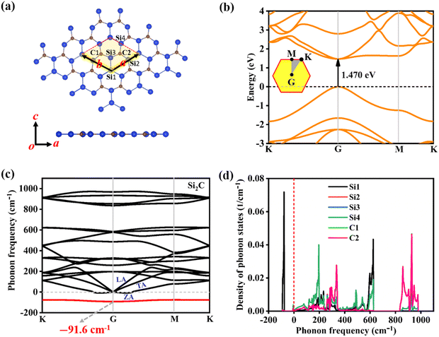 | ||
| Fig. 1 (a) Top/side view, (b) quasi-particle band structure, (c) phonon spectrum, and (d) density of phonon states of the optimized Si2C monolayer. | ||
In addition, the dynamical stability of the Si2C monolayer is examined by computing phonon dispersion, as presented in Fig. 1c. Three acoustic branches (ZA, TA, LA) and fifteen optical (O) branches of the Si2C monolayer are shown in Fig. 1c. The out-of-plane phonon mode (ZA) partially shifts to the negative frequency zone, with only a very small range near the G point. The maximum negative frequency is about −8.1 cm−1 along the G–M direction. Usually, negative frequencies less than −10 cm−1 can be neglected. However, a prominent optical phonon mode (marked by a red solid line) also falls in the negative frequency zone. The maximum imaginary frequency can be as large as about −91.6 cm−1 at the G point, indicating that the pristine Si2C monolayer is dynamically very unstable. Although a negative optical branch is found, the phonon frequencies of the highest four optical branches can reach values in the range of 800–1000 cm−1, suggesting a strong atom bond in the Si2C monolayer. Further, the calculated density of phonon states indicates that the imaginary optical phonon mode originates from the contribution of the Si1 atom (marked in Fig. 1a), as shown in Fig. 1d. The imaginary optical phonon mode could be directly related to the bonding nature around the Si1 atom, where Si–Si sp2-like hybridization is observed. Usually, Si–Si bonds in silicon materials are formed by sp3 hybridization (bulk silicon) or mixed sp2/sp3 hybridization (silicene).47 This suggests that the Si2C monolayer with Si–Si sp2-like hybridization is in a metastable state. The highest four optical modes are contributed by Si–C bonding. Although the Si2C monolayer has a desirable gap, structural stability is a prerequisite for the development of Si2C monolayer-based optoelectronic devices. Thus, the elimination of the imaginary optical phonon mode in the pristine Si2C monolayer should be considered first. Here, biaxial strain and surface functionalization are used to investigate the Si2C monolayer. The corresponding discussions are presented in Sections 3.2–3.4.
3.2 Strain effects on stability and electronic properties of the Si2C monolayer
Usually, biaxial compressive strain can easily induce an imaginary frequency in two-dimensional materials. Here, only the biaxial tensile strains are considered to investigate the dynamical stability of the Si2C monolayer. Fig. 2 exhibits the phonon spectra of the Si2C monolayer under biaxial tensile strains (δ) of +1 to +8%. The biaxial tensile strain δ can be realized by stretching the lattice constant, i.e. δ = (a1 − a)/a, where a1 and a are the lattice constants of the strained and pristine systems, respectively. With an increased δ, the maximum negative frequency in the Si2C monolayer can be decreased from −70.2 cm−1 (δ = +1%) to −34.7 cm−1 (δ = +2%) and the negative optical branch is slowly lifted up. When the tensile strain is as high as +2.5%, the imaginary frequency is eliminated fully, as shown in Fig. 2c. During the fabrication of the Si2C monolayer, a biaxial tensile strain of +2.5% can be generated when it is deposited on different substrates. When the tensile strain is further increased from +2.5% to +8%, no imaginary frequency is found in the Si2C monolayer and the highest four optical phonon modes are softened compared to the pristine structure, as seen in Fig. 2d–f. As a result, a relatively small biaxial tensile strain on the Si2C monolayer can significantly improve its dynamical stability.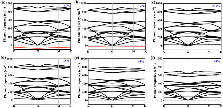 | ||
| Fig. 2 Phonon spectra of the Si2C monolayer under different tensile strains: (a) +1%, (b) +2%, (c) +2.5%, (d) +3%, (e) +5%, and (f) +8%. | ||
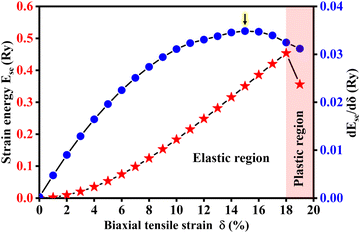
In fact, two-dimensional materials can withstand very large tensile strains before they are cracked.52 For example, graphene and silicene can reach fracture tensile strains of approximately +30% and +19% at room temperature,53,54 respectively. Thus, a wide tensile strain range of 0 to +19% is applied to the Si2C monolayer. The strain energy (Ese) in the Si2C monolayer is investigated first, as shown in Fig. 3 (red solid pentagrams). The critical tensile strain was observed at δ1 = +18%. Below the critical strain value, Ese constantly increases with an increased δ, followed by a parabolic shape, indicating that a hexagonal honeycomb configuration can be retained in the tensile strain range of 0 < δ < +18%. When the strain is higher than +18%, Ese suddenly decreases, indicating that the strained Si2C monolayer enters the plastic region (irreversible deformation) from the elastic region. In addition, the derivative curve of Ese with respect to δ is also depicted in Fig. 3 (blue solid circles). The first-order derivative dEse(δ)/dδ reaches a maximum value at δ2 = +15% (indicated by the black arrow in Fig. 3); then it slowly decreases when δ is further increased, indicating that the structure can be further expanded by a small tensile strain and becomes unstable. Fig. S1 of the ESI† shows the calculated phonon spectra of the Si2C monolayer at tensile strains of δ = +15% and +16%. The outstanding imaginary phonon frequencies at a tensile strain of +16% were observed, suggesting that the system remains in the metastable configuration in the tensile strain range of +15% < δ < +18%.
The second-order derivative of Ese is also calculated, which can throw light on the strength of the two-dimensional system. It is closely related to the in-plane stiffness (C). In the elastic strain range, C is defined via the expression55,56 , where So is the equilibrium surface area of the pristine Si2C monolayer. The in-plane stiffness of the Si2C monolayer is predicted to be about 135 N m−1, which is lower than those of the other honeycomb monolayers like SiC2 (393 N m−1),46 graphene (340 N m−1),21 and SiC (166 N m−1).55 However, it is much higher than that of silicene (62 N m−1) with a broad strain adjustment.55 The size of the in-plane stiffness in the Si2C monolayer indicates that it can be manipulated by strain engineering in the experiment, thus tuning the physical properties of the Si2C monolayer for use in different optoelectronic devices.
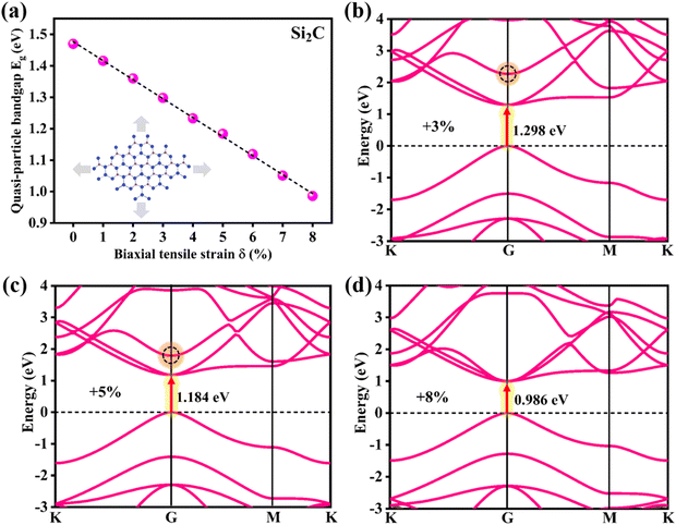
Fig. 4a displays the mutable quasi-particle energy bandgaps of the Si2C monolayer under different biaxial tensile strains of δ = 0 to +8%. With enhanced tensile strain, the quasi-particle bandgap decreased almost linearly from 1.470 eV (δ = 0) to 0.986 eV (δ = +8%) at the G0W0 level. The linear dependence of the quasi-particle bandgap on the strain originates from the deformation potential, i.e. the strain-induced band down-shifting.57,58 In fact, this phenomenon has also been reported previously for semiconducting silicon and germanium.59,60 The direct nature of the bandgap of the strained Si2C monolayer is retained in the observed strain range, as seen in Fig. 4b–d. Due to the increase of the tensile strain, the distance between the neighboring atoms becomes large, which directly leads to the reduction of the orbital overlap between the neighboring atoms, inducing a change of the orbital energy. The partial charge densities of the VBM and CBM of the Si2C monolayer are also exhibited under different strains (δ = 0, +3%, and +8%), as shown in Fig. S2 of the ESI.† It can be clearly seen that the CBM has been significantly influenced, while the VBM is almost unchanged. The remarkable charge change of the CBM can move the CBM down, thus reducing the bandgap of the Si2C monolayer with increasing tensile strain. It is also worth noting that the third conduction band at the G point is very sensitive to tensile strain, as indicated by the black dotted circle in Fig. 4b and c. When the strain is higher than +8%, the third conduction band becomes the CBM and the bandgap further decreases to zero at δ = +12% (as shown in Fig. S3 of the ESI†). The following discussion will focus on the optical properties of the Si2C monolayer under moderate tensile strains of 0 to +8% due to the suitable bandgap applied in optoelectronics.
3.3 Strain effects on the optical properties of the Si2C monolayer
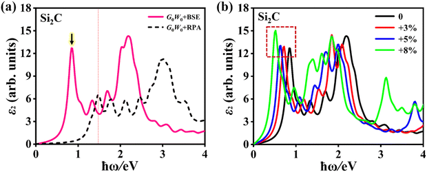
Compared with the bulk, atomically thin two-dimensional monolayers have significantly enhanced electron–electron (e–e) and electron–hole (e–h) couplings. At present, the G0W0 + BSE method has been regarded as an optimal method to obtain the exact optical properties of the monolayers, where the G0W0 and BSE methods can perform well with the e–e and e–h couplings, respectively. Based on the quasi-particle band structures, the incident light frequency-dependent dielectric constant ε (ω) of the Si2C monolayer can be obtained by solving the Bethe–Salpeter equation. ε (ω) is made up of the real part ε1 (ω) and imaginary part ε2 (ω), i.e., ε (ω) = ε1 (ω) + iε2 (ω). ε2 (ω) is referred to as the dissipation channel for the transition, which results in the optical absorption peaks, thus determining the optical absorption of the system. In addition, the depolarization effects in the 2D material are very significant for the incident polarized light vertical to the surface of the 2D material (i.e. the lattice vector c direction); that is the optical absorption for the in-plane polarized light is far greater than that of the out-of-plane polarized light. This was also verified in the Si2C monolayer, as shown in Fig. S4 of the ESI;† thus, only the optical properties were investigated for polarized light parallel to the surface (along the lattice vector a, as shown in Fig. 1a).Fig. 5a shows the ε2 (ω) of the pristine Si2C monolayer using the G0W0 + BSE and G0W0 + RPA methods along the lattice vector a. Compared with that of the G0W0 + RPA (excluding the e–h coupling), the optical spectrum from the G0W0 + BSE shows a significant red-shift, suggesting the importance of e–h coupling in the Si2C monolayer. It also exhibits a broad absorption range from near-infrared to near-ultraviolet light (0.5–4 eV). For a direct semiconductor, the first absorption peak is particularly meaningful. The position of the peak, i.e. the excitation energy Eee, is known as the optical gap of the system and can be measured experimentally. For the Si2C monolayer, the first absorption peak with a maximum oscillator of 1 is located at an energy of Eee = 0.849 eV (below the G0W0 bandgap Eg-G0W0 = 1.470 eV), corresponding to a bright bound exciton state. In light of the oscillator strength selection rule, the first absorption peak is confirmed to originate from the VBM → CBM vertical transition at the G point. Thus, the binding energy (Eeb) of the bright bound exciton is predicted to be 0.621 eV by the energy difference between Eg-G0W0 and the excitation energy Eee, i.e. Eeb = Eg-G0W0 − Eee. Such a significant binding energy of excitons is useful for effectively confining both photogenerated electrons and holes, greatly slowing down their recombination, thus increasing the light utilization efficiency. This is a very huge advantage compared to that of the semiconducting bulk (less than 50 meV)49,61,62.
Next, the strain-dependent optical properties of the Si2C monolayer are also evaluated for potential application in optoelectronics. Fig. 5b shows the ε2 of the Si2C monolayer in the biaxial tensile strain range of 0 < δ < +8%, in which the first absorption peak is found at 0. 849 eV, 0.713 eV, 0.628 eV, 0.511 eV for tensile strains δ = 0, +3%, +5%, and +8%, respectively. The first absorption peak is dramatically red-shifted by approximately 0.338 eV under a tensile strain of +8%. Such a red-shift of the absorption curve causes a significant enhancement for near-infrared light, which should be attributed to the decreased bandgap. The first absorption peaks in the strained systems are formed by the VBM–CBM vertical transition at the G point. The binding energies of the bright bound excitons corresponding to the first absorption peaks are also calculated to be 0.585 eV (δ = +3%), 0.556 eV (δ = +5%), and 0.475 eV (δ = +8%), as listed in Table 1. The estimated Eeb is reduced by 146 meV from 0.621 eV (δ = 0) to 0.475 (δ = +8%), indicating that Eeb can be tuned by the tensile strains and first bright bound exciton still has high stability at a large tensile strain of +8%.
| Strain | E ee | E g-G0W0 | E eb | R er |
|---|---|---|---|---|
| 0 | 0.849 | 1.470 | 0.621 | 31.36 |
| +3% | 0.713 | 1.298 | 0.585 | 33.47 |
| +5% | 0.626 | 1.184 | 0.556 | 36.25 |
| +8% | 0.511 | 0.986 | 0.475 | 43.51 |
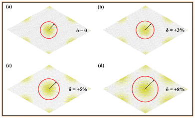
Further, these bright bound excitons in the strained Si2C monolayer are also investigated. The normalized squared exciton wave function |ψ(re,rh)|2 is obtained by  , where re and rh are the real-space electron and hole coordinates, respectively. The calculated hole (red solid sphere) is located at the center of a supercell with dimensions 30 × 30 × 1. Fig. 6 presents the real-space distribution of the electron. It can be clearly seen that the bright bound exciton in the pristine Si2C monolayer is more spatially localized than those in the strained Si2C monolayer. The estimated exciton radii (Rer) are about 31.36 Å, 33.47 Å, 36.25 Å, and 43.51 Å for δ = 0, +3%, +5%, and +8%, respectively. This indicates that a larger binding energy of an exciton can induce a smaller extended electron distribution in real space; thus, a weaker electronic screening is found in a smaller, strained system. This also suggests that the electron–hole pairs in the relatively large strain are easier to separate. As a result, the separated electrons and holes in the strained Si2C monolayer could be applied to improve the performance of optoelectronic devices based on the Si2C monolayer.
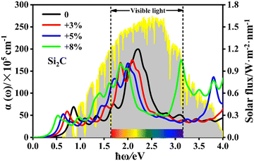
To further exhibit the light-harvesting ability of the Si2C monolayer for the sunlight under the biaxial tensile strain, the light absorption coefficient is also calculated by the following equation:63
 | (2) |
3.4 Fluorination effects on stable, electronic and optical properties
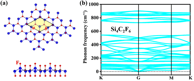
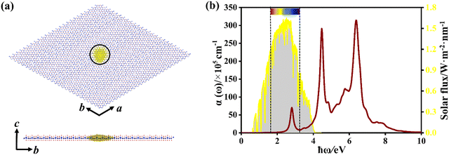
The optimized configuration of the fully fluorinated Si2C monolayer (Si4C2F6) is shown in Fig. 8a, where the lattice constant a/b is 5.829 Å and lSi–Si (lSi–C) is 2.356 (1.928) Å. These lattice parameters are higher than those of pristine Si2C monolayer. Due to full fluorination, the planar configuration was transformed to the buckled configuration. The buckled Si4C2F6 is similar to previously reported fluorinated silicene and fluorinated graphene.47 The Si–F and C–F bond lengths are predicted to be about 1.611 Å and 1.456 Å, respectively, which are very close to those in fluorinated silicene and fluorinated graphene (1.620 Å; 1.390 Å).47 Although Si4C2F6 is a buckling structure, the hexagonal lattice is still retained. Compared to the pristine Si2C monolayer, the different lattice parameters of Si4C2F6 can cause different phonon dispersions and band structures. Fig. 8b exhibits the calculated phonon spectrum of Si4C2F6, in which the negative frequencies induced by the Si1 atom in the pristine Si2C monolayer were eliminated by fluorination. This indicates that Si4C2F6 is dynamically stable, suggesting that fluorination is an effective way to enhance the dynamical stability of the Si2C monolayers.Fig. 9a shows the quasi-particle band structure of Si4C2F6, in which it is still a direct-gap semiconductor at the G point. The estimated gap is 3.739 eV, which is much larger than that of the pristine Si2C monolayer (1.470 eV). It is between 7.010 eV for fluorinated graphene and 2.760 eV for fluorinated silicene.47 Such a large gap can induce large absorption of incident near-ultraviolet light, as shown in Fig. 9b. Compared with that of the pristine Si2C monolayer, the optical spectrum of Si4C2F6 was blue-shifted significantly due to the large electronic bandgap. The first absorption peak is located at 2.806 eV, and originates from the VBM → CBM vertical transition; thus, a bright bound exciton is formed. The exciton binding energy was estimated to be 0.933 eV, which is significantly higher than that of the pristine Si2C monolayer (0.621 eV). This can induce a relative localization of electrons, thus resulting in a small exciton radius of 11.03 Å, as shown in Fig. 10a. In addition, the absorption coefficient can attain a value of 107 cm−1 for near-ultraviolet light, as seen in Fig. 10b. These results indicate that Si4C2F6 can be used in optoelectronic devices based on wide-gap semiconductors like ultraviolet photodetectors and sensors.
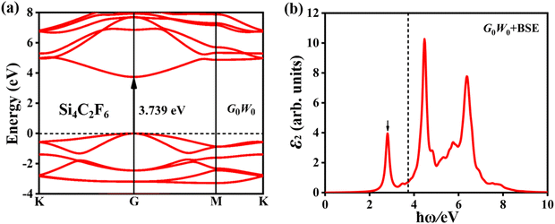 | ||
| Fig. 9 (a) Quasi-particle band structure and (b) imaginary part (ε2) of the dielectric function of Si4C2F6. The dashed line indicates the position corresponding to the quasi-particle bandgap. | ||
4 Conclusions
In conclusion, the structural stability, quasi-particle band structures, and optical properties of Si2C monolayers were systematically investigated under tensile strain and fluorination. The pristine Si2C monolayer had a moderate in-plane stiffness of 135 N m−1, ensuring that it could be manipulated experimentally by strain engineering. A biaxial tensile strain between +2.5% and +15% can maintain the dynamical stability of the structure. The quasi-particle bandgap of the Si2C monolayer at the G0W0 level could be linearly tuned from 1.470 eV (δ = 0) to 0.986 eV (δ = +8%), even becoming a semimetal at a tensile strain of +12%. The increased tensile strain leads to a significant red-shift of the optical absorption spectrum, thus enhancing the absorption for the near-infrared light. The pristine Si2C monolayer had a large exciton binding energy of 0.621 eV, suggesting that the photogenerated electrons and holes could not be easily recombined by external perturbations. More importantly, when the tensile strain is increased to +8%, the binding energy of the bright bound exciton corresponding to the first absorption peak only decreased by 146 meV, indicating that the observed exciton is still stable in the relatively large tensile strain range. In addition, fluorination can cause a large quasi-particle bandgap of 3.739 eV with direct characteristics and a considerable exciton binding energy of 0.933 eV in the Si2C monolayer. These results are very important for the application of Si2C monolayers in nanoelectronic and optoelectronic devices.Conflicts of interest
There are no conflicts to declare.Acknowledgements
The authors gratefully acknowledge financial support from the Jiangsu University of Science and Technology (No. 1052931610).References
- K. I. Bolotin, K. J. Sikes, Z. Jiang, M. Klima, G. Fudenberg, J. Hone, P. Kim and H. L. Stormer, Solid State Commun., 2008, 146, 351–355 CrossRef CAS.
- T. J. Booth, P. Blake, R. R. Nair, D. Jiang, E. W. Hill, U. Bangert, A. Bleloch, M. Gass, K. S. Novoselov, M. I. Katsnelson and A. K. Geim, Nano Lett., 2008, 8, 2442–2446 CrossRef CAS PubMed.
- M. Liu, X. Yin, E. Ulin-Avila, B. Geng, T. Zentgraf, L. Ju, F. Wang and X. Zhang, Nature, 2011, 474, 64–67 CrossRef CAS PubMed.
- H. Shu, J. Mater. Sci., 2021, 56, 5684–5696 CrossRef CAS.
- L. C. Lew Yan Voon, J. Zhu and U. Schwingenschlögl, Appl. Phys. Rev., 2016, 3, 040802 Search PubMed.
- B. D. Hoi, M. Yarmohammadi and H. A. Kazzaz, J. Magn. Magn. Mater., 2017, 439, 203–212 CrossRef CAS.
- M. Yarmohammadi, RSC Adv., 2017, 7, 10650–10659 RSC.
- D. Z. Jakovljević, M. M. Grujić, M. Ž. Tadić and F. M. Peeters, J. Phys.: Condens. Matter, 2017, 30, 035301 CrossRef PubMed.
- M. Yarmohammadi, J. Magn. Magn. Mater., 2017, 426, 621–628 CrossRef CAS.
- H. C. Hsueh, G. Y. Guo and S. G. Louie, Phys. Rev. B: Condens. Matter Mater. Phys., 2011, 84, 085404 CrossRef.
- L.-J. Zhou, Y.-F. Zhang and L.-M. Wu, Nano Lett., 2013, 13, 5431–5436 CrossRef CAS PubMed.
- M. Zhao and R. Zhang, Phys. Rev. B: Condens. Matter Mater. Phys., 2014, 89, 195427 CrossRef.
- H. Dong, L. Wang, L. Zhou, T. Hou and Y. Li, Carbon, 2017, 113, 114–121 CrossRef CAS.
- X. Liu, X. Shao, B. Yang and M. Zhao, Nanoscale, 2018, 10, 2108–2114 RSC.
- H. Dong, L. Zhou, T. Frauenheim, T. Hou, S.-T. Lee and Y. Li, Nanoscale, 2016, 8, 6994–6999 RSC.
- S. Lin, S. Zhang, X. Li, W. Xu, X. Pi, X. Liu, F. Wang, H. Wu and H. Chen, J. Phys. Chem. C, 2015, 119, 19772–19779 CrossRef CAS.
- C. M. Polley, H. Fedderwitz, T. Balasubramanian, A. A. Zakharov, R. Yakimova, O. Bäcke, J. Ekman, S. P. Dash, S. Kubatkin and S. Lara-Avila, Phys. Rev. Lett., 2023, 130, 076203 CrossRef CAS PubMed.
- G. G. Naumis, S. Barraza-Lopez, M. Oliva-Leyva and H. Terrones, Rep. Prog. Phys., 2017, 80, 096501 CrossRef PubMed.
- C. Si, Z. Sun and F. Liu, Nanoscale, 2016, 8, 3207–3217 RSC.
- J. Du, H. Yu, B. Liu, M. Hong, Q. Liao, Z. Zhang and Y. Zhang, Small Methods, 2021, 5, 2000919 CrossRef CAS PubMed.
- C. Lee, X. Wei, J. W. Kysar and J. Hone, Science, 2008, 321, 385–388 CrossRef CAS PubMed.
- B. Mortazavi, O. Rahaman, M. Makaremi, A. Dianat, G. Cuniberti and T. Rabczuk, Phys. E, 2017, 87, 228–232 CrossRef CAS.
- S. Bertolazzi, J. Brivio and A. Kis, ACS Nano, 2011, 5, 9703–9709 CrossRef CAS PubMed.
- Q. Wei and X. Peng, Appl. Phys. Lett., 2014, 104, 251915 CrossRef.
- S. Wang, M. S. Ukhtary and R. Saito, Phys. Rev. Res., 2020, 2, 033340 CrossRef CAS.
- S. Wang, H. Tian and M. Sun, J. Phys.: Condens. Matter, 2023, 35, 304002 CrossRef PubMed.
- A. Azizi, X. Zou, P. Ercius, Z. Zhang, A. L. Elías, N. Perea-López, G. Stone, M. Terrones, B. I. Yakobson and N. Alem, Nat. Commun., 2014, 5, 4867 CrossRef CAS PubMed.
- G. Tsoukleri, J. Parthenios, K. Papagelis, R. Jalil, A. C. Ferrari, A. K. Geim, K. S. Novoselov and C. Galiotis, Small, 2009, 5, 2397–2402 CrossRef CAS PubMed.
- F. Ding, H. Ji, Y. Chen, A. Herklotz, K. Dörr, Y. Mei, A. Rastelli and O. G. Schmidt, Nano Lett., 2010, 10, 3453–3458 CrossRef CAS PubMed.
- K. Cao, S. Feng, Y. Han, L. Gao, T. Hue Ly, Z. Xu and Y. Lu, Nat. Commun., 2020, 11, 284 CrossRef CAS PubMed.
- X. Tang, T. Fan, C. Wang and H. Zhang, Small, 2021, 17, 2005640 CrossRef CAS PubMed.
- W. Feng, P. Long, Y. Feng and Y. Li, Adv. Sci., 2016, 3, 1500413 CrossRef PubMed.
- X. Chen, K. Fan, Y. Liu, Y. Li, X. Liu, W. Feng and X. Wang, Adv. Mater., 2022, 34, 2101665 CrossRef CAS PubMed.
- N. Liu, G. Bo, Y. Liu, X. Xu, Y. Du and S. X. Dou, Small, 2019, 15, 1805147 CrossRef PubMed.
- T. Hartman, J. Šturala, J. Luxa and Z. Sofer, ACS Nano, 2020, 14, 7319–7327 CrossRef CAS PubMed.
- P. Giannozzi, S. Baroni, N. Bonini, M. Calandra, R. Car, C. Cavazzoni, D. Ceresoli, G. L. Chiarotti, M. Cococcioni, I. Dabo, A. Dal Corso, S. de Gironcoli, S. Fabris, G. Fratesi, R. Gebauer, U. Gerstmann, C. Gougoussis, A. Kokalj, M. Lazzeri, L. Martin-Samos, N. Marzari, F. Mauri, R. Mazzarello, S. Paolini, A. Pasquarello, L. Paulatto, C. Sbraccia, S. Scandolo, G. Sclauzero, A. P. Seitsonen, A. Smogunov, P. Umari and R. M. Wentzcovitch, J. Phys.: Condens. Matter, 2009, 21, 395502 CrossRef PubMed.
- A. Marini, C. Hogan, M. Grüning and D. Varsano, Comput. Phys. Commun., 2009, 180, 1392–1403 CrossRef CAS.
- J. P. Perdew, K. Burke and M. Ernzerhof, Phys. Rev. Lett., 1996, 77, 3865–3868 CrossRef CAS PubMed.
- N. Troullier and J. L. Martins, Phys. Rev. B: Condens. Matter Mater. Phys., 1991, 43, 1993 CrossRef CAS PubMed.
- S. Baroni, S. de Gironcoli, A. Dal Corso and P. Giannozzi, Rev. Mod. Phys., 2001, 73, 515–562 CrossRef CAS.
- L. Hedin, Phys. Rev., 1965, 139, A796–A823 CrossRef.
- M. S. Hybertsen and S. G. Louie, Phys. Rev. B: Condens. Matter Mater. Phys., 1986, 34, 5390 CrossRef CAS PubMed.
- A. L. Fetter and J. D. Walecka, Quantum Theory of Many-Particle Systems, Dover, New York, 2003, ch. 15, p. 565 Search PubMed.
- E. E. Salpeter and H. A. Bethe, Phys. Rev., 1951, 84, 1232 CrossRef.
- G. Onida, L. Reining and A. Rubio, Rev. Mod. Phys., 2002, 74, 601–659 CrossRef CAS.
- H. Shu, Appl. Surf. Sci., 2021, 559, 149956 CrossRef CAS.
- W. Wei and T. Jacob, Phys. Rev. B: Condens. Matter Mater. Phys., 2013, 88, 045203 CrossRef.
- H. Shu, Phys. Chem. Chem. Phys., 2023, 25, 7937–7945 RSC.
- V. Tran, R. Soklaski, Y. Liang and L. Yang, Phys. Rev. B: Condens. Matter Mater. Phys., 2014, 89, 235319 CrossRef.
- H. Shu, Y. Li, X. Niu and J. Wang, Phys. Chem. Chem. Phys., 2016, 18, 6085–6091 RSC.
- A. Ramasubramaniam, Phys. Rev. B: Condens. Matter Mater. Phys., 2012, 86, 115409 CrossRef.
- J. Annett and G. L. W. Cross, Nature, 2016, 535, 271–275 CrossRef CAS PubMed.
- Q. X. Pei, Y. W. Zhang and V. B. Shenoy, Carbon, 2010, 48, 898–904 CrossRef CAS.
- Q.-X. Pei, Z.-D. Sha, Y.-Y. Zhang and Y.-W. Zhang, J. Appl. Phys., 2014, 115, 023519 CrossRef.
- H. Şahin, S. Cahangirov, M. Topsakal, E. Bekaroglu, E. Akturk, R. T. Senger and S. Ciraci, Phys. Rev. B: Condens. Matter Mater. Phys., 2009, 80, 155453 CrossRef.
- M. Topsakal, S. Cahangirov and S. Ciraci, Appl. Phys. Lett., 2010, 96, 091912 CrossRef.
- C. G. Van de Walle, Phys. Rev. B: Condens. Matter Mater. Phys., 1989, 39, 1871–1883 CrossRef CAS PubMed.
- Z. Liu, J. Wu, W. Duan, M. G. Lagally and F. Liu, Phys. Rev. Lett., 2010, 105, 016802 CrossRef PubMed.
- M. V. Fischetti and S. E. Laux, J. Appl. Phys., 1996, 80, 2234–2252 CrossRef CAS.
- D. Yu, Y. Zhang and F. Liu, Phys. Rev. B: Condens. Matter Mater. Phys., 2008, 78, 245204 CrossRef.
- W. Shan, B. D. Little, A. J. Fischer, J. J. Song, B. Goldenberg, W. G. Perry, M. D. Bremser and R. F. Davis, Phys. Rev. B: Condens. Matter Mater. Phys., 1996, 54, 16369–16372 CrossRef CAS PubMed.
- T. Cheiwchanchamnangij and W. R. L. Lambrecht, Phys. Rev. B: Condens. Matter Mater. Phys., 2012, 85, 205302 CrossRef.
- X. Liu, P. Gao, W. Hu and J. Yang, J. Phys. Chem. Lett., 2020, 11, 4070–4079 CrossRef CAS PubMed.
- X. Zhu, F. Li, Y. Wang, M. Qiao and Y. Li, J. Mater. Chem. C, 2018, 6, 4494–4500 RSC.
- M. Kar, R. Sarkar, S. Pal and P. Sarkar, Phys. Rev. B, 2020, 101, 195305 CrossRef CAS.
- A. Bafekry, M. Faraji, D. M. Hoat, M. Shahrokhi, M. M. Fadlallah, F. Shojaei, S. A. H. Feghhi, M. Ghergherehchi and D. Gogova, J. Phys. D: Appl. Phys., 2021, 54, 155303 CrossRef CAS.
Footnote |
| † Electronic supplementary information (ESI) available. See DOI: https://doi.org/10.1039/d4tc00401a |
| This journal is © The Royal Society of Chemistry 2024 |

