
 Open Access Article
 This Open Access Article is licensed under a Creative Commons Attribution-Non Commercial 3.0 Unported Licence
Enhancing the stability of inverted perovskite solar cells through Cu2ZnSnS4 nanoparticles hole transporting material†
Elisa
Fabbretti
a,
Amin Hasan
Husien
a,
Rahul
Patidar
 b,
Karen
Valadez-Villalobos
b,
James
McGettrick
b,
Andreia
Amighini Alerhush
a,
Ershad
Parvazian
b,
Matthew L.
Davies
b,
Trystan
Watson
b,
Alessandro
Minotto
a,
Giorgio
Tseberlidis
a,
Adele
Sassella
a,
Vanira
Trifiletti
*a and
Simona
Binetti
a
b,
Karen
Valadez-Villalobos
b,
James
McGettrick
b,
Andreia
Amighini Alerhush
a,
Ershad
Parvazian
b,
Matthew L.
Davies
b,
Trystan
Watson
b,
Alessandro
Minotto
a,
Giorgio
Tseberlidis
a,
Adele
Sassella
a,
Vanira
Trifiletti
*a and
Simona
Binetti
a
aDepartment of Materials Science and Solar Energy Research Centre (MIB-SOLAR), University of Milano-Bicocca, Via Cozzi 55, 20126, Milan, Italy. E-mail: vanira.trifiletti@unimib.it
bSPECIFIC IKC, Faculty of Science and Engineering, Swansea University, Fabian Way, Swansea, SA1 8EN, UK
First published on 9th January 2025
Abstract
Perovskite solar cells (PSCs) have burst into photovoltaic (PV) research, revolutionising it and demonstrating that they can achieve performances comparable to technologies already on the market. Despite that, the major limitation of PSCs' commercialisation is their poor environmental stability. Inorganic carriers transporting materials have gained attention for enhancing PSCs' durability due to their superior stability and non-hygroscopic nature. Among them, kesterite Cu2ZnSnS4 (CZTS) is a promising inorganic hole transporting material (HTM) thanks to its optimal electronic properties, non-toxic, abundant elements, and simple solution deposition methods. Herein, the effect on the stability of inverted PSCs employing CZTS nanoparticles (NPs) as HTM is investigated by X-ray photoelectron and ultraviolet photoelectron spectroscopy, together with steady-state and time-resolved photoluminescence spectroscopies. Special attention was given to the alteration in the PV performances over time of the CZTS-based device compared to a control device with a common organic HTM. The enhanced stability of the CZTS NPs-based devices in opposition to degradation of the devices with a [2-(3,6-dimethoxy-9H-carbazol-9-yl)ethyl]phosphonic acid (MeO-2PACz) self-assembled monolayer as HTM was demonstrated through solar simulator measurements and external quantum efficiency. The efficiency of a CZTS-based p–i–n PSC increased by 34% after three weeks, while the efficiency of the organic HTM-based device decreased by 16% during the same period. Furthermore, CZTS-based PSCs showed a drop-in efficiency of 80% after four days under a humidity test at 70% RH, while the efficiency of the organic HTM-based devices dropped by 80% after two days under the same conditions. Moreover, analysis of the photoluminescence spectra reveals no modification of the CZTS-based PSCs.
1. Introduction
The relentless progression of climate change prompted the United Nations to set a new target for achieving a climate-neutral world by the mid-21st century. This means maximum reduction in greenhouse gas emissions until they are equal to or lower than those naturally absorbed by the planet to achieve a net-zero emissions balance by 2050.1,2 This is necessary to comply with the provisions of the Paris Agreement to limit the temperature rise to 1.5 °C above pre-industrial levels.3,4 At present 73.2% of global greenhouse gases come from energy production from fossil fuels.5 Therefore, urgent and decisive action to transition towards sustainable energy solutions is required. The European Union (EU) has demonstrated a strong commitment to this transition through its European Green Deal, aiming for climate neutrality by 2050.6 Solar photovoltaic (PV) technology stands out due to its vast potential for decarbonised and inexhaustible energy production. In addition, given its scalability and declining cost, solar PV is poised to play a crucial role in meeting the EU objectives.7 In this context, emerging thin-film perovskite-based PV technology has garnered significant attention thanks to its impressive performance. The power conversion efficiency (PCE) of perovskite solar cells (PSCs) swiftly increased from about 4% in 2009 to over 26% in recent laboratory settings.8 This rapid advancement is largely due to the unique properties of metal halide perovskite materials, such as their high absorption coefficients (105–106 cm−1), tuneable direct bandgap (from 1.1 eV to 2.0 eV), high carrier mobility (tens of cm2 V−1 s−1),9 and long carrier diffusion lengths.10 These properties enable efficient light absorption and charge transport, making PSCs highly competitive with other PV technologies. Moreover, the simple solution-based fabrication of PSCs offers several advantages, including low costs for raw materials and manufacturing, scalability, and the ability to use flexible substrates. This process involves depositing a series of layers: a transparent conducting oxide (TCO) on a glass substrate, a hole transport material (HTM), the perovskite light-absorbing layer, an electron transport material (ETM), and a metal back contact. The device architectures are defined by the first layer deposited on the substrate: when the n-type semiconductor is the first on the TCO, the architecture is called conventional and identified as n–i–p.11–13 On the other hand, PSCs in p–i–n architecture, also known as inverted architecture, are increasingly favoured due to their numerous advantages such as enhanced stability and ease of fabrication.14,15 Additionally, the p–i–n structure facilitates efficient charge collection, resulting in higher open-circuit voltages and improved device performances.16,17 Also, the ability to process all the layers at sub 150 °C opens up the possibility of low-cost, high throughput manufacturing methods such as roll-to-roll manufacturing.18,19 Despite the impressive advancements, several challenges concerning stability remain in the commercial deployment of PSCs. The primary factors causing irreversible degradation of the perovskite photo-absorbing layer include continuous exposure to bias voltage, prolonged exposure to illumination and heat, and moisture.8,20–23 Among these degradation mechanisms, degradation due to humidity is the most detrimental one since metal halide perovskite consists of hygroscopic organic cations, such as methylammonium (MA, CH3NH3+) and formamidinium (FA, CH(NH2)2+), metal cations as lead (Pb2+) and tin (Sn2+), and halide anions, typically iodine (I−), bromine (Br−), and chlorine (Cl−).24,25 When water molecules come in contact with the perovskite, reactions to form photoinactive phases occur, generating mainly lead halides and oxides.24,25 This issue is being tackled from two angles. First, researchers are developing various strategies to prevent moisture from reaching the perovskite layer, such as using encapsulants and improving the inner layers of PSCs.26,27 Second, efforts are focused on enhancing the inherent stability of PSCs in the presence of moisture.28,29 In the latter case, one attractive way is to employ inorganic carriers transporting materials which offer superior stability, easier synthesis, and lower cost compared to the commercial organic alternatives.21,30–32 Cu2ZnSnS4 nanoparticles (CZTS NPs) emerged as a promising inorganic HTM due to their earth-abundant, non-toxic nature and excellent electronic properties, such as high hole mobility (∼35 cm2 V−1 s−1).33–35 Thanks to these features, kesterite has been largely employed as absorber material in thin-film solar cells to substitute Cu(In,Ga)(S,Se)2 and CdTe thin-film solar cells, constituted by rare and toxic elements.36–39 However, kesterite PV technology has always shown PCE values lower than CIGS and CdTe solar cells.40 Furthermore, using CZTS NPs as an absorber layer in solar cells does not work due to the excessive presence of grain boundaries.41 However, they have been explored as charge extractors in PSCs,42,43 and recently as electro/photo-catalysts.44,45 The employment of CZTS NPs as HTM has proved its worth since 2015 when Wu and colleagues reached a PCE of 12.8% with a conventional PSC architecture.43 The NPs were dispersed in 1-hexanediol and deposited by spin coating; the perovskite used was the methylammonium lead iodide (CH3NH3PbI3, MAPbI3). In 2016, Khanzada and colleagues obtained the record PCE of 15.4% with an inverted architecture and MAPbI3 as perovskite.46 The NPs layer was obtained by depositing a solution of ligand-stripped CZTS NPs in N-dimethylformamide (DMF) through spin coating. In 2018, Zuo and colleagues reached a PCE of 13.4% in n–i–p MAPbI3 PSCs using a wurtzite CZTS NPs HTM.47 In 2019, Ashebir and colleagues prepared CZTS NPs compact films in situ on glass/ITO substrates by spin coating a novel molecular precursor solution.48 In this way, they could better control the HTM's thickness, achieving a PCE of 6.0% with a 97 nm thick NPs layer. The device had an inverted architecture, and the perovskite was again the MAPbI3. Although CZTS NPs are employed as HTM due to low-cost precursors, simple deposition methods and the stability they can give to PSCs, few articles in the literature show the effect on PSCs stability. Additionally, stability was always investigated over a small period of time. This is the case of Ashebir and colleagues; they showed that a CZTS NPs-based device, made as mentioned above, was able to retain 87% of its efficiency after 43 days stored in N2 atmosphere.48 Their control device, a p–i–n PSC with PEDOT:PSS as HTM, almost degraded after 35 days of storing. Another work showing the better stability of PSC given by CZTS NPs is the work of Patel and colleagues.49 They obtained a n–i–p PSC (CH3NH3Pb1−xSnxI3−yCly) with CZTS NPs as HTM that outperformed the organic counterpart (Spiro-OMeTAD) by retaining the 75% of its initial efficiency (9.7%) after 168 h. Then, both the devices started to degrade at a similar rate.This study explores the integration of CZTS NPs as an innovative HTM to increase the stability of inverted PSCs. The surface composition of CZTS NPs layers annealed at three different temperatures (350 °C, 300 °C, and 250 °C) was analysed. These layers were then incorporated into p–i–n PSCs to determine the optimal annealing temperature. Once optimised, CZTS NPs-based devices were compared to control p–i–n PSCs with the commercial self-assembled monolayer (SAM) of [2-(3,6-dimethoxy-9H-carbazol-9-yl)ethyl]phosphonic acid (MeO-2PACz) as HTM. The introduction of CZTS NPs as an HTM showed promising results. The optimised CZTS NPs-based PSCs exhibited significant improvements in operational stability compared to the control devices using SAM as HTM. The CZTS NPs-based device demonstrated an increase in efficiency from 4.71% of the first measurement to 6.04% after 18 weeks. Meanwhile, for the SAM-based device, the efficiency decreased from 12.07%, the best value obtained one week after the first measurement, to 6.87% in 18 weeks. This improvement in PCE over time was further investigated and found to result from enhanced charge injection from the MAPbI3 to the CZTS NPs layer. This suggests the interface between these two layers improves over time, enhancing overall performance.
2. Experimental details
2.1 Materials
Sulphur powder (>99.5%); copper(II) acetate monohydrate (Cu(CH3COO)2·H2O, >99%); zinc(II) acetate dihydrate (Zn(CH3COO)2·2H2O, 99.99%); tin(II) chloride dihydrate (SnCl2·2H2O, >98%); oleylamine (CH3(CH2)7CH![[double bond, length as m-dash]](https://www.rsc.org/images/entities/char_e001.gif) CH(CH2)7CH2NH2, 98%); p-xylene (>99.7%); and terpineol (mixture of isomers) were purchased from Sigma-Aldrich (St. Louis, MO, USA). Ethyl cellulose (ethoxy content 48%, 22 cps) was purchased from Thermo Fisher Scientific (Waltham, MA, USA). Lead(II) iodide (PbI2, 99.99%) was purchased from TCI (trace metals basis, Tokyo, Japan). Methylammonium iodide (CH3NH3I, MAI, 99.99%) was purchased from Greatcell Solar Materials (Australia). Methylamine (ca. 9% in acetonitrile, CH3NH2 in CH3CN, MA in ACN) was purchased from TCI (Tokyo Chemical Industry UK Ltd). Anhydrous acetonitrile (CH3CN, ACN, ≥99.9%) was purchased from Fisher Scientific (part of Thermo Fisher Scientific, UK). Hydrochloric acid (HCl, 37%) was purchased from Sigma-Aldrich (St. Louis, MO, USA). MeO-2PACz ([2-(3,6-dimethoxy-9H-carbazol-9-yl)ethyl]phosphonic acid, C16H18NO5P, ≥98.0%) was purchased from TCI (Tokyo Chemical Industry UK Ltd). Extra dry 2-propanol ((CH3)2CHOH, IPA, 99.8%) was purchased from Fisher Scientific (part of Thermo Fisher Scientific, UK). [6,6]-Phenyl C61 butyric acid methyl ester (C72H14O2, PC61BM) was purchased from 1-Material Inc. (Canada). Anhydrous chlorobenzene (C6H5Cl, CB, 99.8%) was purchased from Sigma-Aldrich (Germany). Bathocuproine (C26H20N2, BCP) was purchased from TCI (Tokyo Chemical Industry UK Ltd). Anhydrous ethanol (CH3CH2OH, EtOH) was purchased from Thermo Fisher (UK). Silver (Ag) pellets (99.99%) were purchased from Kurt J. Lesker Co. (US). Pre-patterned 15 ohm per sq. glass/ITO substrates (28 × 28 × 1.1 mm) were purchased from Kintec Co. (Hong Kong).
CH(CH2)7CH2NH2, 98%); p-xylene (>99.7%); and terpineol (mixture of isomers) were purchased from Sigma-Aldrich (St. Louis, MO, USA). Ethyl cellulose (ethoxy content 48%, 22 cps) was purchased from Thermo Fisher Scientific (Waltham, MA, USA). Lead(II) iodide (PbI2, 99.99%) was purchased from TCI (trace metals basis, Tokyo, Japan). Methylammonium iodide (CH3NH3I, MAI, 99.99%) was purchased from Greatcell Solar Materials (Australia). Methylamine (ca. 9% in acetonitrile, CH3NH2 in CH3CN, MA in ACN) was purchased from TCI (Tokyo Chemical Industry UK Ltd). Anhydrous acetonitrile (CH3CN, ACN, ≥99.9%) was purchased from Fisher Scientific (part of Thermo Fisher Scientific, UK). Hydrochloric acid (HCl, 37%) was purchased from Sigma-Aldrich (St. Louis, MO, USA). MeO-2PACz ([2-(3,6-dimethoxy-9H-carbazol-9-yl)ethyl]phosphonic acid, C16H18NO5P, ≥98.0%) was purchased from TCI (Tokyo Chemical Industry UK Ltd). Extra dry 2-propanol ((CH3)2CHOH, IPA, 99.8%) was purchased from Fisher Scientific (part of Thermo Fisher Scientific, UK). [6,6]-Phenyl C61 butyric acid methyl ester (C72H14O2, PC61BM) was purchased from 1-Material Inc. (Canada). Anhydrous chlorobenzene (C6H5Cl, CB, 99.8%) was purchased from Sigma-Aldrich (Germany). Bathocuproine (C26H20N2, BCP) was purchased from TCI (Tokyo Chemical Industry UK Ltd). Anhydrous ethanol (CH3CH2OH, EtOH) was purchased from Thermo Fisher (UK). Silver (Ag) pellets (99.99%) were purchased from Kurt J. Lesker Co. (US). Pre-patterned 15 ohm per sq. glass/ITO substrates (28 × 28 × 1.1 mm) were purchased from Kintec Co. (Hong Kong).
2.2 Synthesis of CZTS NPs
CZTS NPs were synthesised by hot injection technique, using a method well-described elsewhere in the literature with minor changes.46,50 The synthesis process begins with the preparation of two solutions. One solution, containing all metal precursor (Sol-M), was obtained by dissolving in 15 mL of oleylamine the reactants in the following order: 959.30 mg Cu (CH3COO)2·H2O, 625.40 mg SnCl2·2H2O, and 628.90 mg Zn (CH3COO)2·2H2O. The other solution was prepared by introducing 312 mg of sulphur powder in 10 mL of oleylamine (Sol-S). The two mixtures were prepared in two different three-neck flasks, put in heating mantles and connected to a vacuum/N2 Schlenk line. Sol-S was warmed at 60 °C and degassed for 1 hour under constant stirring. Sol-M underwent a three-step temperature process: (i) degassing at 100 °C under powerful stirring for 1 hour to extract dissolved oxygen and unwanted moisture; (ii) refilling of the flask with N2 while rising slowly the temperature to the injection temperature of 180 °C, during this step the solution colour turned from bluish to yellowish; (iii) rapid injection of Sol-S into Sol-M after the changes in the Sol-M colour, leading to a further quick colour variation from pale yellow to dark brown. After the injection, the temperature increased to 280 °C, and the solution was left to react for 30 minutes. Then, the heating mantle was removed, and the flask was let to cool down to room temperature in an inert atmosphere. The final suspension was washed with a mixture of chloroform and ethanol in a 1![[thin space (1/6-em)]](https://www.rsc.org/images/entities/char_2009.gif) :5 (v/v) ratio and centrifuged at 8000 rpm for 2 minutes. The supernatant was removed, and the washing procedure was repeated several times to remove the exceeding residues of oleylamine from the CZTS NPs surface, which may limit the particle-to-particle interactions and reduce the charge carrier in the HTM film. Then, the CZTS NPs were collected, dried under a vacuum and stored under an N2 atmosphere. In our recently published studies, it has been demonstrated that the synthesis temperature of CZTS NPs is of fundamental importance for the correct formation of the kesterite phase, as confirmed by XRD and TEM, and that purification with HCl effectively removes organic residues (such as oleylamine) as proven by the reported elsewhere FT-IR study.51,52
:5 (v/v) ratio and centrifuged at 8000 rpm for 2 minutes. The supernatant was removed, and the washing procedure was repeated several times to remove the exceeding residues of oleylamine from the CZTS NPs surface, which may limit the particle-to-particle interactions and reduce the charge carrier in the HTM film. Then, the CZTS NPs were collected, dried under a vacuum and stored under an N2 atmosphere. In our recently published studies, it has been demonstrated that the synthesis temperature of CZTS NPs is of fundamental importance for the correct formation of the kesterite phase, as confirmed by XRD and TEM, and that purification with HCl effectively removes organic residues (such as oleylamine) as proven by the reported elsewhere FT-IR study.51,52
2.3 Device fabrication
The devices under investigation were PSCs utilising methylammonium lead iodide (CH3NH3PbI3, MAPbI3) as the perovskite material, configured in a p–i–n architecture (glass/ITO/CZTS NPs/MAPbI3/PCBM/BCP/Ag). The control devices differed from the investigated PSCs only in the HTM. The commercial SAM MeO-2PACz was used (glass/ITO/MeO-2PACz/MAPbI3/PCBM/BCP/Ag). All the layers were deposited in air atmosphere at 30% RH. Before device fabrication, the patterned glass/ITO substrates (28 × 28 mm2) were cleaned by ultrasonication with Hellmanex in deionised water (1:40 v/v), pure deionised water, and IPA for 10, 15 and 20 minutes. The substrates were subjected to UV-ozone treatment for 20 minutes before HTM deposition. The CZTS NPs ink was prepared by dispersing 15 mg of NPs in 1 mL of ethyl cellulose in p-xylene solution (5 mg mL−1 concentration) in ambient conditions. Then 150 μL of terpineol were added to increase the solution viscosity. The resulting ink was sonicated for 30 minutes to achieve a homogeneous suspension. The CZTS NPs film was obtained by spin coating 70 μL of ink at 4000 rpm for 30 seconds on ITO substrates. Then, the obtained layer was annealed on a titanium hotplate at different temperatures, 350 °C, 300 °C and 250 °C for 2 hours. For the control device, the solution of MeO-2PACz was prepared in anhydrous IPA with 2 mg mL−1 concentration and stirred at 60 °C for 2 hours in a GloveBox with N2 environment. Before the deposition, it was filtered with a 0.20 μm PTFE filter. Then, 150 μL of solution was deposited on ITO, spin-coated at 4000 rpm for 35 seconds and annealed at 100 °C for 10 minutes. Once cooled, the MeO-2PACz layers were washed with IPA to remove molecules unbonded on the surface and then annealed at 100 °C for 5 minutes.53 MAPbI3 solution was prepared by dissolving 461 mg of PbI2 and 159 mg of MAI in 1 mL of a mixture of ACN:MA in ACN (1.8:3.2 v/v) and stirred at 60 °C for 3 hours under N2 atmosphere in a Glove Box. Before the coating, the solution was filtered with 0.20 μm PTFE filter, and 7 μL of HCl was added per millilitre of perovskite solution.54 The perovskite film was obtained by dynamic spin coating of 120 μL of the described solution at 2000 rpm for 59 seconds and by annealing the film at 110 °C for 10 minutes. For electron transporting material (ETM), PCBM solution was prepared in air by dissolving 40 mg in 1 mL of CB and stirring at 60 °C for 2 hours. The solution was filtered with the 0.20 μm PTFE filter, and 75 μL were deposited by spin coating at 3000 rpm for 45 seconds without further annealing at the hot plate. Following the coating of the PCBM layer, BCP (5 mg mL−1 in EtOH) was coated by spin coating 200 μL of the solution at 7000 rpm for 10 seconds. A 100 nm thick back metal contact of Ag was thermally evaporated to complete the device.
2.4 Characterization
X-ray photoelectron spectroscopy (XPS) analysis on glass/ITO/CZTS NPs samples was carried out using a Kratos Axis Supra equipped with a monochromated Al Kα source at 225 W (15 kV, 20 mA). Charge calibration was to the C–C peak at 284.8 eV, and charge neutralisation was not required. High-resolution spectra at 40 eV pass energy, 1 s dwell time, and typically 5 sweeps were collected for all elements based on a survey scan at 160 eV pass energy. Ultraviolet photoelectron spectroscopy (UPS) was carried out on the Kratos Axis Supra using the He(I) line, and the electrons collected at a 10 eV pass energy, with the 55 μm aperture to protect the detector. XPS & UPS data were analysed in CasaXPS 2.3.24PR1.0 using the Kratos relative sensitivity factors. Synthetic components were fitted to the raw data using the default GL(30) lineshape. The UV-visible spectra of glass/ITO/CZTS NPs samples were obtained using a Jasco V-570 UV-visible spectrophotometer in the 300–1300 nm range. A glass/ITO substrate was used for the baseline. The thickness of CZTS NPs layers was measured with a Veeco Dektak 8 profilometer by applying a stylus with a 2.5 μm radius and 4.9 μN of force. A Keithley and an AAA solar simulator (Newport) characterised the complete device's PV performances. J–V characteristics of the devices were obtained under 100 mW cm−2 (1 sun calibrated with a reference photodiode with KG5 filter) in the range from 1.2 V to −0.2 V and with a sweep rate of 0.15 V s−1. A metal mask employed during measurements gave the devices an active area of 0.09 cm2. External Quantum Efficiency (EQE) spectra were obtained using a custom-built setup. This system included Xenon arc and Quartz halogen white light sources (Bentham) and a Bentham TMc300 monochromator, all controlled by Labview software. The photocurrent of the cell was measured with a trans-impedance amplifier (Femto), while the incident light intensity was calibrated using a silicon reference photodiode (Newport). The samples were scanned in the wavelength range of 300–850 nm. The active area was 0.05 cm2, defined by the incident light spot on the sample. After the solar simulator and EQE measurements, the samples were stored in a GloveBox with an N2 environment. A high humidity environment was simulated in a Temperature and Humidity Test Chamber by applying the standard condition of 70% RH at 30 °C. Steady-state photoluminescence (PL) measurements were conducted using an FS5 Edinburgh Instruments spectrofluorometer, covering a wavelength range of 690 nm to 850 nm. The samples were excited at a wavelength of 500 nm, with a 520 nm bandpass filter in the excitation pathway and a 496 nm longpass filter in the emission pathway. Time-resolved photoluminescence (TRPL) measurements were performed using an FLS1000 Edinburgh Instruments photoluminescence spectrometer. The samples were excited with an EPL405 laser (λ_exc = 405 nm), and the emission was recorded at 775 nm with a 30 nm emission slit width. The laser repetition period was set to 1 μs. The TRPL data were fitted using a bi-exponential function to determine the trap-mediated (τ1) and radiative (τ2) recombination lifetimes.55 The morphology of the samples was compared using scanning electron microscopy (SEM) imaging using a Gemini 500 Zeiss microscope. Moreover, AFM images were also collected on the samples over 5 μm × 5 μm areas using a Bruker Multimode Nanoscope V in intermittent contact mode with silicon tips (spring constant = 40 Nm−1, resonance frequency ≈ 300 kHz) and with an image resolution of 512 × 512 pixels.3. Results and discussion
3.1 CZTS NPs layer
Stable and performing PSCs through inorganic HTMs can be achieved with an optimal compact and transparent HTM layer. Therefore, this study's preliminary stage focused on optimising ink suspension and CZTS NPs film deposition. At first, the idea was to avoid additives or stabilisers in the ink because they could have limited the charge extraction in the device. Unfortunately, the resulting films presented drawbacks such as voids, insufficient compactness, and poor adhesion to the substrate, even if the solvent, being nonpolar,56 was indicated to disperse the NPs. Ethyl cellulose was introduced in the CZTS NPs suspension as a small organic binder, while terpineol was added to increase the solution viscosity. In this way, it was possible to set the optimal spin coating parameters and obtain a compact, void-free, transparent CZTS NPs layer. The downside of adding ethyl cellulose was that this polymer thermally degrades from around 250.7 °C up to around 378.4 °C,57 leading to the need for the CZTS NPs layer annealing temperature higher than 250 °C. However, this was critical for ITO since the resistivity of this transparent conductive oxide rapidly increases above 250 °C, and the film begins to degrade,57 thermally reducing PSCs' operating performances. In our experiments, heat treatment at 350 °C for 2 hours likely compromised the conductivity of ITO, contributing to a reduction in device performance.58 One alternative is tin fluoride (FTO), known for its higher thermal stability or decreasing ink deposition temperature. To overcome these limitations, we are currently testing conductive inks processable at temperatures below 100 °C, which could offer a solution to reduce the thermal load on the substrate during device fabrication. This paves the way for further studies on CZTS NPs layer deposition optimisation. The present work investigated the optimal annealing temperature at 350 °C, 300 °C and 250 °C to get a compromise between removing ethyl cellulose, the ITO degradation in terms of CZTS NPs layer composition and PSCs PV performances. Three samples in the configuration glass/ITO/CZTS NPs were prepared by annealing the kesterite layer at the abovementioned temperatures. From here on out, the CZTS NPs layers annealed at different temperatures, 350 °C, 300 °C and 250 °C, will be named 350-CZTS, 300-CZTS and 250-CZTS layers. The surface chemical composition of the films was investigated using XPS analysis. The band alignment of the three HTMs with the MAPbI3 perovskite was investigated by getting the valence band maximum (VBM) by UPS analysis and by calculating the conduction band minimum (CBM) by extrapolating the bandgap from UV-vis spectra.XPS measurements confirmed the valence states of Cu1+, Zn2+, Sn4+ and S2− in the CZTS NPs film. Fig. 1 shows the high-resolution spectra of Cu 2p, Zn 2p, Sn 3d and S 2p core levels in the 350-CZTS layer. The doublet reported in Fig. 1a corresponds to Cu 2p3/2 and Cu 2p1/2 peaks, respectively, at 932.9 eV and 952.7 eV. The 2p3/2 peak position and the split of the two Cu 2p spin–orbit components of 19.8 eV indicate the oxidation state +1 of Cu.59 However, a high binding energy shoulder and a series of satellite peaks between 940.0 and 945.0 eV can be seen, indicating the presence of Cu2+ and, consequently, of secondary species such as CuO or CuSO4.60,61 Also, the satellite peak at 962.7 eV comes from the presence of copper(II) oxide.62 Since in the XPS spectrum of Cu 2p of the CZTS NPs powder, the satellite peaks are not present (Fig. S1, ESI†), these are probably due to the oxidation of CZTS NPs film surface due to the high annealing temperature. The two peaks at 1022.2 eV and 1045.3 eV in Fig. 1b are assigned to the two core levels 2p3/2 and 2p1/2 of Zn 2p. Fig. 1c shows the Zn L3M4.5M4.5 Auger emission at a binding energy of 499.6 eV, or a kinetic energy of 986.9 eV, is consistent with a Zn2+ species.41,63Fig. 1c also shows the Sn 3d5/2 and 3d3/2 doublets located at 486.9 eV and 495.3 eV, respectively, with a doublet separation of 8.4 eV that confirms Sn's oxidation state +4.64 The situation is more complex for the sulphur 2p region (Fig. 1d), where four peaks can be detected. At 161.5 eV and 162.6 eV, the first two correspond to S 2p3/2 and S 2p1/2, respectively, with a spin–orbit component split of 1.1 eV. This is consistent with the binding energy range between 160 and 164 eV expected for S in the sulphide phases.64,65 indicating sulphur in the S2− oxidation state. The other two peaks located at higher energies are due to other bonding states of sulphur. Specifically, in the energy range between 168.0 and 171.0 eV, the peaks are related to sulphur's metal sulphate phases.66 Therefore, the peak at 168.9 eV can be assigned to the 2p3/2 spin–orbit component of sulphur in the CuSO4 compound,66,67 The peak at 170.0 eV corresponds to the 2p1/2 spin–orbit component of S in the same compound. The shoulder confirms the existence of the CuSO4 phase around 935.0 eV in the Cu 2p spectrum (Fig. 1a), which Buldu et al. have assigned to Cu bonded to the sulphate ion SO42−.67 The formation of this secondary phase can be attributed to the annealing process of the CZTS NPs film since the Cu 2p spectrum of the nanoparticle powder does not report the CuSO4 shoulder before annealing (Fig. S1†).
 | ||
| Fig. 1 High-resolution XPS spectra of (a) Cu 2p, (b) Zn 2p, (c) Sn 3d and (d) S 2p components of CZTS NPs film annealed at 350 °C, and XPS spectra of impurities containing (f) N 1s and (e) C 1s. | ||
XPS spectra were also collected for 300-CZTS and 250-CZTS layers to study the effects of the annealing temperature on the layer composition. A comparison of the main XPS peak positions for the different analysed annealing temperatures is reported in Table S1.† Compared to the spectra of the 350-CZTS film in Fig. 1, the spectra related to the 300-CZTS sample (Fig. S2†) have the main peaks of Cu 2p, Zn 2p, Sn 3d and S 2p core levels in almost the same positions and with similar doublet splitting energies (Table S1†). This is also true for the other peaks as Cu satellites, CuSO4 shoulder (Fig. S2a†), Zn Auger LMM (Fig. S2c†) and S 2p of sulphate (Fig. S2d†). The only differences between 350-CZTS and 300-CZTS samples are in the ratio of the sulphide and sulphate peaks: the relative sulphide peak area is higher in the film annealed at 300 °C, and in the relative sulphate peak area, which is reduced for the 300-CZTS layer. This can suggest that an annealing temperature lower than 300 °C can promote the presence of S2− instead of SO42−. This can be confirmed especially by the S 2p spectrum of the CZTS film annealed at 250 °C (Fig. S3d†), where the areas under the sulphide peaks are higher than for the sulphide peaks in the 300 °C and 350 °C spectra. Additional evidence that the 250 °C annealing temperature favours the presence of S in the sulphide phase can be found in the Cu 2p spectrum in Fig. S3a.† Here, the CuSO4 shoulder at 935.0 eV has almost wholly disappeared compared to the 300 °C and 350 °C Cu 2p spectra (Fig. S2a† and 1a respectively). This can indicate a reduced formation of copper sulphate at low annealing temperatures. Considering again the Cu 2p spectrum at 250 °C, it is noticeable that the Cu satellite peaks, and thus most of Cu(II) secondary phases, disappear. All these facts together suggest that at low annealing temperatures, the oxidation of the film surface and the formation of secondary phases are reduced. Nevertheless, device performances are not increased using a low-temperature annealed film, as shown in the discussion about device characterisation by the solar simulator in Section 2.4 of the present study. The low operational performance of the 250-CZTS device can be related to the shoulder at 163.6 eV in the S 2p spectrum (Fig. S3d†). As Shanthi et al. points out, this shoulder can be related to a –S–C– bond, which can be due to a reaction between sulphur and oleylamine.68 This solvent has a boiling point between 348 and 350 °C. Therefore, it is possible that at 250 °C, the oleylamine is not entirely removed from the CZTS NPs film, reducing the solar performance of the devices. The hypothesis of the presence of oleylamine is reinforced by the N 1s core level spectrum of the 250-CZTS layer, Fig. S3e,† which presents a peak around 400.0 eV related to the organic amine (A) group.63 The high-resolution XPS for N 1s has shown the amine peak also for the 350-CZTS and 300-CZTS layers Fig. 1e and S2e,† respectively, suggesting the presence of oleylamine for these two layers. In the identical spectra, there is also a peak around 402.0 eV, which Hellgren et al.69 attributed to quaternary amine (QA), and in this case, it may be due to some byproduct of oleylamine degradation. Notably, it can be consistent with a range of partly oxidised organic amines due to oleylamine thermal degradation in the presence of oxygen and oxygen-containing molecules. The related A and QA peak positions are reported in Table S1.† Traces of oleylamine can also be detected in C 1s core level spectra of the 350-CZTS, 300-CZTS and 250-CZTS samples, Fig. 1f, S2f and S3f† respectively. At high binding energies, all the spectra present a peak around 288.6 eV, which Ansari et al.70 attributed to a combination of C–N and O–CO peaks due to oleylamine. These spectra also show a peak at 286.4 eV, referable to the C–O–C bonds and, thus, to ethyl cellulose.71 Unfortunately, the presence of both oleylamine and ethyl cellulose is confirmed for all three samples, indicating that the conductivity of 350-CZTS, 300-CZTS and 250-CZTS HTMs could be reduced by these non-conductive molecules, also limiting the PV performances of PSCs. The last peak, at 284.8 eV in these three spectra, is related to the C–C bond, which can still be linked to both oleylamine and ethyl cellulose since these molecules present this bond in their structure. However, it must be noticed that carbon contaminations are pretty frequent, and the large area under this peak may be due to the exposure of the layers to air during both deposition and annealing steps.
Once the surface chemical composition was known, we investigated how the three different annealing temperatures affected the band gap (Egap) and the energy levels of the 350-CZTS, 300-CZTS and 250-CZTS NPs films. To this aim, XPS and UPS analysis were employed to obtain the VBM and the work function (WF) of the three layers, and UV-vis analysis was used to get the band gap values. VBMxps values were found by extrapolating the linear portion of VB XPS spectra at lower energies and intersecting this with the spectral baseline, as reported in Fig. 2.72 These values are obtained versus the Fermi energy, EFermi, which has to be considered at 0 eV, as shown in Fig. 2. The resulting values have been summed with the WF values to find the VBM level versus the vacuum level (VL), as reported in the band diagram in Fig. 3.
 | ||
| Fig. 2 Extrapolation of the VBM values from VB XPS spectra of CZTS NPs film annealed at 350 °C, 300 °C and 250 °C. The VBM values are 0.3 eV, 0.5 eV and 0.4 eV, respectively. | ||
 | ||
| Fig. 3 Electronic structures for the 350-CZTS, 300-CZTS and 250-CZTS layers. The distances of VBM from EFermi were obtained thanks to XPS analysis; WFs were extrapolated from UPS spectra; and the Bgap values were obtained through UV-vis measurements. All the other values have been calculated. | ||
WFs of the 350-CZTS, 300-CZTS and 250-CZTS NPs films have been obtained by the formula:73
| WF = hν − Ecutoff | (1) |
 | (2) |
3.2 Perovskite cell stability investigation
Here, the stability of PSCs was tested by comparing devices with two different HTMs: the inorganic CZTS NPs and the commercial organic MeO-2PACz. To this aim, complete devices were characterised through a solar simulator, External Quantum Efficiency (EQE) and moisture measurements over a prolonged time. JV measurements were first performed on devices with 350-CZTS, 300-CZTS and 250-CZTS HTMs to investigate the optimal temperature for the best performance. As reported in Table 1, the 350-CZTS device has shown the best performance compared to the other two, even though XPS measurements of the 250-CZTS layer showed the best phase composition with a reduced number of secondary phases (Fig. S3†). This is why it performed better than the 300-CZTS based device. However, the 250 °C and 300 °C layers may still contain oleylamine after film annealing, as suggested by the XPS analysis. Oleylamine, with a high boiling point of around 350 °C, is difficult to remove at lower temperatures. Since oleylamine is a non-conductive molecule, its presence can decrease the photovoltaic performance of the devices by hindering hole extraction. The high series resistance supports this observed in both the 250-CZTS and 300-CZTS devices, Fig. 4, which indicates poor charge extraction at the interfaces.| Sample | J sc (mA cm−2) | V oc (V) | FF (%) | PCE (%) |
|---|---|---|---|---|
| 350 °C | 14.64 | 0.77 | 41.58 | 4.71 |
| 300 °C | 13.75 | 0.28 | 27.68 | 1.08 |
| 250 °C | 17.56 | 0.41 | 29.21 | 2.12 |
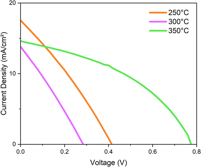 | ||
| Fig. 4 Illuminated JV curves for the devices based on CZTS NPs HTM annealed at 350 °C, 300 °C and 250 °C. | ||
Compared to SAM HTM, PSCs with CZTS NPs HTM showed poor photovoltaic performance with low Jsc and FF. This may be due to the non-uniformity of the HTM layer, composed of semiconductive NPs interconnected by an insulating polymer, ethyl cellulose. A future challenge emerging from this work could be incorporating organic conductive molecules into the CZTS NPs layer. More importantly, SEM images of the SAM and CZTS NPs films reveal significant differences in surface morphology. The AFM and SEM analyses (Fig. S6†) show that the SAM (MeO-2PACz) films offer uniform coverage at sub-μm and tens-of-μm scales. At a scale of 200 nm, regular structures associated with the molecular organisation of the MeO-2PACz are observed, with height variations substantially confined to less than 10 nm. In contrast, the CZTS films, while effectively covering the perovskite, exhibit a relatively much higher density of inhomogeneities. Namely, large agglomerates are detected, both by AFM and SEM, with lateral size and height exceeding 300 nm. The irregular structure of the CZTS film compromises the effective charge extraction since the agglomerates observed on the surface of the CZTS film could create localised points prone to short-circuiting the device. Efforts are underway to develop a novel deposition method to prevent their formation, thereby enhancing the uniformity of the CZTS NPs films.
Based on the above results, the 350-CZTS HTM was selected to investigate perovskite solar cell stability further. The performance of the CZTS-based device was compared to a control device using the common SAM HTM, as shown in Fig. 5. This figure presents the illuminated current–voltage curves of the two investigated devices, the CZTS-based and the control perovskite solar cells. Fig. 5, along with Tables 2 and 3, reveals a decline in performance for the control device, while the performance of the CZTS-based solar cell improves, indicating superior stability.
 | ||
| Fig. 5 JV curves under illuminated conditions of the CZTS-based and the control devices measured over days to investigate the stability of both the perovskite solar cells. | ||
| CZTS | J sc (mA cm−2) | V oc (V) | FF (%) | PCE (%) |
|---|---|---|---|---|
| w0 | 14.64 | 0.77 | 41.58 | 4.71 |
| w1 | 16.55 | 0.70 | 47.59 | 5.89 |
| w2 | 15.72 | 0.81 | 49.91 | 6.38 |
| w3 | 16.57 | 0.83 | 45.30 | 6.24 |
| w10 | 16.97 | 0.81 | 45.59 | 6.26 |
| w16 | 16.18 | 0.79 | 48.89 | 6.24 |
| w18 | 17.09 | 0.78 | 45.08 | 6.04 |
| SAM | J sc (mA cm−2) | V oc (V) | FF (%) | PCE (%) |
|---|---|---|---|---|
| w0 | 17.75 | 0.96 | 52.58 | 8.94 |
| w1 | 18.24 | 0.96 | 68.60 | 12.07 |
| w2 | 17.05 | 0.97 | 65.60 | 10.84 |
| w3 | 17.60 | 0.97 | 49.38 | 8.44 |
| w10 | 20.16 | 0.66 | 50.07 | 6.67 |
| w16 | 16.87 | 0.79 | 53.51 | 7.11 |
| w18 | 20.04 | 0.76 | 45.18 | 6.87 |
This trend is further confirmed by the box charts in Fig. S7 and S8,† which display the solar parameters of 64 additional devices. The enhanced stability of the CZTS-based device is also evident in the EQE spectra shown in the ESI (Fig. S9).† With time, the control device decreases the overall quantum efficiency in the region below 600 nm and above. At the short wavelength, the dominant recombination occurs near the front contact interface (HTM/MAPbI3), so EQE confirms the improvement with time of the charge extraction operated by CZTS NPs while highlighting the degradation of the SAM efficiency.12,79 EQE also justifies the overall lower efficiency of the CZTS-based device, showing that the parasitic absorption of the HTM heavily impacts the light that the device can exploit.12,79 Transmittance spectra (Fig. S10†) confirm this evaluation and highlight the reduced optical transmittance of the CZTS NPs layer compared to the MeO-2PACz one. This reduction in transmittance, particularly in the visible range, heavily impacts the light available for effective photoelectric conversion. This can be overcome by inverting the architecture to exploit the stabilising properties of CZTS NPs. Accordingly, it is increasingly urgent to design an ink that can be deposited at lower temperatures than those explored here.
A discrepancy between the Jsc derived from the EQE integration and that obtained using the solar simulator (SS) was observed, with Jsc-EQE higher than Jsc-SS. Although less common, this behaviour can be explained by considering two main factors.
First, the illuminated area during the J–V measurements (0.09 cm2) is larger than that used for the EQE measurements (0.05 cm2). Perovskites exhibit a non-uniform chemical composition and defect concentration across the film, and a larger tested area can lead to lower PV performance.80 Second, the solar simulator used is calibrated with a photodiode designed for organic cells, which partially filters the UV components of the spectrum.81 This spectral mismatch can affect the measurement of Jsc-SS compared with the EQE, which uses a calibrated monochromatic source. The observed results are, therefore, consistent with the intrinsic characteristics of perovskites and with the experimental conditions adopted.
The superior performance of the CZTS-based cell is further illustrated by the IV characteristic measured in dark conditions (Fig. S11†), where the built-in potential is absent over different days for the CZTS-based device, in contrast to the control device. The minimum of the dark curves at zero voltage for the CZTS NPs-based devices suggests that the CZTS/MAPbI3 interface is less prone to ion accumulation than that between SAM and MAPbI3.82 However, the dark current in the CZTS-based PSCs is higher than that of the conventional devices. In the former, the dark current can be due to the non-uniformity of the CZTS NPs layer or thermal charge generation at the CZTS NPs/MAPbI3 interface. Ollearo et al. demonstrated that the activation energy (Ea) of this thermal process is comparable to the energy difference φ between the CBM of the perovskite and the VBM (or HOMO level, depending if the HTM is organic or not) of the HTM.83 Therefore, they suggest that the VBM of the HTM also influences the dark current due to the thermally activated charge generation. In our case, a higher dark current for the CZTS NPs-based PSCs could suggest that the band alignment between CZTS and MAPbI3 is not ideal—however, the HOMO level for SAM MeO-2PACz reported by Ollearo et al.83 It is close to the VBM of the 350-CZTS layer reported in Fig. 3, around 5.2 eV. Thus, in the present case, the Ea may be due to oleylamine and ethyl cellulose residues affecting the interface between the CZTS NPs HTM and the MAPbI3, potentially reducing the thermal charge generation Ea at this interface.
To further assess the stability enhancement by the inorganic HTM, a reference device and a CZTS-based device were subjected to highly humid conditions (70% relative humidity at 30 °C) and periodically measured using a solar simulator. Fig. 6 presents the trends in photovoltaic parameters observed over various hours of exposure to high humidity. After 72 hours, both devices ceased to function, although the performance of the CZTS NPs HTM device was consistently better than that of the reference device. This suggests that the perovskite degradation was slower in the CZTS-based device despite a silver back contact, which typically accelerates perovskite degradation under humid conditions.
 | ||
| Fig. 6 PSCs parameters trends after various hours under moisture conditions. | ||
3.3 CZTS NPs/MAPbI3 interface
Over time, the improved stability and increased PV performance of the CZTS NPs-based PSCs suggest a different interaction between the MAPbI3 and the CZTS NPs than between the perovskite and the SAM. Steady-state photoluminescence (PL) and time-resolved photoluminescence (TRPL) analyses were conducted on fresh and aged samples to understand these interfaces better. These measurements were performed on the investigated CZTS NPs/MAPbI3 interface, the control SAM/MAPbI3 interface, and the bare MAPbI3 layer. Fig. 7 shows the normalised PL spectra for the three samples, glass/ITO/MAPbI3, glass/ITO/350-CZTS/MAPbI3 and glass/ITO/SAM/MAPbI3, and their evolution over time. The samples were stored in air atmosphere, in a box with silica gel absorbing part of the environmental moisture, to evaluate any change in PL spectra due to the deterioration of the HTM/MAPbI3 interfaces. From the spectra of day one, it is possible to see that all the peaks are centred around 770.2 nm, in line with the PL peak position of MAPbI3, 770.0 nm.84 Additionally, after days of ageing, the peak position remained consistent, suggesting the absence of phase segregation, typically evidenced by a shift in the peak position. The main difference among these spectra is the reduced emission of the MAPbI3 on the CZTS NPs layer. | ||
| Fig. 7 Steady-state PL spectra of (a) MAPbI3, SAM/MAPbI3 and CZTS/MAPbI3 compared at day 1 of ageing. PL spectra from day 1 to day 49 of ageing of (b) MAPbI3, (c) SAM/MAPbI3 and (d) CZTS/MAPbI3 samples. | ||
This result, along with the faster decay of the CZTS TRPL spectra compared to the SAM spectra, Fig. 8, suggests that the photogenerated holes are rapidly transferred from the perovskite to our HTM, reducing the number of radiatively recombining charge carriers. This results in more efficient hole extraction at the CZTS NPs/MAPbI3 interface.85Table 4 shows the trap-mediated recombination lifetime (τ1) and the radiative recombination lifetime (τ2) values of the three PL samples. The faster quenching of the PL emission in the CZTS NPs/MAPbI3 sample indicates a more effective charge transfer at this interface again. The notable behaviour observed in the CZTS-based devices is the increase in efficiency can be attributed to a different interaction between the MAPbI3 perovskite and the CZTS compared to the SAM, with the CZTS promoting a more efficient charge transfer. These results align with recent studies highlighting the effectiveness of chalcogenide materials in passivating lead-related defects (Pb2+ and Pb0), thus increasing the device stability.86
 | ||
| Fig. 8 TRPL spectra of (a) MAPbI3, SAM/MAPbI3 and CZTS/MAPbI3 compared at day 1 of ageing. PL spectra from day 1 to day 49 of ageing of (b) MAPbI3, (c) SAM/MAPbI3 and (d) CZTS/MAPbI3 samples. | ||
| τ (ns) | MAPbI3 | SAM/MAPbI3 | 350-CZTS/MAPbI3 |
|---|---|---|---|
| τ 1 | 19.33 | 17.16 | 12.67 |
| τ 2 | 65.98 | 44.93 | 30.14 |
4. Conclusions
This study successfully demonstrated the enhanced stability of inverted PSCs using CZTS NPs as an HTM. Incorporating CZTS NPs led to significantly improved device longevity compared to organic HTMs, such as MeO-2PACz. Devices with CZTS NPs showed more resilience to environmental degradation, particularly humidity, and increased PCE over time, suggesting that the CZTS NPs/MAPbI3 interface matures, enhancing charge transfer efficiency. Specifically, the optimised CZTS-based devices retained higher performance after several weeks, outperforming their organic HTM counterparts. PL and TRPL analyses showed that CZTS NPs improved hole extraction efficiency from the perovskite layer, resulting in better charge transfer and reduced recombination than organic HTMs. Although challenges remain, such as improving the uniformity and conductivity of the CZTS layer and decreasing the treatment's temperature, this research paves the way for developing more robust, sustainable, and efficient perovskite solar cells by leveraging earth-abundant materials like CZTS, making PSCs more viable for commercial applications.Data availability
The data supporting this article have been included in the ESI.†Author contributions
EF: data curation, formal analysis, funding acquisition, investigation, methodology, visualisation, writing – original draft, writing – review & editing; AHH: investigation, methodology, writing – review & editing; RP: supervision, validation, writing – review & editing; KVV: investigation, resources, validation, visualisation, writing – original draft; JMG: investigation, resources, validation, visualisation, writing – original draft; AAA: data curation, formal analysis; EP: resources, supervision; MLD: resources, supervision; TW: funding acquisition, resources, supervision; AM: data curation, formal analysis, writing – review & editing; GT: methodology, validation, writing – review & editing; AS: funding acquisition, resources, validation, supervision; VT: conceptualisation, data curation, formal analysis, funding acquisition, investigation, methodology, project administration, supervision, validation, writing – original draft, writing – review & editing; SB: funding acquisition, project administration, resources, supervision.Conflicts of interest
There are no conflicts to declare.Acknowledgements
The authors gratefully thank the VIPERLAB project funded by the European Union's Horizon 2020 research and innovation program under grant agreement No. 101006715. Thanks also to the University of Milan-Bicocca through the fund 2023-ATEQC-0078, Fondo di Ateneo Quota Competitiva. The authors also thank the MUSA (Multilayered Urban Sustainability Action) project, funded by the European Union – NextGenerationEU, under the National Recovery and Resilience Plan (NRRP) Mission 4 Component 2 Investment Line 1.5: Strengthening of research structures and creation of R&D “innovation ecosystems”, set up of “territorial leaders in R&D”. JM thanks the EPSRC Programme Grant ATIP (Application Targeted and Integrated Photovoltaics) (EP/T028513/1) and the Advanced Imaging of Materials (AIM) facility at Swansea University which was funded in part by the EPSRC (EP/M028267/1) and the European Regional Development Fund through the Welsh Government (80708).References
- W. L. Filho, T. Wall, A. L. Salvia, M. A. P. Dinis and M. Mifsud, Sci. Rep., 2023, 13, 20582 CrossRef CAS PubMed.
- N. Della Valle, G. Ulpiani and N. Vetters, Humanities and Social Sciences Communications, 2023, vol. 10, p. 440 Search PubMed.
- E. Karola Velten, C. Calipel, M. Duwe, N. Evans, C. Felthöfer, J. Gardiner, M. Hagemann, F. Hossfeld, C. Humphreys, L. Kahlen, S. Lalieu, M. Leśniak, P. Schöberlein, A. Śniegocki, A. Stefańczyk and J. Tarpey, State of EU progress to climate neutrality, European Climate Neutrality Observatory, 2024 Search PubMed.
- S. Matemilola, O. Fadeyi and T. Sijuade, in Encyclopedia of Sustainable Management, ed. S. Idowu, R. Schmidpeter, N. Capaldi, L. Zu, M. Del Baldo and R. Abreu, Springer International Publishing, Cham, 2020, ch. 516-1, pp. 1–5 Search PubMed.
- H. Ritchie and M. Roser, Our World in Data, 2024 Search PubMed.
- E. Commission, Research and Innovation for Climate Neutrality by 2050: Challenges, Opportunities and the Path Forward, Luxembourg, 2024 Search PubMed.
- I. Kougias, N. Taylor, G. Kakoulaki and A. Jäger-Waldau, Renewable Sustainable Energy Rev., 2021, 144, 111017 CrossRef CAS.
- R. Jose, T. M. Brown and J. K. Ling, Perovskite Solar Cells: Prospects of Commercialization, Elsevier Science, 2024 Search PubMed.
- L. M. Herz, ACS Energy Lett., 2017, 2, 1539–1548 CrossRef CAS.
- Y. Cheng, Y. Peng, A. K. Y. Jen and H.-L. Yip, Sol. RRL, 2021, 6, 2100545 CrossRef.
- T. Webb, S. J. Sweeney and W. Zhang, Adv. Funct. Mater., 2021, 31, 2103121 CrossRef CAS.
- V. Trifiletti, N. Manfredi, A. Listorti, D. Altamura, C. Giannini, S. Colella, G. Gigli and A. Rizzo, Adv. Mater. Interfaces, 2016, 3, 1600493 CrossRef.
- V. Trifiletti, V. Roiati, S. Colella, R. Giannuzzi, L. De Marco, A. Rizzo, M. Manca, A. Listorti and G. Gigli, ACS Appl. Mater. Interfaces, 2015, 7, 4283–4289 CrossRef CAS PubMed.
- N. G. Park, Adv. Energy Mater., 2019, 10, 1903106 CrossRef.
- M. R. Samantaray, Z. Wang, D. Hu, M. Yuan, H. Song, F. F. Li, G. Jia, L. Ji, X. Zou, H. H. Shen, B. Xi, Y. Tian, X. Q. Xu, D. J. Lee and H. Y. Hsu, Sol. RRL, 2024, 8, 2400235 CrossRef CAS.
- Z. Guo, A. K. Jena, G. M. Kim and T. Miyasaka, Energy Environ. Sci., 2022, 15, 3171–3222 RSC.
- P. Caprioglio, J. A. Smith, R. D. J. Oliver, A. Dasgupta, S. Choudhary, M. D. Farrar, A. J. Ramadan, Y. H. Lin, M. G. Christoforo, J. M. Ball, J. Diekmann, J. Thiesbrummel, K. A. Zaininger, X. Shen, M. B. Johnston, D. Neher, M. Stolterfoht and H. J. Snaith, Nat. Commun., 2023, 14, 932 CrossRef CAS PubMed.
- D. Burkitt, R. Patidar, P. Greenwood, K. Hooper, J. McGettrick, S. Dimitrov, M. Colombo, V. Stoichkov, D. Richards, D. Beynon, M. Davies and T. Watson, Sustainable Energy Fuels, 2020, 4, 3340–3351 RSC.
- X. Zhang, L. Shen, P. Baral, S. N. Vijayaraghavan, F. Yan, X. Gong and H. Wang, Sol. Energy Mater. Sol. Cells, 2022, 246, 111894 CrossRef CAS.
- Y. Ma, Z. Lu, X. Su, G. Zou and Q. Zhao, Adv. Energy Sustainability Res., 2022, 4, 2200133 CrossRef.
- P. Zhu, C. Chen, J. Dai, Y. Zhang, R. Mao, S. Chen, J. Huang and J. Zhu, Adv. Mater., 2024, 36, e2307357 CrossRef PubMed.
- Y. Ding, Q. Guo, Y. Geng, Z. Dai, Z. Wang, Z. Chen, Q. Guo, Z. Zheng, Y. Li and E. Zhou, Nano Today, 2022, 46, 101586 CrossRef CAS.
- C. Duan, A. Tang, Q. Guo, W. Zhang, L. Yang, Y. Ding, Z. Dai and E. Zhou, Adv. Funct. Mater., 2024, 34, 2313462 CrossRef CAS.
- K. Sun and P. Müller-Buschbaum, Energy Technol., 2023, 11, 2201475 CrossRef CAS.
- B. P. Kore, M. Jamshidi and J. M. Gardner, Mater. Adv., 2024, 5, 2200–2217 RSC.
- S. Baumann, G. E. Eperon, A. Virtuani, Q. Jeangros, D. B. Kern, D. Barrit, J. Schall, W. Nie, G. Oreski, M. Khenkin, C. Ulbrich, R. Peibst, J. S. Stein and M. Köntges, Energy Environ. Sci., 2024, 17, 7566–7599 RSC.
- H. Zhang, J. W. Lee, G. Nasti, R. Handy, A. Abate, M. Gratzel and N. G. Park, Nature, 2023, 617, 687–695 CrossRef CAS PubMed.
- F. Kong, E. Güzel and S. Sonmezoglu, Mater. Today Energy, 2023, 35, 101324 CrossRef CAS.
- İ. C. Kaya, R. Ozdemir, H. Usta and S. Sonmezoglu, J. Mater. Chem. A, 2022, 10, 12464–12472 RSC.
- S. Sajid, S. Alzahmi, I. B. Salem, J. Park and I. M. Obaidat, Mater. Today Energy, 2023, 37, 101378 CrossRef CAS.
- S. Akin, Y. Liu, M. I. Dar, S. M. Zakeeruddin, M. Grätzel, S. Turan and S. Sonmezoglu, J. Mater. Chem. A, 2018, 6, 20327–20337 RSC.
- S. Akin, F. Sadegh, S. Turan and S. Sonmezoglu, ACS Appl. Mater. Interfaces, 2019, 11, 45142–45149 CrossRef CAS PubMed.
- M. A. K. Sanhoury, in Handbook of Energy Materials, ed. R. Gupta, Springer Nature Singapore, Singapore, 2023, ch. 68-1, pp. 1–23 Search PubMed.
- J. J. Chaudhari and U. S. Joshi, J. Mater. Sci.: Mater. Electron., 2020, 31, 14411–14420 CrossRef CAS.
- A. Le Donne, V. Trifiletti and S. Binetti, Front. Chem., 2019, 7, 297 CrossRef CAS PubMed.
- U. A. Shah, A. Wang, M. Irfan Ullah, M. Ishaq, I. A. Shah, Y. Zeng, M. S. Abbasi, M. A. Umair, U. Farooq, G. X. Liang and K. Sun, Small, 2024, 20, e2310584 CrossRef PubMed.
- G. Tseberlidis, C. Gobbo, V. Trifiletti, V. Di Palma and S. Binetti, Sustainable Mater. Technol., 2024, 41, e01003 CrossRef CAS.
- G. Tseberlidis, V. Trifiletti, A. Le Donne, L. Frioni, M. Acciarri and S. Binetti, Sol. Energy, 2020, 208, 532–538 CrossRef CAS.
- V. Trifiletti, S. Mostoni, F. Butrichi, M. Acciarri, S. Binetti and R. Scotti, ChemistrySelect, 2019, 4, 4905–4912 CrossRef CAS.
- NREL, The National Renewable Energy Laboratory. Best Research-Cell Efficiency Chart, https://www.nrel.gov/pv/cell-efficiency.html, accessed 24/11/2024.
- B. Ananthoju, J. Mohapatra, D. Bahadur, N. V. Medhekar and M. Aslam, Sol. Energy Mater. Sol. Cells, 2019, 189, 125–132 CrossRef CAS.
- U. Syafiq, N. Ataollahi and P. Scardi, Sol. Energy, 2020, 196, 399–408 CrossRef CAS.
- Q. Wu, C. Xue, Y. Li, P. Zhou, W. Liu, J. Zhu, S. Dai, C. Zhu and S. Yang, ACS Appl. Mater. Interfaces, 2015, 7, 28466–28473 CrossRef CAS PubMed.
- A. S. Nazligul, M. Wang and K. L. Choy, Sustainability, 2020, 12, 5138 CrossRef CAS.
- P. Semalti, V. Sharma and S. N. Sharma, J. Cleaner Prod., 2022, 365, 132750 CrossRef CAS.
- L. S. Khanzada, I. Levchuk, Y. Hou, H. Azimi, A. Osvet, R. Ahmad, M. Brandl, P. Herre, M. Distaso, R. Hock, W. Peukert, M. Batentschuk and C. J. Brabec, Adv. Funct. Mater., 2016, 26, 8300–8306 CrossRef CAS.
- Y. Zuo, L. Chen, W. Jiang, B. Liu, C. Zeng, M. Li and X. Shi, Mater. Tehnol., 2018, 52, 483–486 CrossRef CAS.
- G. Y. Ashebir, C. Dong, Z. Wan, J. Qi, J. Chen, Q. Zhao, W. Chen and M. Wang, J. Phys. Chem. Solids, 2019, 129, 204–208 CrossRef CAS.
- S. B. Patel, A. H. Patel and J. V. Gohel, CrystEngComm, 2018, 20, 7677–7687 RSC.
- C. Steinhagen, M. G. Panthani, V. Akhavan, B. Goodfellow, B. Koo and B. A. Korgel, J. Am. Chem. Soc., 2009, 131, 12554–12555 CrossRef CAS PubMed.
- A. H. Husien, G. Tseberlidis, V. Trifiletti, E. Fabbretti, S. Mostoni, J. McGettrick, T. Watson, R. Po and S. Binetti, Nanoscale Adv., 2024, 7, 250–260 Search PubMed.
- G. Tseberlidis, V. Trifiletti, A. H. Husien, A. L'Altrella, S. Binetti and F. Gosetti, Appl. Sci., 2024, 14, 9923 CrossRef CAS.
- N. Vanni, R. Po, P. Biagini, G. Bravetti, S. Carallo, A. Giuri and A. Rizzo, Nanomaterials, 2024, 14, 107 CrossRef CAS PubMed.
- D. Burkitt, R. Swartwout, J. McGettrick, P. Greenwood, D. Beynon, R. Brenes, V. Bulovic and T. Watson, RSC Adv., 2019, 9, 37415–37423 RSC.
- E. V. Pean, S. Dimitrov, C. S. De Castro and M. L. Davies, Phys. Chem. Chem. Phys., 2020, 22, 28345–28358 RSC.
- P. Kush and S. Deka, Mater. Chem. Phys., 2015, 162, 608–616 CrossRef CAS.
- Y. A. Aggour, J. Mater. Sci., 2000, 35, 1623–1627 CrossRef CAS.
- Z. Xu, P. Chen, Z. Wu, F. Xu, G. Yang, B. Liu, C. Tan, L. Zhang, R. Zhang and Y. Zheng, Mater. Sci. Semicond. Process., 2014, 26, 588–592 CrossRef CAS.
- J. Wang, P. Zhang, X. Song and L. Gao, RSC Adv., 2014, 4, 27805–27810 RSC.
- S. Ahmadi, N. Khemiri, A. Cantarero and M. Kanzari, J. Alloys Compd., 2022, 925, 166520 CrossRef CAS.
- C. Mongioví, G. Crini, X. Gabrion, V. Placet, V. Blondeau-Patissier, A. Krystianiak, S. Durand, J. Beaugrand, A. Dorlando, C. Rivard, L. Gautier, A. R. L. Ribeiro, D. Lacalamita, B. Martel, J.-N. Staelens, A. Ivanovska, M. Kostić, O. Heintz, C. Bradu, M. Raschetti and N. Morin-Crini, Chem. Eng. J. Adv., 2022, 10, 100282 CrossRef.
- S.-Y. Ahn, K. Park, D. Choi, J. Park, Y. J. Kim and H.-S. Kim, Electronics, 2019, 8, 1099 CrossRef CAS.
- A. V. Naumkin, A. Kraut-Vass, S. W. Gaarenstroom and C. J. Powell, NIST X-ray Photoelectron Spectroscopy Database, https://srdata.nist.gov/xps/, accessed 29/12/2024.
- J. Chen, F. Wang, B. Yang, X. Peng, Q. Chen, J. Zou and X. Dou, Coatings, 2019, 9, 130 CrossRef.
- W. Liu, B. Guo, X. Wu, F. Zhang, C. L. Mak and K. Wong, J. Mater. Chem. A, 2013, 1, 3182–3186 RSC.
- J. Chastain and R. C. King Jr, Handbook of X-ray photoelectron spectroscopy, Perkin-Elmer Corporation, 1992, vol. 40, p. 221 Search PubMed.
- D. G. Buldu, A. Cantas, F. Turkoglu, F. G. Akca, E. Meric, M. Ozdemir, E. Tarhan, L. Ozyuzer and G. Aygun, Phys. Scr., 2018, 93, 024002 CrossRef.
- P. M. Shanthi, P. J. Hanumantha, K. Ramalinga, B. Gattu, M. K. Datta and P. N. Kumta, J. Electrochem. Soc., 2019, 166, A1827–A1835 CrossRef CAS.
- N. Hellgren, R.T. Haasch, S. Schmidt, L. Hultman and I. Petrov, Carbon, 2016, 108, 242–252 CrossRef CAS.
- S. M. Ansari, B. B. Sinha, D. Sen, P. U. Sastry, Y. D. Kolekar and C. V. Ramana, Nanomaterials, 2022, 12, 3015 CrossRef CAS PubMed.
- J. Tang, S. Li, Y. Wang, H. Zhang, B. Lin and M. Sun, Prog. Org. Coat., 2022, 163, 106617 CrossRef CAS.
- C. Tamin, D. Chaumont, O. Heintz, A. Leray and M. Adnane, EPJ Photovoltaics, 2022, 13, 24 CrossRef CAS.
- S. Pandharkar, S. Rondiya, A. Bhorde, S. Nair, R. Aher, P. Vairale, A. Waghmare, D. Naik, R. Waykar and Y. Jadhav, J. Mater. Sci.: Mater. Electron., 2019, 30, 14781–14790 CrossRef CAS.
- Y. Tan, D. Fang, N. Cheng, F. Xiong, W. Ding, B. Mi and Z. Gao, Mater. Sci. Semicond. Process., 2023, 166, 107710 CrossRef CAS.
- R. Aruna-Devi, M. Latha, S. Velumani and J. Á. Chávez-Carvayar, Rare Met., 2019, 40, 2602–2609 CrossRef.
- J. Jasieniak, M. Califano and S. E. Watkins, ACS Nano, 2011, 5, 5888–5902 CrossRef CAS PubMed.
- S. ğit Gezgin and H. Ş. Kiliç, Opt. Mater., 2020, 101, 109760 CrossRef.
- S. Yiğit Gezgin and H. Ş. Kiliç, Indian J. Phys., 2022, 97, 779–796 CrossRef.
- H. Fujiwara, M. Kato, M. Tamakoshi, T. Miyadera and M. Chikamatsu, Phys. Status Solidi A, 2018, 215, 1700730 CrossRef.
- G. Yan, Y. Yuan, M. Kaba and T. Kirchartz, Adv. Energy Mater., 2024, 2403706 Search PubMed.
- S. Ye, B. Chen, Y. Cheng, M. Feng, H. Rao, Y. M. Lam and T. C. Sum, J. Phys. Chem. Lett., 2020, 11, 3782–3788 CrossRef CAS PubMed.
- J. Y. Huang, Y. W. Yang, W. H. Hsu, E. W. Chang, M. H. Chen and Y. R. Wu, Sci. Rep., 2022, 12, 7927 CrossRef CAS PubMed.
- R. Ollearo, J. Wang, M. J. Dyson, C. H. L. Weijtens, M. Fattori, B. T. van Gorkom, A. van Breemen, S. C. J. Meskers, R. A. J. Janssen and G. H. Gelinck, Nat. Commun., 2021, 12, 7277 CrossRef CAS PubMed.
- J. I. Khan, F. H. Isikgor, E. Ugur, W. Raja, G. T. Harrison, E. Yengel, T. D. Anthopoulos, S. De Wolf and F. Laquai, ACS Energy Lett., 2021, 6, 4155–4164 CrossRef CAS.
- S. N. Habisreutinger, B. Wenger, H. J. Snaith and R. J. Nicholas, ACS Energy Lett., 2017, 2, 622–628 CrossRef CAS.
- A. Sadhu, Y. Guo, T. Salim, Q. Sun, S. G. Mhaisalkar, T. C. Sum and L. H. Wong, Adv. Funct. Mater., 2023, 33, 2305215 CrossRef CAS.
Footnote |
| † Electronic supplementary information (ESI) available: Which reports positions and identifications of the main peaks in XPS spectra for CZTS NPs film annealed at 350 °C, 300 °C and 250 °C; high-resolution XPS spectrum of Cu 2p of CZTS NPs powder, for Cu 2p, Zn 2p, Sn 3d and S 2p components of CZTS NPs film annealed at 300 °C and at 250 °C; XPS spectra of impurities containing N 1s and C 1s; UPS spectrum for CZTS NPs films annealed at 350 °C, 300 °C and 250 °C; Kubelka–Munk plot; box charts indicating the trend of devices' performances over several days. See DOI: https://doi.org/10.1039/d4se01309c |
| This journal is © The Royal Society of Chemistry 2025 |