Infrared response of multiwalled boron nitride nanotubes
E.
Borowiak-Palen
*ac,
T.
Pichler
ab,
G. G.
Fuentes
a,
B.
Bendjemil
a,
X.
Liu
a,
A.
Graff
a,
G.
Behr
a,
R. J.
Kalenczuk
c,
M.
Knupfer
a and
J.
Fink
a
aLeibniz Institute for Solid State and Material Research Dresden, D-01171, Dresden, Germany. E-mail: E.Borowiak@IFW-Dresden.de; Fax: 49 351 4659 440; Tel: 49 351 4659 501
bUniversität Wien, Institut für Materialphysik, Strudlhofgasse 4, A-1090, Wien, Austria. E-mail: pichler@ap.univie.ac.at; Fax: 43 1 4277 51357; Tel: 43 1 4277 51369
cTechnical University of Szczecin, Instutite of Chemical and Environment Engineering, Szczecin, Poland. E-mail: rk@mailbox.ps.pl; Fax: 48 91449 4730; Tel: 48 91449 4730
First published on 26th November 2002
Abstract
We report the infrared (IR) response of bulk samples of multiwalled boron nitride nanotubes, produced by a substitution reaction from single walled carbon nanotubes, which is dominated by two characteristic BN-vibrations at 800 and 1372 cm−1.
During recent years boron nitride nanotubes (BNNT) have received the attention of researchers due to their large gap semiconducting1 character and high structural stability, which render this material suitable for application in photoluminescence devices.2 The electronic and structural properties of BNNT have been theoretically investigated in detail. The dependence of the band gap of BNNT has been studied as a function of the inner diameter and the nanotube chirality,3 A strong decrease of the gap was observed for nanotube diameters below about 1.3 nm. Minimal lattice energy calculations by Hernández et al. suggest that the most favourable chirality for BNNT is zigzag.4 They also predicted a Young’s modulus of around 300 GPa for both zigzag and armchair nanotubes and some degree of buckling perpendicular to the nanotube axis. Experimentally, most of the work was performed by transmission electron microscopy (TEM)5–14 and there is much less reported on the electronic and optical properties of bulk samples of BNNT. In this communication we report the IR response of the BN vibrations in MWBNNT which can be used to characterize nanotube samples. BNNT have been first produced by arc discharge and laser ablation techniques. Most of the produced NT have zigzag geometry.
An alternative route to fabricate BNNT is the substitution of the carbon atoms of carbon nanotube templates by boron and nitrogen as reported previously by Golberg et al.11,12 and Han et al.13,14 This method is also used in our study.
For the production of our samples a 5∶2∶1 mixture in weight of laser ablation fabricated single-walled carbon nanotubes15 (SWCNT), B2O3 as a boron source and MoO3 as catalyst was heated in nitrogen atmosphere up to 1500 °C during 30 min in a high vacuum preparation chamber with a base pressure of 10−7 mbar. The resulting material was first dispersed ultrasonically in CCl4 and dropped onto KBr single crystals for the optical studies and also transferred to electron microscopy grids by subsequently dissolving the KBr in distilled water for transmission electron microscope (TEM), electron diffraction (ED) and electron energy loss (EELS) characterisation. The optical response in the IR photon energy region was measured in the absorption mode using a Bruker 113V spectrometer. The resolution was set to 0.5 cm−1. TEM, EELS and electron diffraction were performed in a Phillips CM20FEG electron microscope and in a purpose built electron energy-loss spectrometer described elsewhere,16 respectively.
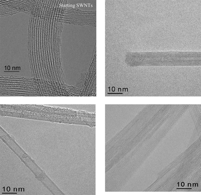
Fig. 1 shows typical high resolution TEM images of the SWCNT templates (upper left panel) and of the grown BNNT material. Clearly, the reaction product consists of multiwalled nanotubes with 2–10 walls and diameters in the range of 3 ± 1 nm. EELS measurements (not shown) revealed a 1∶1 BN-stoichiometry without contribution of carbon in the MWNT. The arrangement of the h-BN layers in MWBNNT is similarly ordered to the graphite layers in the SWCNT in good agreement with previously reported observations. As can be seen from Fig. 1 (upper right panel) the tubes in our material are capped. A statistical analysis of our TEM images reveal a MWBNNT production yield of 98% and a only very small residual amount of amorphous carbon in the bulk sample. The creation of MWBNNT from SWCNT in our samples can be explained as a double step process. First the transition from SWCNT to MWCNT occurs as has been reported previously.17 As a second step the substitution reaction of carbon atoms by boron and nitrogen takes place leading to a multishell honeycomb like structure.
 | ||
| Fig. 1 High resolution TEM micrographs of typical SWCNT templates (upper left panel) and of three multiwalled boron nitride nanotubes after reaction. | ||
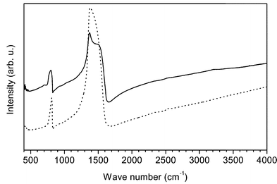
In Fig. 2 we present the measured IR response of the as grown MWBNNT (solid line) and a bulk polycrystalline h-BN reference for comparison (dotted line). The spectrum of the MWBNNT is dominated by vibrations with a strong dipole moment at 800 cm−1 (B–N vibration perpendicular to the tube axis) and at 1372 cm−1 with a pronounced shoulder at 1540 cm−1 (B–N vibration along the axis of the nanotubes). In the case of polycrystalline h-BN the corresponding modes are observed at 811 cm−1 (out-of-plane B–N vibration) at 1377 cm−1 and a weak shoulder at 1514 cm−1 (in-plane B–N vibration). We now turn to a tentative assignment of these modes. In pyrolytic h-BN two characteristic transverse optical (TO) phonon modes are observed at 767 (783) and 1367 (1510) cm−1 for the electric field polarized parallel (perpendicular) to the c-axis, respectively.18 For epitaxial monolayers of h-BN on metal surfaces which show a buckled structure with some sp3 admixture the modes are shifted to ca. 790 and 1395 cm−1.19 Both modes exhibit a strong IR response resulting in a pronounced splitting between the TO and the longitudinal optical (LO) phonon branches as observed in the IR reflectivity.18 The corresponding LO modes are observed at ca. 778 (828) cm−1 and ca. 1610 (1595) cm−1.18 For polycrystalline h-BN shown in Fig. 2 (dotted line) the observed LO–TO splitting is substantially reduced resulting in only one out-of-plane vibration at 811 cm−1 and a TO in-plane vibration at 1377 cm−1 with a weak LO in-plane component at 1514 cm−1, respectively. Since the relative spectral weight and the LO–TO splitting between the two components is related to the mixture of the oscillator strength of the modes parallel and perpendicular to the c-axes of h-BN, it can be used as a measure of the orientation of MWBNNT in the sample. In other words, a three-dimensional disorder in a polycrystalline h-BN sample results in a very small LO–TO splitting as seen in Fig. 2.
 | ||
| Fig. 2 Optical absorption spectrum of multiwalled boron nitride nanotubes (solid line) and h-boron nitride (dotted line). The peak at low frequency corresponds to a vibration between the layers (tubes), the second peak at high frequency to vibrations in the layer (in the tube). | ||
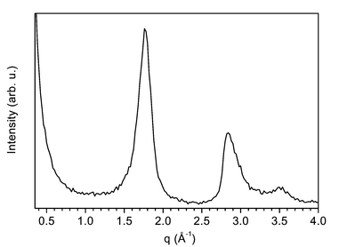
In comparison, for MWBNNT the low frequency phonon is also degenerate and shifted by about 11 cm−1 to lower wavenumber. This effect can have two possible origins. The first can be better understood by analysing the electron diffraction (ED) pattern of the grown material shown in Fig. 3. The first feature at 1.7 Å−1 of the ED pattern of MWBNNT reveals a lattice enlargement perpendicular to the BN sheets of around 6% with respect to that expected for bulk h-BN (i.e. 0.33 nm). This would lead to a reduction of the interaction perpendicular to the tube axis and consequently to a reduction of the out-of-plane phonon strength. The second interpretation arises from the modified electronic band structure of the nanotubes due to the curvature of the h-BN sheets. It is well known how the curvature of the graphene-like sheets may induce some hybridisation between π and σ states leading also to a reduction of the tight-binding overlap integral γ0. For example, SWCNT20 reveal a reduction of γ0 from 3.14 eV (i.e. graphite) down to 2.95 eV. A similar effect can be expected for the MWBNNT and can therefore be the origin of the softening of this vibration mode.
 | ||
| Fig. 3 Electron diffraction pattern of MWBNNT. | ||
The high frequency mode of the MWBNNT is, as in the case of h-BN also strongly dependent on the sample orientation and the polarisation of the light. The observed strong component at 1372 cm−1 can be assigned to the TO mode polarized along the nanotube axis. The position of the TO mode compared to h-BN is between the values for polycrystalline h-BN (1377 cm−1) and in-plane oriented pyrolytic h-BN (1367 cm−1).18 This can be explained by the fact that our nanotubes are lying on a KBr-crystal, resulting in a two-dimensional orientation of MWBNNT, and an enhancement of the IR-response and a hardening of the TO mode. The LO component, on the other hand, is much lower in intensity and therefore softened to 1540 cm−1 as compared to pyrolytic h-BN but more intense than in the polycrystalline h-BN sample (1514 cm−1) in good agreement with the explanation mentioned above.
To summarize, we have shown the IR-response of MWBNNT which can be used as a fingerprint to analyse MWBNNT in comparison with results from electron diffraction and TEM. As in h-BN for the analysis one has to be aware of the sample texture and the LO–TO splitting of the IR-active modes. Compared to polycrystalline h-BN the mode polarized perpendicular to the tube axis is softened by 11 cm−1 to 800 cm−1 and the mode polarized along the tube axis is softened by 5 cm−1 to 1372 cm−1. This is in good agreement with the observed expansion of the distance between the individual tubular shells in the electron diffraction pattern.
We acknowledge support from the EU Saturn project. The authors are grateful to K. Müller and R. Hübel for technical assistance and O. Jost for delivering the sample of SWCNT.
Notes and references
- X. Blase, A. Rubio, S. G. Louie and M. L. Cohen, Europhys. Lett., 1994, 28, 335 Search PubMed.
- X. D. Bai, E. G. Wang and J. Yu, Appl. Phys. Lett., 2000, 77, 67 CrossRef CAS.
- A. Rubio, J. L. Corkill and M. L. Cohen, Phys. Rev. B, 1994, 49, 5081 CrossRef CAS; E. Hernandez, C. Goze, P. Bernier and A. Rubio, Phys. Rev. Lett., 1998, 80, 4502 CrossRef CAS.
- E. Hernandez, C. Goze, P. Bernier and A. Rubio, Phys. Rev. Lett., 1998, 80, 4502 CrossRef CAS.
- N. G. Chopra, R. J. Luyken, K. Cherrey, V. H. Crespi, M. Cohen, S. G. Louie and A. Zettl, Science, 1995, 269, 966 CAS.
- A. Loiseau, F. Willaime, N. Demoncy, G. Hug and H. Pascard, Phys. Rev. Lett., 1996, 76, 4737 CrossRef CAS.
- M. Terrones, W. K. Hsu, H. Terrones, J. P. Zhang, S. Ramos, J. P. Hare, R. Castollo, K. Prassides, A. K. Cheetham, H. W. Kroto and D. R. M. Walton, Chem. Phys. Lett., 1996, 259, 568 CrossRef CAS.
- Y. Chen, J. Fitz Gerald, J. S. Williams and S. Bulcock, Chem. Phys. Lett., 1999, 299, 260 CrossRef CAS.
- R. S. Lee, J. Gavillet, M. Lamy de la Chapelle and A. Loiseau, Phys. Rev. B, 2001, 64, 121405 CrossRef.
- R. Ma, Y. Bando and T. Sato, Chem. Phys. Lett., 2001, 337, 61 CrossRef CAS.
- D. Golberg, Y. Bando, K. Kurashima and T. Sato, Chem. Phys. Lett., 2000, 323, 185 CrossRef CAS.
- D. Golberg, Y. Bando, L. Bourgeois, K. Kurashima and T. Sato, Carbon, 2000, 38, 2017 CrossRef CAS.
- W. Han, Y. Bando, K. Kurashima and T. Sato, Chem. Phys. Lett., 1999, 299, 368 CrossRef CAS.
- W. Han, Y. Bando, K. Kurashima and T. Sato, Appl. Phys. Lett., 1998, 73, 3085 CrossRef CAS.
- O. Jost, A. A. Gorbunov, J. Möller, W. Pompe, A. Graff, R. Friedlein, X. Liu, M. S. Golden and and J. Fink, Chem. Phys. Lett., 2001, 339, 297 CrossRef CAS.
- J. Fink, Adv. Electron. Phys., 1993, 75, 121 Search PubMed.
- K. Meteruier, S. Bonnamy, F. Beguin, C. Journet, P. Bernier, M. Lamy de la Chapelle, O. Chauvet and S. Lefrant, Carbon, 2002, 40, 1765 CrossRef.
- R. Geick, C. H. Perry and G. Rupprecht, Phys. Rev., 1966, 146, 543 Search PubMed.
- E. Rokuta, Y. Hasegawa, K. Suzuki, Y. Gamou, C. Oshima and A. Nagashima, Phys. Rev. Lett., 1997, 79, 4609 CrossRef CAS.
- X. Liu, T. Pichler, M. Knupfer, M. S. Golden, H. Kataura and and Y. Achiba, Phys. B, 2002, 66, 45411 Search PubMed.
| This journal is © The Royal Society of Chemistry 2003 |
