Titanium dioxide-based semiconductors for solar-driven environmentally friendly applications: impact of point defects on performance†
Janusz
Nowotny
*
Centre for Materials Research in Energy Conversion, School of Materials Science and Engineering, University of New South Wales, Sydney, NSW 2052, Australia. E-mail: J.Nowotny@unsw.edu.au; Fax: 61 2 9385 6467; Tel: 61 2 9385 6465
First published on 19th August 2008
Abstract
The demand for energy is rising. At the same time there is a need to increase the use of renewable energy sources in order to reduce climate change. Awareness is growing that solar energy, which is available in abundance in many countries, should be used for the production of environmentally friendly fuel and electricity. The use of solar energy is determined by availability of new materials that are able to efficiently convert solar-energy into other types of energy. It becomes increasingly clear that oxide semiconductors are the most promising candidates for solar energy conversion. These semiconductors can be used for a wide range of environmentally friendly applications, including the production of solar–hydrogen fuel and solar-driven water purification. The present work describes the concept of the use of metal oxides for the processing of high-performance photosensitive oxide semiconductors. The aim of such processing is to impose the functional properties, which are required for specific applications. The present work brings together the concepts of solid-state chemistry and the concepts of photoelectrochemistry in order to outline the research strategy of TiO2-based photosensitive oxide semiconductors.
 Janusz Nowotny | Janusz Nowotny is the Director of the Centre for Materials Research in Energy Conversion, University of New South Wales. His research is focused on materials and devices for solar energy conversion, including the generation of solar–hydrogen fuel by water photolysis and solar-driven water purification. He derived defect chemistry for several nonstoichiometric oxides and developed the theory of the reactivity for oxide semiconductors and the related charge transfer. |
1. Introduction
The price of oil has crossed US$130 a barrel and is rising. The rising cost of oil is the most visible result of shrinking fossil fuel reserves. The consumption of fossil fuels has even more dramatic impact on the economy through the increasingly apparent costs of climate change, including:• Increase of air, water and soil pollution and its impact on the environment,
• Melting polar ice, rising sea levels and reduced land area,
• Dangerous changes of ocean currents,
• More intense and more frequent extreme weather conditions leading to ecological catastrophies and increased costs for the production of food,
• Destruction of biodiversity.
Consequently, the need to reduce climate change is now considered in economic terms.
The use of renewable energy is still below the level that is required to have an impact on climate change. The reason for this limitation is mainly due to the costs of the conversion of renewable energy into usable forms of energy, such as electrical and chemical energy. The cost of photovoltaic electricity ($111 GJ−1)1 is still larger than the cost of coal-generated electricity ($5.8 GJ−1).2 Consequently, there is an urgent need to reduce the costs of the conversion of solar energy. These costs are mainly determined by the costs of solar materials available on the market at present, such as silicon.
Awareness is growing that soon a new generation of solar materials—oxide semiconductors—will be available. Their advantages include:
• The raw materials for the production of oxide semiconductors are readily available and relatively inexpensive.
• Their use is versatile as these semiconductors have a wide range of applications.
The present work considers the concept of the processing of high-performance oxide semiconductors for a wide range of environmentally friendly applications, including the production of solar–hydrogen fuel and solar-driven water purification. While titanium dioxide will be considered in the present work as an example, the general concept is valid for all nonstoichiometric oxides as well.
2. Postulation of the problem
The properties of metal oxides are frequently related to their crystallographic structures and microstructures. Awareness is growing, however, that the properties of nonstoichiometric oxides are determined even more strongly by their defect disorder rather than by their structure.3The most common procedure applied in the modification of nonstoichiometry and the related properties includes doping with cations and anions.4–6 While doping may have a substantial effect on properties and performance, the reported literature data commonly suffer from a failure to recognise the following effects:
• The effect of doping mechanism. The effect of doping depends on the location of the dopant ion in the host lattice. For example, tri-valent metal ions, such as Cr3+, introduced in Ti sites and interstitial sites of TiO2, act as acceptors and donors, respectively.
• The effect of distribution. The effect of doping depends on the location of dopants within the specimen. For example, Cr introduced into the bulk phase and the surface layer of NiO act as a donor and acceptor, respectively.7
• Effect of oxygen. Oxygen is an important dopant for metal oxides as it is a part of both the ambient atmosphere and the lattice. The effect of oxygen on properties includes both undoped specimens and solid solutions:
○ Undoped oxides. The properties of undoped (but not always pure) metal oxides are very sensitive to oxygen content in the lattice and the related nonstoichiometry. Therefore, the properties of oxides must be considered along with the specific values of oxygen nonstoichiometry. It has been shown that the properties of TiO2, and the related defect disorder, are closely related to oxygen activity.8,9 In other words, the properties reported for oxides of unknown oxygen activity are not well defined, even for single crystals with well defined crystalline structure.
○ Solid solutions. The mechanism of doping depends on oxygen activity.10 A substantial lack of compatability between the reported literature data for oxide systems is due to the lack of recognition of this effect, which is substantial.9
So far, little is known on the effect of oxygen nonstoichiometry on photocatalytic properties. Therefore, the research strategy must include the processing procedure accompanied by the imposition of controlled oxygen activity.
The effect of oxygen on the properties of oxides in the present work will be considered for titanium dioxide, TiO2, and its solid solutions, as an example. It will be shown that the chemical formula TiO2 should be considered only as a symbolic representation of a range of titanium oxides, for which the O/Ti ratio is approximately equal to 2.3 It will be shown that the semiconducting properties of TiO2, and its ability to react with water and oxygen, are strongly affected by even small changes to this ratio and the related changes of defect disorder.
The present work will consider the research strategy for the processing of well defined TiO2-based oxide semiconductors through the imposition of controlled oxygen nonstoichiometry and the related defect disorder. The present work will consider the defect chemistry of TiO2 and defect-related properties. It will be shown that the functional properties of TiO2 are closely related to defect disorder. Consequently, the search for oxide semiconductors with enhanced performance must recognise the effect of point defects (ionic and electronic) on photoelectrochemical and photocatalytic activity. Therefore, defect chemistry may be used as a framework for the processing of TiO2-based materials with controlled functional properties that are desired for specific applications. It will be shown that the properties of TiO2 may be modified in a controlled manner leading to a wide range of properties, including (i) n-type semiconducting properties with controlled chemical potential of electrons, (ii) p-type semiconducting properties, and (iii) electrical insulators. TiO2 may also be converted into a quasi-metallic conductor.11 The applications of the TiO2-based materials will be outlined, including photo-electrodes, photocatalysts, and self-cleaning coatings for building materials.
3. Nonstoichiometry of titanium dioxide
3.1. Nonstoichiometry
Photocatalytic properties of TiO2 have been frequently considered in terms of its structure (anatase and rutile).12 The first is stable at lower temperatures, while rutile, which is formed at ∼973 K (Fig. 1),13 is the thermodynamically stable structure.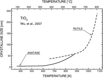 | ||
| Fig. 1 Effect of temperature on the structure (anatase vs rutile) and grain size of TiO2 according to Wu et al.13 | ||
Titanium dioxide, TiO2, is a nonstoichiometric compound, which in textbooks is represented by the formula TiO2−x, where x is the apparent oxygen nonstoichiometry.3,14 The recent studies indicate that the formula TiO2±x is more consistent with the nonstoichiometry of titanium dioxide.8,15
Awareness is growing that the properties of TiO2 are closely related to defect disorder.3,8,15 Therefore, reproducible properties may only be obtained for specimens of well defined defect disorder. So far, however, most studies have been reported for TiO2 specimens that are not well defined.
The aim of the present work is to outline the basic concept of defect chemistry for TiO2 and its use as a framework for the modification of functional properties in a controlled manner. It will be shown that any TiO2 specimen may be used as a “raw material” for the processing of TiO2-based materials with controlled properties that are desired for specific applications. The present work also considers the research strategies in the investigation of the effect of processing procedures at elevated temperatures on the functional properties at room temperature.
3.2. Defect disorder
Intrinsic point defects in TiO2 include oxygen vacancies and titanium interstitials.3,8 Recent studies have verified the formation of another defect in the Ti sublattice: titanium vacancies.16 The incorporation of extrinsic defects (aliovalent ions) into the TiO2 lattice leads to the formation of donors and acceptors when their valency is higher and lower than that of host lattice ions.The Kroeger–Vink notation of defects which reflects the charge of defects relative to the lattice,17 has been commonly used to describe defect reactions, including the reactions between defects and their formation. This notation is outlined in Table 1. The formation of intrinsic defects in TiO2 may be described by the following defect equilibria:8
 | (1) |
 | (2) |
 | (3) |
 | (4) |
 | (5) |
| No. | Species | Symbol (Kroeger–Vink notation) | Index |
|---|---|---|---|
a Full chemical formula for undoped TiO2: 
|
|||
| 1 | Titanium ion in its lattice site | TixTi | a |
| 2 | Singly ionised titanium ion in its lattice site (equivalent to quasi-free electron) | Ti′Ti | b |
| 3 | Tetra-valent titanium vacancy | V′′′′Ti | c |
| 4 | Tetra-valent titanium ion in the interstitial site | Ti˙˙˙˙i | d |
| 5 | Tri-valent titanium ion in the interstitial site | Ti˙˙˙i | e |
| 6 | Oxygen ion in its lattice site | Oxo | f |
| 7 | Mono-valent oxygen ion in its lattice site (equivalent to quasi-free electron hole) | O˙o | g |
| 8 | Doubly ionised oxygen vacancy | V˙˙o | h |
The concentration of defects must satisfy the lattice charge neutrality condition:
 | (6) |
3.3. Full chemical formula
The full (real) chemical formula of TiO2, reflecting all lattice elements that impact on properties, should include all ionic and electronic species. The following species must be taken into account for pure TiO2:8,9,15,18• Tetra-valent Ti ions in the cation lattice sites, TixTi
• Tri-valent Ti ions in their lattice sites (equivalent to quasi-free electrons), Ti′Ti
• Tetra-valent Ti vacancies, V′′′′Ti
• Tetra-valent Ti ions in interstitial sites, Ti˙˙˙˙i
• Tri-valent Ti ions in interstitial sites, Ti˙˙˙i
• Doubly ionized oxygen ions in the oxygen lattice sites, Oxo
• Singly ionised oxygen ions in its lattice sites (equivalent to quasi-electron holes), O˙o
• Doubly ionised oxygen vacancies, V˙˙o
Consequently, the real chemical formula for pure TiO2 may be expressed as:
 | (7) |
The apparent deviation from stoichiometry is a complex function of the concentrations of lattice species, which are interdependent. However, each defect combination must satisfy the following conditions:
• The conservation of the lattice site ratio. The law of the conservation of lattice site ratio requires that the sum of the concentrations of all species in the Ti and oxygen sublattices (in the molar ratio) are equal to unity and 2, respectively:
| a + b + c = 1 | (8) |
| f + g + h = 2 | (9) |
• The charge neutrality condition. The lattice charge neutrality condition requires that the lattice is always electrically neutral. Therefore:
| b + 4c = 4d + 3e + g + 2h | (10) |
The defects indexed by a and f are not involved in the condition (10) since they are electrically neutral with respect to the lattice.
The formula of TiO2 solid solutions may be derived in a similar manner by taking into account the presence of aliovalent ions in various lattice positions.
Quantitative relationship between the concentrations of both ionic and electronic defects, which are formed according to the reactions represented by expressions (1)–(5), may be obtained by the combination of the related equilibrium constants and the charge neutrality condition (10). Since the concentration of the defects is closely related to oxygen activity, the general relationship may be represented in the form of the concentration of electronic charge carriers as a function of p(O2):
 | (11) |
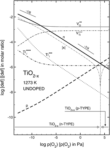 | ||
| Fig. 2 Effect of oxygen activity on isothermal concentration of ionic and electronic defects for undoped TiO2 at 1273 K. | ||
As seen, the desired properties of undoped TiO2, including n- and p-type properties as well as mixed conduction, may be achieved by the imposing controlled oxygen activity in the lattice. As also seen, the absolute value of the deviation from stoichiometry, x, assumes a minimum at the n–p transition and increases at larger p(O2). In the latter case TiO2 is a p-type semiconductor and its chemical formula is TiO2 + x.
As shown above, the physical meaning of the apparent nonstoichiometry, x, represented by the general formula TiO2 ± x is expressed by the following function of the defect-related indexes, which contribute to x:
 | (12) |
Consequently, the nonstoichiometry of TiO2 may be considered within the following cases:
 | (13) |
 | (14) |
It is essential to note, however, that the defect disorder derived by the expressions (1)–(14) corresponds to the assumptions that the predominant defects, including oxygen and Ti vacancies, are fully ionised and that Ti interstitials are mainly tri- and tetra-valent defects. The related energy levels are shown in Fig. 3.19–22
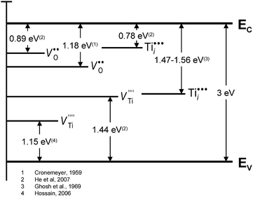 | ||
| Fig. 3 Energy levels of defects for TiO2.19–22 | ||
The ionisation degree of defects depends on temperature. Fig. 4 shows the ionisation energy of Ti vacancies of different valency.22 The picture is much more complex for TiO2 solid solutions, involving aliovalent ions, resulting in the formation of donors and acceptors of different valency. Then the full formula should be considered in terms of the location of both cations and anions in specific lattice sites and their valencies.
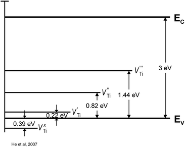 | ||
| Fig. 4 Energy levels of Ti vacancies of different ionisation degree for TiO2.22 | ||
While it has been generally assumed that at elevated temperatures the defects are fully ionised, there is a need to determine the effect of temperature on the ionisation degree.
In summary, it is essential to realise that the properties of commercial TiO2 specimens may vary within a wide range depending on the oxygen content (usually not well defined) and the concentration of impurities (sometimes provided). These properties are reflected by the extended formula for pure titanium dioxide, represented by expression (7), rather than TiO2 or TiO2 ± x. The latter formula may be considered as a general (trade) symbol of a range of titanium oxides, for which the O/Ti ratio is close to 2, and which—depending on defect disorder—may have a wide range of applications, including solar–hydrogen generation, photocatalytic water purification, gas sensing, antipollution coatings and the generation of photovoltaic electricity. Therefore, pure TiO2, with well defined defect disorder and the related properties, may be represented either by the formula (7) or in the following general form:
 | (15) |
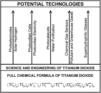 | ||
| Fig. 5 Schematic representation of the full chemical formula for undoped TiO2 and the potential applications of TiO2 with controlled defect disorder. | ||
4. Research strategy
The commonly applied research strategy to process TiO2 with desired functional properties is based on the modification of its chemical composition either by the imposition of controlled oxygen activity for pure TiO2 or by the so called doping procedure, which must be accompanied by a controlled oxygen activity. Such a procedure, which usually requires elevated temperatures, should be performed in the gas phase of a well defined oxygen activity. Intentionally, doping aims at the incorporation of aliovalent ions into the lattice. Moreover, the assessment of the effect of the applied doping procedure on performance requires several experimental cycles, including: (i) doping at elevated temperatures, (ii) subsequent cooling to room temperature, and (iii) testing the system at room temperature for the performance related quantities, such as the energy conversion efficiency, ECE. Therefore, modification of the experimental procedure requires to follow all of these cycles, which is time consuming. Therefore, in this approach, which may be considered as a trial-and-error approach, there is a substantial time gap between the processing and testing for performance. In consequence, this approach allows for the modification of the processing conditions, such as time of annealing and gas phase composition, only after several cycles, when the processing, cooling and testing, are completed. This, consequently, has an impact on the following:• The production efficiency of empirical data on the effect of processing conditions on properties.
• Incompatibility of data, which are commonly not well defined for the following reasons:
○ The processing usually takes place in a poorly defined gas phase in terms of its oxygen activity.
○ The applied cooling procedures are not well defined.
In addition, doping leads to well defined specimens only when the doping conditions of the doping process (time and temperature) are based on diffusion data for the ions used as dopants. While the diffusion data have no effect on functional properties, knowledge of these data is required to predict the processing conditions. In conclusion, the disadvantage of the trial-and-error approach includes (i) a long and complex experimental cycle required to generate empirical data, and (ii) lack of compatibility of the obtained data, which in many instances have been claimed to correspond to the same systems.
Another approach for the processing of specimens, is based on in situ monitoring of defect-related properties. This approach is based on the established relationship between the key functional properties of oxide semiconductors and their defect disorder.9 Therefore, defect chemistry may be applied as a framework for the processing of well defined oxide semiconductors with controlled properties by using in situ monitoring of both bulk and surface electrical properties during the processing at elevated temperatures and during cooling.9
The in situ monitoring approach allows:
• The imposition of controlled/enhanced properties to be achieved with a minimal delay between the time of processing and the final performance test.
• Inspection of the properties during the processing at elevated temperatures and during cooling. This allows intervention in the process while the specimen is still in the reaction chamber at elevated temperatures, including the following operations:
○ Change of the gas composition during the process,
○ Termination of the process when the specimen exhibits optimal properties. Consequently, the in situ monitoring allows for a substantial reduction of the time required for the generation of data.
The strategy of research, including the in situ monitoring approach based on defect chemistry and the trial-and-error approach, is shown in Fig. 6. As seen, the inspection may be achieved through in situ monitoring of defect-sensitive properties, including:
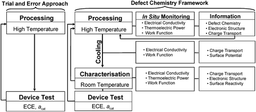 | ||
| Fig. 6 The research strategy including the trial-and-error approach, including the processing at elevated temperatures and testing at room temperature, and the “in situ” monitoring approach, which is based on continuous inspection of functional properties during processing at elevated temperatures and during cooling. | ||
• Electrical conductivity. This property allows to assess the following:
○ The electrical conductivity data are reflective of the charge transport.8
○ The electrical conductivity vs oxygen activity determined in equilibrium may be used to assess defect disorder in the bulk phase.3
○ The electrical conductivity vs temperature may be used for an assessment of electronic structure.3
○ The measurement of the electrical conductivity vs time allows the determination of the re-equilibration kinetics and the related diffusion data in the bulk.3
• Thermoelectric power. This property allows the determination of the conductivity type (carrier type/sign) and the concentration of electronic charge carriers.23 The effect of oxygen activity on thermoelectric power may be used to derive defect disorder in the bulk phase.
• Work function. As work function is directly related to the Fermi energy level at the surface, its changes may be used to assess defect disorder for the outermost surface layer. Work function may also be used for in situ determination of reactivity and the related charge transfer.24 The measurement of work function vs time allows the determination of the re-equilibration and the related diffusion data for the surface layer.
The following section will consider the effect of defect disorder on functional properties of TiO2-based oxide semiconductors, including photoelectrochemical water splitting and photocatalytic water purification.
4. Photoelectrochemical generation of solar–hydrogen
There is a general expectation that solar energy may soon be used for the generation of hydrogen fuel (solar–hydrogen).25 The most promising route for its generation is from a renewable material (water) and by using renewable energy (solar energy).26–30Since the discovery of photoelectrochemical water splitting, showing that TiO2 may be used as photo-electrode for water photolysis,26 there have been efforts aiming at the modification of TiO2 properties in order to enhance its performance.26–34 So far, however, the research has failed to increase the ECE above the level of 1–2%.33
A typical photoelectrochemical cell (PEC) for the generation of hydrogen (solar–hydrogen) involves photo-anode made of TiO2 and cathode made of Pt as is shown in Fig. 7. The basic photoelectrochemical reaction, that takes place on the surface of TiO2-based photo-anode, is the decomposition of water leading to the formation of gaseous oxygen (removed to the gas phase), hydrogen ions (transported via the aqueous electrolyte to cathode) and electrons (transported via the external circuit towards the cathode), leading to the formation of hydrogen gas at the cathode. The related charge transport within the PEC is shown in Fig. 8. The ECE for the PEC has been generally considered in term of collective properties of the photo-electrode, such as electronic structure (effect on light absorption), charge transport (effect on performance efficiency), and concentration gradients and the related electric fields (impact on the recombination-related energy losses).33
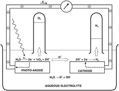 | ||
| Fig. 7 Representation of photoelectrochemical water splitting concept. | ||
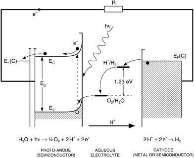 | ||
| Fig. 8 The charge transfer within the PEC formed of a semiconducting (n-type) anode and metal cathode. | ||
The performance of a PEC is strongly affected by local surface properties. It was shown that the effective charge transfer between TiO2 and water requires the presence of surface active sites that are able to provide electron holes to the adsorbed water molecules. Ti vacancies were identified as the surface active sites for water adsorption leading to the formation of an active complex and resulting, in consequence, to enhanced water splitting.34
Dye sensitization has also been used to increase the ECE of PEC.35 This type of sensitization leads to a stable performance only when the dye is resistant to corrosion and photocorrosion.
5. Photocatalytic water purification
There is a close analogy between the photocatalysts formed of TiO2 with deposited Pt islets, forming a micro-sized cell contained in a single grain, and the PECs for water splitting, which is shown in Fig. 7. The performance of a TiO2-based photocatalyst is shown in Fig. 9.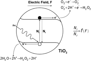 | ||
| Fig. 9 Schematic representation of photocatalytic reactivity of TiO2 and the related charge transfer, where Ni and Nr denotes the concentration of excited and recombined electrons. | ||
The function of the anodic sites may be considered in terms of the reaction between the excess of the light-induced holes and water molecules leading to the formation of hydrogen peroxide and hydrogen ions:9,35,36
 | (16) |
The most important reactive agent for the cathode is oxygen. The reactivity of the cathode may be considered in terms of the reduction of oxygen, leading to the formation of singly ionised molecular oxygen species, which subsequently react with hydrogen ions. This process has been commonly considered as the most important primary reaction step leading to the removal of electrons from the surface of photocatalysts and resulting in the formation of hydrogen peroxide:
 | (17) |
 | (18) |
The H2O2 species then react with organic molecules leading ultimately to their oxidation and the formation of harmless compounds.
An efficient photocatalytic process requires that both cathodic and anodic reactions take place with the same rate leading to efficient removal of the excess of both charge carriers at both anodic and cathodic sites. For n-type semiconductors, such as TiO2, the light-induced photo-oxidation potential, which is related to holes, is much stronger than the reduction potential.37 Therefore, in order to avoid an accumulation of less reactive electrons at the cathode, and to prevent the energy losses due to polarization and recombination, electrons must be effectively scavenged from the cathode. This may be achieved by:
• Imposition of Pt islets (or other noble metals) forming active cathodic sites,
• Imposition of a chemically induced electric field (F), which may be imposed by segregation- or diffusion-induced concentration gradients. This field leads to reduction of recombination (the recombination factor is defined by the ratio of ionised species, Ni, to recombined species, Nr). A schematic representation of photocatalytic performance for TiO2, and the related charge transfer, is shown in Fig. 9.
There has been an accumulation of reports indicating that TiO2 is a promising candidate for photocatalysts, which may be used for the removal of organic contaminants, including bacteria and viruses.35,36,38–46 The processing of TiO2 photocatalysts loaded with Pt (or other noble metals) has been focused on controlling the dispersion of Pt on the TiO2 grains.38–44 Despite that in most cases Pt results in enhanced performance, which is consistent with basic theoretical models, the performance level is below the requirements for commercial purposes. Moreover, corrosion results in deterioration of the performance of Pt-loaded photocatalysts.45,46 Therefore, Pt is not a promising candidate for the formation of cathodic sites in commercial photocatalysts. The formation of electrochemical oxide couples may be considered as an alternative to the Pt loading.
6. Alternative applications of TiO2-based oxide semiconductors
The oxidation power of TiO2 has been used to form antiseptic coatings for ceramic materials and self-cleaning coatings for building materials.47 Alternative applications include: anti-fogging coatings of mirrors, anti-pollution pavings47 and cancer treatments.48 An important application reported for dye-sensitized TiO2 also includes the generation of photovoltaic electricity.49 TiO2 has also been widely used for chemical sensing of gases, such as CO, H2, H2O, NOx, and H2S.50–587. Conclusions
Defect chemistry may be used as a framework for the processing TiO2-based materials with controlled functional properties that are desired for specific applications. It is shown that commercially available TiO2 may be used for the imposition of a wide range of properties through the imposition of controlled defect disorder, including insulating properties, n- and p-type properties, and metallic-type properties. It is shown that in situ monitoring of defect-related properties may be used for inspection of the formation process and the imposition of desired functional properties.Acknowledgements
I would like to thank to Dr Tad Bak and Dr Leigh Sheppard for their constructive comments. The present work was supported in part by the Australian Research Council and several industrial partners, including Mailmasters Pty Ltd, Brickworks Ltd, Avtronics (Australia) Ltd Pty, and Sialon Ceramics Pty Ltd. This support is sincerely appreciated.References
- Solarbuzz Cosultancy Reports, http://www.solarbuzz.com/SolarPrices.htm (14/05/08).
- F. D , Doty, http://www.dotynmr.com/PDF/Doty_H2Price.pdf (14/05/08).
- P. Kofstad, Nonstoichiometry, Diffusion and Electrical Conductivity of Binary Metal Oxides, Wiley, New York, 1972 Search PubMed.
- K. E. Karakitsou and X. E. Verykios, J. Phys. Chem., 1993, 97, 1184 CrossRef CAS.
- M. A. Malati and K. W. Wong,, Surf. Technol., 1984, 22, 305 CrossRef CAS.
- N. Serpone, D. Lawless, J. Disdier and J.-M. Herrmann, Langmuir, 1994, 10, 643 CrossRef CAS.
- J. Nowotny and M. Rekas, Solid State Ionics, 1984, 12, 253 CrossRef CAS.
- M. K. Nowotny, T. Bak and J. Nowotny, J. Phys. Chem. B, 2006, 110, 16270 CrossRef CAS.
- M. K. Nowotny, L. R. Sheppard, T. Bak and J. Nowotny, J. Phys. Chem. C, 2008, 112, 5275 CrossRef CAS.
- J.-F. Baumard and E. Tani, Phys. Status Solidi, 1977, 39, 373 Search PubMed.
- L. R. Sheppard, J. Nowotny and T. Bak, Phys. Status Solidi A, 2006, 203, R85 CrossRef CAS.
- A. G. Agros and P. Pichat, J. Photochem. Photobiol., A, 2006, 180, 130 CrossRef.
- Q. Wu, D. Li, Y. Hou, L. Wu, X. Fu and X. Wang, Mater. Chem. Phys., 2007, 102, 53 CrossRef CAS.
- Hj. Matzke, in: Nonstoichiometric Oxides, ed. O. T. Sorensen, Academic Press, New York, 1981, p. 155 Search PubMed.
- T. Bak, J. Nowotny and M. K. Nowotny, J. Phys. Chem. B, 2006, 110, 21560 CrossRef CAS.
- M. K. Nowotny, T. Bak and J. Nowotny, J. Phys. Chem. B, 2006, 110, 16302 CrossRef CAS.
- F. A. Kroger, The Chemistry of Imperfect Crystals, North Holland, Amsterdam, 1974, vol. 3, p. 275 Search PubMed.
- M. K. Nowotny, L. R. Sheppard, T. Bak and J. Nowotny, J. Phys. Chem. C, 2008, 112, 5275 CrossRef CAS.
- D. C. Cronemeyer, Phys. Rev., 1959, 113, 1222 CrossRef CAS.
- A. K. Ghosh, F. G. Wakim and R. R. Addiss, Jr, Phys. Rev., 1969, 184, 979 CrossRef CAS.
- F. M. Hossain, G. E. Murch, L. R. Sheppard and J. Nowotny, Adv. Appl. Ceram., 2007, 106, 95 Search PubMed.
- J. He, R. K. Behera, M. W. Finnis, X. Li, E. C. Dickey, S. R. Phillpot and S. B. Sinnott, Acta Mater., 2007, 55, 4325 CrossRef CAS.
- M. K. Nowotny, T. Bak and J. Nowotny, J. Phys. Chem. B, 2006, 110, 16283 CrossRef CAS.
- J. Nowotny, T. Bak, L. R. Sheppard and M. K. Nowotny, J. Am. Chem. Soc., 2008, 130, 9984 CrossRef CAS.
- O'M. Bockris, T. N. Veziroglu, D. Smith, in: Solar Hydrogen Energy, The Guernsay Press Co. Ltd., London, 1991 Search PubMed.
- A. Fujishima and K. Honda, Nature, 1972, 238, 37 CAS.
- A. Fujishima, K. Kohayakawa and K. Honda, J. Electrochem. Soc., 1975, 122, 1487 CAS.
- J. F. Houlihan, D. B. Armitage, T. Hoovler, D. Bbonaquist, D. P. Madacsi and L. N. Mulay, Mater. Res. Bull., 1978, 13, 1205 CrossRef CAS.
- C. Stalder and J. Augustinski, J. Electrochem. Soc., 1979, 126, 2007 CAS.
- H. P. Maruska and A. K. Ghosh, Sol. Energy Mater., 1979, 1, 237 CrossRef CAS.
- K. Wilke and H. D. Brauer, J. Photochem. Photobiol., A, 1999, 121, 49 CrossRef CAS.
- S. U. M. Khan, M. Al-Shahry and W. B. Ingler, Science, 2002, 297, 2243 CrossRef CAS.
- J. Nowotny, L. R. Sheppard, T. Bak and M. K. Nowotny, Int. J. Hydrogen Energy, 2007, 32, 2609 CrossRef CAS.
- J. Nowotny, T. Bak, M. K. Nowotny and L. R. Sheppard, J. Phys. Chem. B, 2006, 110, 18492 CrossRef CAS.
- O. Carp, C. L. Huisman and A. Reller, Prog. Solid State Chem., 2004, 32, 33 CrossRef CAS.
- M. R. Hoffman, S. T. Martin, W. Choi and D. W. Bahnemann, Chem. Rev., 1995, 95, 69 CrossRef CAS.
- H. Gerischer and A. Heller, J. Phys. Chem., 1991, 95, 5261 CrossRef CAS.
- M. R. St John, A. J. Furgala and A. F. Sammelle, J. Phys. Chem., 1983, 87, 801 CrossRef CAS.
- G. R. Bamwenda, S. Tsubota, T. Nakamura and M. Haruta, J. Photochem. Photobiol., A, 1995, 89, 177 CrossRef CAS.
- S. Kim and W. Choi, J. Phys. Chem. B, 2002, 106, 13311 CrossRef CAS.
- F. B. Li and X. Z. Li, Chemosphere, 2002, 48, 1103 CrossRef CAS.
- M. Anpo and M. Takeuchi, J. Catal., 2003, 216, 505 CrossRef CAS.
- S. Sakthivel, M. V. Shankar, M. Palanichamy, B. Arabindoo, D. W. Banemann and V. Murugesan, Water Res., 2004, 38, 3001 CrossRef CAS.
- S. Jin and F. Shiraishi, Chem. Eng. J., 2004, 97, 203 CrossRef CAS.
- G. R. Bamwenda, S. Tsubota, T. Nakamura and M. Haruta, J. Photochem. Photobiol., A, 1995, 89, 177 CrossRef CAS.
- V. Subramanian, E. E. Wolf and P. V. Kamat, J. Am. Chem. Soc., 2004, 126, 4943 CrossRef CAS.
- L. Wang, Sci. Am., Feb 2002, 20 Search PubMed.
- A. Fujishima, K. Hashimoto, T. Watanabe, TiO2 Photocatalysis. Fundamentals and Applications, BKC, Inc., Tokyo, 1999, pp. 14–176 Search PubMed.
- M. Gratzel, J. Sol-Gel Sci. Technol., 1994, 2, 673 CrossRef.
- R. K. Sharma, M. C. Bhatnagar and G. L. Sharma, Sens. Actuators, B, 1997, 45, 209 CrossRef.
- M. Li and Y. Chen, Sens. Actuators, B, 1992, 15, 48.
- R. K. Sharma, M. C. Bhatnager and G. I. Sharma, Sens. Actuators, B, 1988, 46, 194 Search PubMed.
- S. Akbar and L. B. Yoankman, J. Electrochem. Soc., 1997, 144, 1750.
- L. C. Birkefeld, A. M. Azad and S. Akbar, J. Am. Ceram. Soc., 1992, 75, 2694.
- G. C. Mather, F. M. B. Marques and J. R. Frade, J. Eur. Ceram. Soc., 1999, 19, 887 CrossRef CAS.
- G. Munuera, A. R. Gonalez-Elipe, A. Munoz, A. Fernandez, J. Soria, J. Conesa and J. Sanz, Sens. Actuators, 1989, 18, 337 CrossRef CAS.
- L. A. Harris, J. Electrochem. Soc., 1980, 127, 2657 CrossRef CAS.
- E. M. Logothetis and W. J. Kaiser, Sens. Actuators, 1983, 4, 333 CrossRef CAS.
Footnote |
| † Present address: Solar Energy Technologies, University of Western Sydney, Locked Bag 1797, Penrith South DC, NSW 1797, Australia; E-mail: mailto:J.Nowotny@uws.edu.au |
| This journal is © The Royal Society of Chemistry 2008 |
