Influence of alkyl substituents and thermal annealing on the film morphology and performance of solution processed, diketopyrrolopyrrole-based bulk heterojunction solar cells
Arnold
Tamayo
a,
Tyler
Kent
a,
Mananya
Tantitiwat
b,
Mark A.
Dante
a,
James
Rogers
c and
Thuc-Quyen
Nguyen
*a
aDepartment of Chemistry and Biochemistry, University of California – Santa Barbara, Santa Barbara, CA, USA. E-mail: quyen@chem.ucsb.edu
bDepartment of Physics, University of California – Santa Barbara, Santa Barbara, CA, USA
cDepartment of Materials Science and Engineering, University of California – Santa Barbara, Santa Barbara, CA, USA
First published on 14th August 2009
Abstract
A solution processable diketopyrrolopyrrole-containing oligothiophene was blended with a series of methanofullerene acceptors having different alkyl substitutents—[6,6]-phenyl C61 butyric acid methyl (PC6161BM) ester, [6,6]-phenyl C61 butyric acid hexyl ester (PC6161BH) and [6,6]-phenyl C61 butyric acid dodecyl ester (PC6161BD) to study the effect of donor–acceptor interactions on the blend film morphology and device characteristics of small molecule-based bulk heterojunction (BHJ) solar cells. A combination of characterization techniques including X-ray diffraction, atomic force microscopy, conducting atomic force microscopy, and transmission electron microscopy was used to investigate the film morphology and phase separation. The results show that changing the length of the alkyl substituent on the methanofullerene acceptor is a good approach to control the film morphology of blended films and these lead to significant differences on the performance of the as cast and annealed devices. Power conversion efficiencies between 2–3% can be reached by simple variation of the alkyl chain length.
Broader contextOrganic-based solar cells have the potential of offering a low cost, flexible, light-weight, clean, and quiet alternative energy sources for a variety of applications. The highest efficiency organic solar cell design is the bulk heterojunction (BHJ) architecture (∼5.6%) in which the active layer consists of a blend of electron donating (p-type) and electron accepting (n-type) materials forming an interpenetrating network of the hole and electron accepting components. The interpenetrating network formation depends strongly on the interactions between the donor and the acceptor and processing conditions. Here, we explore the effect of donor–acceptor interactions on the blended film morphology, phase separation, and device characteristics of solution processed diketopyrrolopyrrole-based BHJ solar cells. We found that unlike conjugated polymers, the degree of phase separation before and after thermal annealing of the blends can be controlled by the alkyl substituents on the fullerene acceptor. Changes in film morphology and phase separation lead to significant differences on the performance of the as cast and annealed devices. |
Introduction
Research interest in organic solar cells has increased significantly in recent years due to their potential as a new low-cost, flexible, sustainable and portable power source.1–3 The most efficient organic solar cells which can be entirely processed from solution are based on intimate blends of electron- and hole-transporting materials so called bulk heterojunction (BHJ) structure. Blends of polymeric p-type semiconductors and n-type methanofullerene derivatives have yielded BHJ solar cells with power conversion efficiencies that range from 4%–6%.4–6 More recently, BHJ solar cells using small molecule semiconductors have also been studied but with limited success.7–10 As cast films of p-type and n-type small molecules tend to have high surface roughness and large macroscale phase separation or crystallization, yielding lower power conversion efficiencies (PCEs).11,12 Despite this issue, small molecules are still promising materials for BHJ solar cells due to other advantages over polymers. Small molecules are monodisperse and easy to synthesize and purify. Also, BHJ solar cells using small molecules do not suffer from materials batch to batch variations associated with most polymeric donors.13,14 Furthermore, small molecules tend to have better charge transport properties than polymeric semiconductors because they are more prone to long range order.15–17In order to achieve high device efficiencies in BHJ solar cells using solution processable molecular semiconductors, it is crucial to control the film formation process to yield a continuous interpenetrating network of donor and acceptor domains for holes and electrons to travel. One way to achieve a continuous interpenetrating network in polymer-based BHJ solar cells is by varying the nature of the alkyl or solubilizing substituents attached to either donor or acceptor molecules.18–21 Choosing the optimal substituents leads to better solubility and good miscibility of the components in the film when there is a strong donor–acceptor interaction. Poor choice of substituents, on the other hand, can lead to poor solubility and large scale phase separation.22 Substituents in both components are also important when it comes to the thermal stability of blended films. Exposure of blended films to high temperatures (thermal annealing) usually give rise to various degrees of phase separation which has been found to be beneficial in blended systems such as poly(3-hexylthiophene) with [6,6]-phenyl C61 butyric acid methyl ester (P3HT : PC6161BM)23–25 but not for other donor–acceptor systems.26
Recently, we demonstrated that solution processed, small molecule-based BHJ solar cells from the blend of an oligothiophene with a diketopyrrolopyrrole core—2,5-di-(2-ethylhexyl)-3,6-bis-(5″-n-hexyl-[2,2′;5′,2″]terthiophen-5-yl)-pyrrolo[3,4-c]pyrrole-1,4-dione (SMDPPEH) and [6,6]-phenyl C61 butyric acid methyl ester (PC6161BM) can have PCEs of up to 3% under AM1.5 irradiation by manipulating the solid-state morphology (nanostructures) as a function of the donor–acceptor ratio.27,28 Aiming to understand further pure and blended film morphology formation and how this affects device performance in small molecule-based BHJ solar cells as a function of donor–acceptor interactions, we fabricated solar cell devices using commercially available methanofullerene derivatives having alkyl substituents with different lengths—PC6161BM, [6,6]-phenyl C61 butyric acid hexyl ester (PC6161BH), and [6,6]-phenyl C61 butyric acid dodecyl ester (PC6161BD) as acceptors and with SMDPPEH as the donor material (see Fig. 1). Besides having similar absorption properties and frontier energy levels, the methanofullerene derivatives studied here were specifically chosen to tune the degree of polarity of the acceptor, thus affecting the degree of molecular packing (crystallization) of the donor material. These methanofullerene derivatives have been used previously in polymer-based BHJ solar cells studies.19–21 In those studies, the alkyl chain length affects the device performance of either as cast or annealed devices but there is no clear trend between donor–acceptor interactions and the device performance. We show here that, unlike the conjugated polymer-based blended films, the absorption, crystallinity and film morphology as well as the solar cell device characteristics of both as cast and annealed blended films of diketopyrrolopyrrole (DPP)-based donors and fullerene acceptors are significantly affected by the length of the alkyl substituent attached to the methanofullerene.
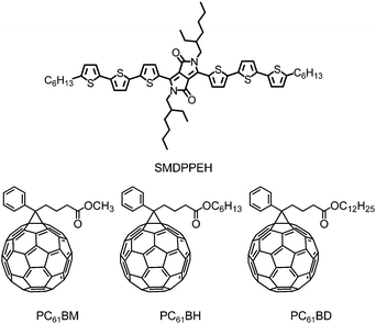 | ||
| Fig. 1 Chemical structures of SMDPPEH, PC6161BM, PC6161BH and PC6161BD. | ||
Experimental
The donor material SMDPPEH was synthesized following a reported procedure.28PC6161BM, PC6161BH, and PC6161BD were purchased from Nano-C and used as received. Anhydrous chloroform was purchased from Sigma-Aldrich company and used as received.Blended films of the methanofullerene acceptors and SMDPPEH were spun cast at 2500 rpm for 30 seconds from chloroform solutions (20 mg mL−1) onto a 40 nm layer of poly(3,4-ethylenedioxythiophene) : polystyrene sulfonate 4083, PEDOT : PSS (H.C. Starck), atop of an indium tin oxide (ITO)-coated glass (Thin Film Devices). Substrates were cleaned before use by ultrasonic treatment in isopropyl alcohol followed UV/ozone treatment (UVO Cleaner 42, Jelight Co., Inc.) for one hour prior to film deposition. The active layer thicknesses in all devices were approximately 80 nm as measured using a profilometer (Ambios XP-100).
UV-Vis absorption of pure and blended films were recorded using a Shimadzu UV-2401 PC diode array spectrometer. Thermal analysis of a pure sample of SMDPPEH was performed using a differential scanning calorimeter (DSC) (TA Instrument, Model Q20). The sample was weighed into an aluminium calorimetry pan and hermetically sealed. The sample was then analyzed at a scan rate of 10 °C min−1.
Interlayer spacing was studied using the X-ray diffraction (XRD) technique. Thin film XRD spectra were recorded using an X'Pert Phillips Material Research Diffractometer (MRD) at 45 kV and 40 mA with a scanning rate of 0.004 deg s−1, and Cu Kα radiation (with wavelength λ = 1.5405 Å) with a 2θ − ω configuration.
The topographical and phase images of device films were obtained using a commercial MultiMode atomic force microscope (AFM) (Veeco) and were done under ambient conditions. Silicon probes with spring constants of ∼5 N m−1 and resonant frequencies of ∼75 KHz (Budget Sensors) were used for tapping mode AFM measurements. Conducting AFM (C-AFM) studies were performed inside a glovebox in the dark in contact mode. For C-AFM measurements, platinum coated silicon tips with a spring constant of ∼0.2 N m−1 and the tip radius of ∼15 nm (Budget Sensors) were used for hole transport measurements. In these measurements, the conducting probe makes contact with the sample (the tip acts as a nanoelectrode) and measures the current at a fixed bias to map out a current image. The bias was applied to the conducting substrate and the current was measured by a preamplifier.
Electron microscopy was performed in a transmission geometry through the thickness of the BHJ films (perpendicular to the surface). Experiments were carried out on a FEI Tecnai G2 Sphera transmission electron microscope. The microscopes accelerating voltage was maintained at 200 keV and a spot size of 5 was used to reduce specimen damage. Reported images were recorded on a Gatan UltraScan 1000P CCD camera (2k × 2k pixels) with an integration time of 2 seconds. Transmission electron microscopy (TEM) specimens were produced by first spin coating a solution of each blend onto a small silicon dioxide wafer with a thick oxide layer (100 nm). Samples were then allowed to dry overnight. The film was then removed from the silicon wafer by dissolving away the silicon dioxide supporting layer using a solution of 2.5 vol% hydrofluoric acid. After dissolving the silicon oxide, the wafer was transferred into a dish of distilled water causing the film to float to the surface, at which point it was carefully scooped onto a copper mesh TEM grid which was then imaged.
For the solar cell device fabrication, aluminium electrodes were thermally evaporated onto sample films at a pressure of 1 × 10⁻⁷ Torr through a shadow mask giving a device area of 17 mm2. Solar cells were characterized under simulated 100 mW cm−2 AM1.5G irradiation from a Xe arc lamp with an AM1.5 global filter. Simulator irradiance was characterized using a calibrated spectrometer, and illumination intensity was set using an NREL certified silicon diode with an integrated KG1 optical filter. Quantum efficiencies were measured with a Xe lamp, monochromator, optical chopper, and lock-in amplifier; photon flux was determined by a calibrated silicon photodiode. All device fabrication and characterization were conducted under a nitrogen atmosphere.
Results and discussion
The absorption characteristics of a pure film of SMDPPEH along with as cast films of SMDPPEH blended with PC6161BM, PC6161BH, and PC6161BD on PEDOT : PSS/ITO substrates are shown in Fig. 2a. The SMDPPEH donor material shows three absorption bands centered at 400 nm, 620 nm and 720 nm. The first absorption peak is attributed to π–π* transitions in both the thiophene and DPP units, while the second peak is attributed to a intramolecular charge transfer (CT) transition between oligothiophene and DPP chromophore units. The third absorption band is attributed to transitions involving an “aggregate” species brought about by the strong intermolecular interactions similar to those observed for highly ordered oligothiophene–DPP systems.27,28 When mixed with the fullerene acceptors, this “aggregate” absorption band is slightly blue-shifted relative to that of the pure SMDPPEH film. Furthermore, the intensity of this “aggregate” peak decreases as the acceptor is changed from PC6161BM, PC6161BH, and PC6161BD as seen in Fig. 2a. Similar studies in polymer-based BHJ solar cells have shown that the presence of fullerene acceptors interfere with the molecular packing of the donor materials.22,29 The same effects are believe to be in play in these small molecule systems.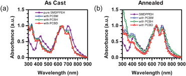 | ||
| Fig. 2 (a) As cast film absorption of pure SMDPPEH (purple stars) and SMDPPEH : PC6161BX (50 : 50) blends and (b) annealed film absorption of SMDPPEH : PC6161BX (50 : 50) blends where X = methyl (blue squares), X = n-hexyl (green circles), and X = n-dodecyl (red diamonds). | ||
Thermally annealing both the pure and as cast films at 100 °C for 5 minutes changes the film absorption spectra significantly (see Fig. 2b). The pure and blended film absorption spectra have become narrow. The “aggregate” absorption maxima in the blended films are now red-shifted relative to the as cast blended films with the λmaxs almost similar to that of the pure SMDPPEH film and, in addition, their intensities are higher than in as cast films. These absorption changes indicate increased crystallinity in both the annealed pure and blended films irrespective of the type of methanofullerene acceptor used.
Thin film XRD was used to determined the differences in crystallinity of the pure and blended films before and after thermal annealing. Fig. 3 gives the diffraction patterns of as cast and annealed pure films and the blends. As seen in Fig. 3a, the pure SMDPPEH film exhibits a peak centered at 2θ = 6.0°, corresponding to an interplanar distance of 14.7 Å. Annealing leads to higher peak intensity, indicating a higher degree of crystallinity. When blended with different fullerene acceptors, this diffraction peak is not observed, suggesting the effectiveness of the fullerene acceptors in interfering with the SMDPPEH molecular packing. This result correlates well with the low peak intensity and blue-shifted absorption characteristics of the “aggregate” species in the blended films (Fig. 2a). Interestingly, when the blends are annealed at 100 °C for 5 minutes, diffraction peaks reappear. The diffraction peak for the SMDPPEH : PC6161BM film is broad and centered at 2θ = 6.2°, corresponding to an interplanar distance of 14.4 Å. In comparison, the peaks for the SMDPPEH : PC6161BH and SMDPPEH : PC6161BD films are sharp and centered at 2θ = 6.0°, corresponding to interplanar distances of 14.7 Å similar to those of the as cast and annealed pure SMDPPEH films. The diffraction intensity is much higher for the SMDPPEH : PC6161BD blend than for those of the SMDPPEH : PC6161BM and SMDPPEH : PC6161BH. These changes in film crystallinity after thermal annealing agree with what is observed in the absorption data.
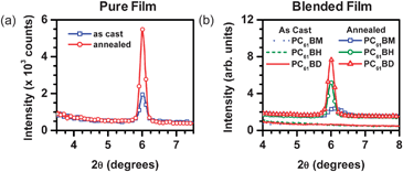 | ||
| Fig. 3 (a) Diffraction patterns for as cast (blue squares) and annealed (red circles) pure SMDPPEH films and (b) diffraction patterns for as cast (lines) and annealed (symbols) SMDPPEH : PC6161BX (50 : 50) blends where X = methyl (blue dotted line and squares), X = n-hexyl (green dashed lines and circles), and X = n-dodecyl (red solid line and triangles). | ||
Depending on the type of derivative, most fullerene acceptors such as PC6161BM do not show any diffraction peaks in the range of 2θ values used.30 The changes in crystallinity of the blended film, therefore, after thermal annealing are mainly attributed to an increase in crystalline domains of the SMDPPEH donor material. Fig. 4a–b show the surface morphology of the pure SMDPPEH film before and after thermal annealing, respectively, obtained using tapping mode AFM. The as cast pure film of donor material is rough (rms = 3.1 nm) and exhibits crystalline domains. Thermally annealing the film increases both the surface roughness (rms = 6.5 nm) and the size of the crystalline domains. This is consistent with the increase in intensity of the diffraction peak as shown in the XRD plots (see Fig. 3a).
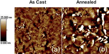 | ||
| Fig. 4 AFM topographic images of (a) as cast and (b) annealed pure SMDPPEH films. Images for both as cast and annealed films are 5 µm × 5 µm in size. | ||
The size of crystalline domains in donor–acceptor films employed in organic solar cells is one of the critical parameters in determining the efficacy of a device. To fabricate efficient BHJ solar cells using SMDPPEH as donor material, it is crucial to develop a method of controlling its tendency to crystallize in the film. Modifying the alkyl solubilizing group attached to the methanofullerenes appears to be an excellent approach to control the extent of crystallization of SMDPPEH and film morphology of the blend.
To examine the effect of using different methanofullerenes on the film morphology of the blend, AFM was employed to probe the film morphological properties of the blended films. The topographic AFM images of the as cast blended films are given in Fig. 5a–c. In all cases, the as cast blended film morphologies are significantly different from that of the as cast pure SMDPPEH film. The as cast blended films are smoother than that of the pure film with an average surface roughness of 0.6 nm, 0.8 nm, and 0.9 nm for the SMDPPEH : PC6161BM, SMDPPEH : PC6161BH, and SMDPPEH : PC6161BD films, respectively. The surface roughness of the film increases slightly as the length of the alkyl chain is increased. In addition, fiber-like structures (Fig. 5a–c) are observed in the as cast blended films and such nanostructures are not observed in the pure film. These fiber-like structures qualitatively increase in domain size with increasing alkyl chain lengths. It is evident from these AFM images that the crystallization of the SMDPPEH donor material in a film is significantly frustrated by the presence of the acceptor material. These observations correlate well with the fact that the as cast blended films do not show any diffraction peak (see Fig. 2b).
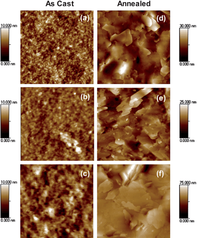 | ||
| Fig. 5 AFM topographic images of as cast (a, b, c) and annealed (d, e, f) SMDPPEH : PC6161BX (50 : 50) from (2% w/v) solution where X = methyl (a and d), X = n-hexyl (b and e), X = n-dodecyl (c and f). Images for the as cast and annealed films are 1 µm × 1 µm and 2 µm × 2 µm in size, respectively. | ||
To examine the thermal stability of the blended films as a function of the alkyl chain length, the blended films were annealed at 100 °C for 5 minutes. Fig. 5d–f shows the topographic images of annealed blended films. The AFM images show that thermal annealing significantly changes the film morphology from fiber-like structures to large crystalline domains with plate-like structures making the film surface rougher. The surface roughness values are 1.5 nm, 3.3 nm, and 8.4 nm for SMDPPEH : PC6161BM, SMDPPEH : PC6161BH, and SMDPPEH : PC6161BD, respectively. Each blended film exhibited various crystalline domain sizes after thermal annealing. The SMDPPEH : PC6161BM film shows small domains (Fig. 5d). Similarly, the domain size in the annealed SMDPPEH : PC6161BD films is increased tremendously and the domains are merged (Fig. 5f). Interestingly, the domain size in the annealed SMDPPEH : PC6161BH film is intermediate to PC6161BM and PC6161BD-based films (Fig. 5e).
To probe further into the morphological properties below the surface of the as cast blended films, TEM was employed. The TEM micrographs of the as cast blended films are given in Fig. 6a–c. Consistent with the AFM studies, fiber-like structures are also observed. The size of the structures increases when the alkyl substituent attached to the methanofullerene is switched from a methyl to hexyl to dodecyl group. Annealing the blended films results in much larger domains, as shown in Fig. 6d–f. These domains are visible in the whole film. Their sizes increase as the length of the alkyl substituent increases. Similar to the AFM results, the annealed SMDPPEH : PC6161BD blended film show merged domains (Fig. 6f). However, no clear phase separation can be observed from TEM images of the annealed blends because one can still observe contrast in isolated domains.
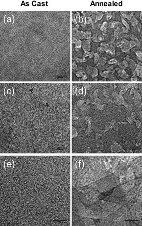 | ||
| Fig. 6 TEM images of as cast (a, b, c) and annealed (d, e, f) blended films of SMDPPEH : PC6161BX (50 : 50) from (2% w/v) solution where X = methyl (a and d), X = n-hexyl (b and e), X = n-dodecyl (c and f). Images for the as cast and annealed films are 0.5 µm × 0.5 µm. | ||
Nevertheless, it is clear from both imaging techniques that the observed fiber-like structures in the as cast and the plate-like structures in the annealed films, and the variation in the domain sizes indicate differences in the degree of intermolecular interactions between the SMDPPEH donor and the methanofullerene acceptors caused by the alkyl chain length. The phase separation depends on the degree of the donor–donor, acceptor–acceptor and donor–acceptor interactions. If the donor–acceptor interaction is stronger than the donor–donor interaction, little phase separation is expected, as in the case of the SMDPPEH : PC6161BM film (Fig. 5a and 6a). For the SMDPPEH : PC6161BD film, large phase separation is observed from both the AFM and TEM images (Fig. 5c and 6c), indicating that the donor–donor and/or acceptor–acceptor interactions are more favorable than the donor–acceptor interaction. It is expected that since the blended films containing PC6161BD already show some phase separation, thermal annealing results in higher degree of phase separation. Because of the weak donor–acceptor interaction, PC6161BD may not effectively prevent the crystallization of SMDPPEH. Crystallization occurs in two steps: nucleation and crystal growth. From the AFM and TEM images, the annealed SMDPPEH : PC6161BM film comprises of higher number of crystalline domains than the SMDPPEH : PC6161BH and the SMDPPEH : PC6161BD films but these domains are much smaller in size, indicating that the nucleation sites are higher. Possibly, the small phase separation in the SMDPPEH : PC6161BM film leads to larger number of nucleation sites. Another possible reason is that the presence of a long alkyl chain on the fullerene interferes with the acceptor crystallization upon thermal annealing, and that the absence of a readily crystallizing acceptor may cause the SMDPPEH molecule to crystallize in larger domains. For the annealed SMDPPEH : PC6161BH film, the extent of phase separation and crystalline domain sizes is expected to fall in between those of the SMDPPEH : PC6161BM and SMDPPEH : PC6161BD films.
To further gain insight into the effect of crystalline domain sizes on the nanoscale charge transport and phase separation upon thermal annealing, C-AFM was used to map out hole conduction/donor domains of as cast and annealed SMDPPEH : PC6161BM and SMDPPEH : PC6161BD. This technique has been successfully used to study nanoscale charge transport in polymer-based devices.31 The current images were collected in the dark using platinum coated silicon tips. Due to the high work function of the nanoelectrode and the conductive substrate, only holes are injected into the blend at a low applied bias (<2 V). Therefore, the high and low current regions correspond to the donor and the acceptor domains, respectively. The current images of the as cast and annealed SMDPPEH : PC6161BM and SMDPPEH : PC6161BD films are shown in Fig. 7a–d. For SMDPPEH : PC6161BM, some high current domains (yellow regions) appear isolated (Fig. 7a); however, upon thermal annealing, these domains disappear and high current networks are distributed throughout the film (Fig. 7b). This result agrees with the device data that annealing SMDPPEH : PC6161BM improves the device efficiency from 2.21% to 2.93% (see Table 1). The current images of the SMDPPEH : PC6161BD show the opposite trend to those of SMDPPEH : PC6161BM. The donor material (yellow region) is well distributed before annealing but undergone a large phase separation after annealing. This large phase separation leads to devices with lower efficiencies (from 2.63% to 1.49%, Table 1). The phase separation of the SMDPPEH : PC6161BH film falls in between those of the SMDPPEH : PC6161BM and SMDPPEH : PC6161BD films. The increased crystallinity in annealed SMDPPEH : PC6161BM and SMDPPEH : PC6161BD films also reflects through the double hole current level in the current images (Fig. 7b and 7d). We expect that these differences in film morphology in as cast and annealed blended films will have a significant impact on the device performance as discussed below.
| As cast film | J SC/mA cm−2 | V OC/volts | FF | PCE (%) |
|---|---|---|---|---|
| PC6161BM | 7.87 | 0.77 | 0.36 | 2.21 |
| PC6161BH | 7.82 | 0.77 | 0.40 | 2.41 |
| PC6161BD | 6.96 | 0.83 | 0.45 | 2.63 |
| Annealed Film | ||||
| PC6161BM | 8.06 | 0.80 | 0.45 | 2.93 |
| PC6161BH | 6.39 | 0.87 | 0.50 | 2.79 |
| PC6161BD | 3.38 | 0.90 | 0.48 | 1.49 |
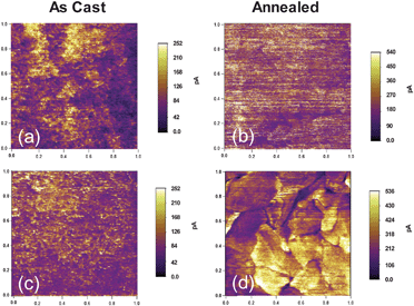 | ||
| Fig. 7 C-AFM current images of as cast (a, c) and annealed (b, d) SMDPPEH : PC6161BX (50 : 50) from (2% w/v) solution where X = methyl (a and b), and X = n-dodecyl (c and d). Images for the as cast and annealed films are 1 µm × 1 µm in size. | ||
SMDPPEH-based solar cells were fabricated using 50 : 50 donor–acceptor blend ratio to examine the influence of the alkyl side chains attached on the methanofullerene acceptors on device performance. Fig. 8a shows the current density versus voltage (J–V) characteristics for devices using a 50 : 50 blend ratio SMDPPEH : PCBX (where X = alkyl chain). A summary of the device properties is given in Table 1. All the as cast devices have similar open-circuit voltages (VOC = 0.77 V–0.83 V) independent of the alkyl chain attached to the methanofullerene. Since the VOC in BHJ solar cells mainly arises from the difference between the energy of the highest occupied molecular orbital (HOMO) of the donor and lowest unoccupied molecular orbital (LUMO) of the acceptor, then the measured VOC values for the as cast devices indicate similar LUMO energies for the three methanofullerenes. This is consistent with only small variations in the LUMO energies measured for this class of methanofullerene acceptors using cyclic voltammetry.19–21 The short-circuit current densities (JSC) show a slight dependence on the alkyl chain length. The JSCs decrease from 7.87 mA cm−2 to 7.82 mA cm−2 to 6.96 mA cm−2 when the acceptor is changed from PC6161BM to PC6161BH to PC6161BD, respectively. In contrast, the fill-factors (FFs) show the opposite trend increasing from 36% to 40% to 45% in the same series, resulting in increased power conversion efficiencies (PCEs) with PC6161BD giving the highest PCE of 2.63%. For the as cast devices, no significant difference in the external quantum efficiency (EQE) spectra is observed (Fig. 8c). All devices show that the donor and acceptor contribution in the EQE spectra are qualitatively similar (peaks at 620 nm and 710 nm for donor and peak at ∼440 nm for acceptor). The methanofullerene acceptors all give a 30% contribution and 40–45% from the donor in the as cast devices irrespective of the alkyl substituent. Overall, the slight differences in device performance measured for the as cast devices are consistent with the differences in film morphology of the as cast blended films.
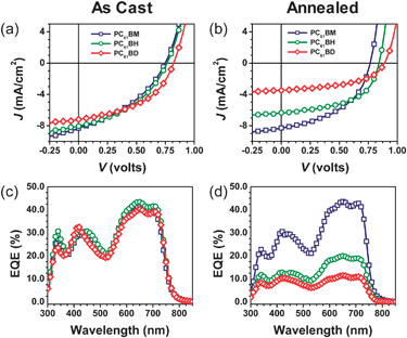 | ||
| Fig. 8 (a,b) Current density–voltage characteristics and (c,d) EQEs of SMDPPEH : PC6161BX BHJ solar cells as a function of alkyl substituent and thermal annealing at 100 °C where X = methyl (blue squares), X = n-hexyl (green circles), and X = n-dodecyl (red diamonds). | ||
The device performances are significantly altered after thermal annealing as shown in Fig. 8b. These alterations correlate well to the significant changes in the morphologies of the blended films. The VOC of the SMDPPEH : PC6161BD device increases slightly upon thermal annealing reaching the value of 0.9 V, but its JSC decreases tremendously from 6.96 mA cm−2 to 3.38 mA cm−2 (Table 1). As a result, the PCE for the annealed device drops from 2.63% to 1.49%, mainly due to a significant loss in the measured short-circuit current density, a consequence of a larger degree of phase separation which is confirmed by C-AFM measurement (Fig. 7c and 7d). For the annealed SMDPPEH : PC6161BM device, VOC and JSC increase slightly by ∼0.03 V and 0.2 mA cm−2, respectively. FF improves significantly from 0.36 to 0.45 resulting in a PCE improvement of 33% (from 2.21% to 2.93%). In contrast, JSC for the SMDPPEH : PC6161BH device reduces from 7.82 mA cm−2 to 6.39 mA cm−2 upon thermal annealing, but at the same time VOC and FF increased to 0.87 V (from 0.77 V) and to 0.50 (from 0.40), respectively. Thus, the overall device PCE for PC6161BH increased from 2.41% to 2.79% after thermal annealing (Table 1). The difference in the device performance observed is mainly due to a change in film morphology because the three fullerene derivatives used here have a similar LUMO value.20,21,32
Although qualitatively similar, the measured EQE spectra for the thermally annealed devices are very different and dependence on the nature of the alkyl chain attached to the methanofullerene is apparent with the devices using PC6161BH and PC6161BD, having less donor and acceptor contribution to the photocurrent relative to the devices using PC6161BM. The changes in the EQE spectra of the annealed devices are consistent with both changes in the blend optical properties as well as morphological changes that lead to poor charge separation and transport in the annealed films. The increase in film roughness and the large phase separation observed in the annealed films as seen in AFM, TEM, and conducting AFM lead to inefficient charge transfer process. In the case of the SMDPPEH : PC6161BH device, both an increase in the film roughness and phase separation result in a small drop in the JSC. However, this drop in JSC is accompanied by an increase in the FF which can indicate better charge collection in the annealed device. In contrast, the annealed SMDPPEH : PC6161BD devices gave PCEs of 1.49% from a high of 2.63%, mainly due to a larger drop in the JSC. This is because a higher degree of phase separation (Fig. 7d) is observed in these films after annealing compared to the degree of phase separation in the annealed SMDPPEH : PC6161BH and SMDPPEH : PC6161BM systems. As for the annealed SMDPPEH : PC6161BM devices, less phase separation is observed from the conducting AFM data (Fig. 7b) relative to the other systems. The increase in performance is likely due to a better charge collection as a result of the formation of crystalline domains that are somewhat ideal for both charge separation and collection. This is supported by the almost two-fold increase in the current measured in the annealed blended film using C-AFM (Fig. 7b). From these results, one observes that some degree of phase separation is good for solar cells; however, large scale phase separation results in inefficient devices due to a decreased interfacial contact area between donor and acceptor domains and resulting in poor electron transfer. It has been shown in both small molecule and polymer-based BHJ solar cells that the degree of phase separation and surface roughness in blended films significantly affect the efficiency of electron transfer, charge transport, and charge carrier collection.7,33,34 It is speculated that similar processes are at work in these systems.
Conclusions
Achieving an ideal morphology is crucial to the performance and stability of BHJ solar cells and requires tuning the intermolecular interactions between the donor and acceptor components in the blended film. The as cast pure film of the donor material studied here shows crystalline domains that increase in size after thermal annealing. The extent of its crystallization can be controlled by blending with methanofullerene acceptors. The crystallinity and morphology of the as cast blended films were found to be significantly different from that of the pure film giving fiber-like structures. The domain size of these structures increase as the alkyl chain attached to the methanofullerene acceptor is increased. Annealing the blended films leads to varying degrees of phase separation in the film. The largest phase separation is observed with the methanofullerene having a dodecyl side chain. These observations have been attributed to the differences in hydrophobicity of the methanofullerenes, which affects their interaction with the relatively more polar donor material. The result of these interactions lead to efficient as cast devices when they are favorable and very poor annealed devices when they detrimental. This direct dependence on the length of the alkyl chain attached to the methanofullerene of solution processed small molecule BHJ solar cells is in contrast to similar studies using polymeric donor materials, where minimal changes in phase behavior are observed in both as cast and annealed devices. Further improvements in device performance will require continued investigation into how the nature of various functional groups attached to either donor and acceptor components affect the film morphology of the device active layer.This work is supported by the Office of Naval Research, the Department of Energy, and the Camille Dreyfus Teacher Scholar Award program. T.-Q. N. is an Alfred P. Sloan Foundation Research Fellow. A. T. thanks Jeff Peet for helpful discussions. J. R. thanks ConvEne IGERT Program (NSF-DGE 0801627) for support.
References
- G. Dennler, M. C. Scharber and C. J. Brabec, Adv. Mater., 2009, 21, 1323–1338 CrossRef CAS.
- B. C. Thompson and J. M. J. Frechet, Angew. Chem., Int. Ed., 2008, 47, 58–77 CrossRef.
- C. J. Brabec and J. R. Durrant, MRS Bull., 2008, 33, 670–675 CAS.
- J. Peet, J. Y. Kim, N. E. Coates, W. L. Ma, D. Moses, A. J. Heeger and G. C. Bazan, Nat. Mater., 2007, 6, 497–500 CrossRef CAS.
- J. Y. Kim, K. Lee, N. E. Coates, D. Moses, T.-Q. Nguyen, M. Dante and A. J. Heeger, Science, 2007, 317, 222–225 CrossRef CAS.
- S.-S. Kim, S.-I. Na, J. Jo, G. Tae and D.-Y. Kim, Adv. Mater., 2007, 19, 4410–4415 CrossRef CAS.
- T. M. Lloyd, J. E. Anthony and G. G. Malliaras, Mater. Today (Oxford, U. K.), 2007, 10, 34–41 CrossRef CAS.
- C.-Q. Ma, M. Fonrodona, M. C. Schikora, M. M. Wienk, R. A. J. Janssen and P. Bauerle, Adv. Funct. Mater., 2008, 18, 3323–3331 CrossRef CAS.
- M. T. Lloyd, A. C. Mayer, S. Subramanian, D. A. Mourey, D. J. Herman, A. V. Bapat, J. E. Anthony and G. G. Malliaras, J. Am. Chem. Soc., 2007, 129, 9144–9149 CrossRef.
- N. Kopidakis, W. J. Mitchell, J. van de Lagemaat, D. S. Ginley, G. and S. E. Shaheen, Appl. Phys. Lett., 2006, 89, 103524 CrossRef , (1–3).
- L. Schmidt-Mende, A. Fechtenkötter, K. Müllen, E. Moons, R. H. Friend and J. D. MacKenzie, Science, 2001, 293, 1119–1122 CrossRef CAS.
- J. L. Li, M. Kastler, W. Pisula, J. W. F. Robertson, D. Wasserfallen, A. C. Grimsdale, J. S. Wu and K. Mullen, Adv. Funct. Mater., 2007, 17, 2528–2533 CrossRef CAS.
- Y. Kim, S. Cook, S. M. Tuladhar, S. A. Choulis, J. Nelson, J. R. Durrant, D. D. C. Bradley, M. Giles, I. McCulloch, C.-S. Ha and M. Ree, Nat. Mater., 2006, 5, 197–203 CrossRef CAS.
- W. Ma, J. Y. Kim, S. K. Lee and A. J. Heeger, Macromol. Rapid Commun., 2007, 28, 1776–1780 CrossRef CAS.
- M. Muccini, Nat. Mater., 2006, 5, 605–613 CrossRef CAS.
- Y-Lin Loo, AIChE J., 2007, 53, 1066–1074 CrossRef CAS.
- M. A. Loi, E. Da Como, F. Dinelli, M. Murgia, R. Zamboni, F. Biscarini and M. Muccini, Nat. Mater., 2005, 4, 81–85 CrossRef CAS.
- L. H. Nguyen, H. Hoppe, T. Erb, S. Gunes, G. Gobsch and N. S. Sariciftci, Adv. Funct. Mater., 2007, 17, 1071–1078 CrossRef CAS.
- H.-J. Lee, T. Arai, Y. Takeuchi, N. Koide, L. Han and M. Shimizu, IEEE (Photovoltaic Energy Conversion, Conference Record of the 2006 IEEE 4th World Conference), 2006, 1, 233–235 Search PubMed.
- L. Zheng, Q. Zhou, X. Deng, M. Yuan, G. Yu and Y. Cao, J. Phys. Chem. B, 2004, 108, 11921–11926 CrossRef CAS.
- C.-H. Yang, J.-Y. Chang, P.-H. Yeh and T.-Z. Guo, Carbon, 2007, 45, 2951–2956 CrossRef CAS.
- P. A. Troshin, H. Hoppe, J. Renz, M. Egginger, J. Y. Mayorova, A. E. Goryachev, A. S. Peregudov, R. N. Lyubovskaya, G. Gobsch, N. S. Sariciftci and V. F. Razumov, Adv. Funct. Mater., 2009, 19, 779–788 CrossRef CAS.
- M. R. Reyes, K. Kim and D. L. Caroll, Appl. Phys. Lett., 2005, 87, 083506 CrossRef (1–3).
- W. Ma, C. Yang, X. Gong, K. Lee and A. J. Heeger, Adv. Funct. Mater., 2005, 15, 1617–1622 CrossRef CAS.
- Y. Kim, S. A. Choulis, J. Nelson, D. D. C. Bradley, S. Cook and J. R. Durrant, Appl. Phys. Lett., 2005, 86, 063502 CrossRef (1–3).
- D. Muhlbacher, M. Scharber, M. Morana, Z. Zhu, D. Waller, R. Gaudiana and C. Brabec, Adv. Mater., 2006, 18, 2884–2889 CrossRef.
- A. B. Tamayo, X.-D. Dang, T. Kent, B. W. Walker and T.-Q. Nguyen, Appl. Phys. Lett., 2009, 94, 103301 CrossRef (1–3).
- A. B. Tamayo, M. Tantiwiwat, B. W. Walker and T.-Q. Nguyen, J. Phys. Chem. C, 2008, 112, 15543–15552 CrossRef CAS.
- H. Hoppe and N. S. Saricitci, J. Mater. Chem., 2006, 16, 45–61 RSC.
- M. Chikamatsu, S. Nagamatsu, Y. Yoshida, K. Saito and K. Yase, Appl. Phys. Lett., 2005, 87, 203504 CrossRef (1–3).
- M. Dante, A. Garcia and T.-Q. Nguyen, J. Phys. Chem. C, 2008, 112, 7241–7249 CrossRef CAS.
- S. A. Backer, K. Sivula, D. F. Kavulak and J. M. J. Frechet, Chem. Mater., 2007, 19, 2927–2929 CrossRef CAS.
- H. Hoppe, M. Niggemann, C. Winder, J. Kraut, R. Hiesgen, A. Hinsch, D. Meissner and N. S. Sariciftci, Adv. Funct. Mater., 2004, 14, 1005–1011 CrossRef CAS.
- X. Yang, J. Loos, S. C. Veenstra, W. J. H. Verhees, M. M. Wienk, J. M. Kroon, M. A. J. Michels and R. A. J. Janssen, Nano Lett., 2005, 5, 579–5833 CrossRef CAS.
| This journal is © The Royal Society of Chemistry 2009 |
