Nanoscale optoelectronic switches and logic devices
Sylwia
Gawęda
a,
Agnieszka
Podborska
a,
Wojciech
Macyk
a and
Konrad
Szaciłowski
*ab
aUniwersytet Jagielloński, Wydział Chemii, ul. Ingardena 3, 30-060, Kraków, Poland. E-mail: szacilow@chemia.uj.edu.pl
bAkademia Górniczo-Hutnicza, Wydział Metali Nieżelaznych, al. Mickiewicza 30, 30-059, Kraków, Poland. E-mail: szacilow@agh.edu.pl
First published on 22nd October 2009
Abstract
The photoelectrochemical photocurrent switching (PEPS) effect, in the beginning regarded as a scientific curiosity, has become a field of extensive study for numerous research groups all over the world. This unique effect can be utilized for nanoscale switching and information processing, furthermore, is can serve as an interface between molecular information processing and macroscopic electronics. This review summarizes recent efforts in understanding photocurrent switching effects and their application for the construction of nanoscale switches and logic devices. Furthermore, some future prospects concerning the development of electronic/optoelectronic devices based on photoactive semiconducting hybrid materials are presented.
 Wojciech Macyk; Sylwia Gawęda; Agnieszka Podborska; Konrad Szaciłowski. | Sylwia Gawęda (upper right) was born in Kraków, Poland in 1981. She graduated from Jagiellonian University in 2005—MSc degree in Chemistry, specialization biological chemistry. She is currently working toward her PhD degree under the supervision of Professor Grażyna Stochel and in collaboration with Dr Konrad Szaciłowski in the Coordination and Bioinorganic Physicochemistry Group at the Faculty of Chemistry of the Jagiellonian University. During her PhD studies she spent a few months in Professor M. Graca Miguel’s group at the University of Coimbra in Portugal working on DNA compaction. Now her research interests encompass spectroscopy of nanoparticles, photosensitization and photoelectrochemistry of wide-band-gap semiconductors. |
Agnieszka Podborska (lower left) received her MSc (Chemistry) degree from Jagiellonian University (Kraków, Poland) in 2007. Now she is working towards her PhD degree under the guidance of Dr Konrad Szaciłowski in Coordination and Bioinorganic Physicochemistry Group. Her research interests are focused on synthesis and photoelectrochemistry of nanocrystalline wide band gap semiconductors, photoelectrochemical photocurrent switching effect in modified semiconductors, logic gates and optoelectronic devices. |
Wojciech Macyk (upper left) graduated from the Jagiellonian University, Kraków, Poland (1997), he completed PhD studies at the University of Erlangen-Nürnberg, Germany, in the group of Professor Horst Kisch (2000). Since 2002 he has worked at the Faculty of Chemistry, Jagiellonian University, where he completed his habilitation in 2009. His research interests include heterogeneous photocatalysis (especially TiO2 photosensitization and singlet oxygen generation at wide-band-gap semiconductors), photocatalytic detoxification and disinfection, as well as photoelectrochemistry of nanocrystalline semiconductors. He was awarded the Albert Weller Prize and the Staedtler Prize, in addition to the fellowships from the Foundation for Polish Science and Polityka magazine. |
Konrad Szaciłowski (lower right) was born in Kraków, Poland in 1971. He graduated from Jagiellonian University in 1995 and got his PhD degree in 2000. He spent one year as a postdoc fellow with Professor John F. Endicott working on spectroscopy and magnetism of binuclear nickel compounds. After habilitation in 2008 he was appointed as a professor of inorganic chemistry at AGH University of Science and Technology. He is also a member of Photochemistry of Coordination Compounds and Bioinorganic Chemistry Group at Jagiellonian University. His research interests are focused mainly on information processing at molecular level, surface engineering of nanocrystalline materials, (photo)electrochemistry of wide band gap semiconductors, and molecular nanoelectronics. Currently he is also working on electrodeposition of semiconducting films for chemosensors and optoelectronic devices. |
1. Introduction
Processes of energy and information conversion are the most basic phenomena in nature. Various molecular and nanoscopic assemblies try to simulate the behavior of natural systems. Light-harvesting antennae, photovoltaic cells, artificial neuron-like systems and molecular logic gates are the best examples of bioinspired devices performing energy/information processing.1,2Modern society requires more and more powerful computing devices. Classical semiconductor devices have almost reached their technological limits3–7 and alternative information processing technologies are being extensively researched.8–15 The application of molecular devices may contemporarily solve the problems.1,16–21 These systems are, however, in most cases based on fluid solutions. While information is being processed at the nanoscale, the issues to be addressed are serious. By no means one can address a selected molecule in a droplet of liquid. It is, however, much more probable if the molecules are immobilized on solid substrates that keep all of them in a pre-organized arrangement.22 These systems offer a higher mechanical and chemical stability together with a better addressability and controlled interaction between individual molecular-scale devices. In fluid solutions the number of independent switches/logic gates is limited by the number of distinctly different chemical species used for information transfer between various gates,23 while at solid surfaces it is limited mostly by our skills to address them and/or read information out of them. Furthermore, the application of light as the information carrier may further improve the performance of molecular-scale devices and eliminate the inter-channel crosstalk, which is a serious problem arising from the downscaling of classical electronic devices. One of the phenomena that can make use of both optical and electrical signals is the photoelectrochemical photocurrent switching (PEPS) effect. This effect can be defined as switching of photocurrent polarity on changes in photoelectrode potential and/or incident light wavelength.
This review article is focused mostly on photoelectrochemical switching processes occurring at solid–liquid interfaces and in thin films and monomolecular layers. While addressing single nanoparticles/molecules is still a nontrivial process, the observed switching phenomena occur at the single molecule/nanoparticle level, as the mechanisms do not involve any inter-particle interactions.
2. Organic thin-layer photodiodes and related devices
Diodes are the simplest active electronic components. A diode is an element based on a single p–n junction. In classical semiconductor technology they are formed by the appropriate doping of a silicon wafer to generate neighboring electron-rich and electron-depleted areas and all other, more complex elements (bipolar transistors, thyristors, diacs and triacs) can be regarded as multidiode (i.e. multijunction) devices.24 Furthermore, logic gates can be constructed exclusively from diodes and resistors using a diode–resistor logic approach.25 While the logic devices based on diodes are very simple, they operate in a non-restoring regime (i.e. the input voltage is used to drive the output), neither signal inversion nor amplification is possible, and each p–n junction adds extra noise to the processed signals. This simplicity, however, makes the diode–resistor logic the best candidate to implement in molecular systems.26Molecular diodes (rectifiers) were first postulated in the mid-seventies by Arieh Aviram and Mark A. Ratner27 (Fig. 1) and since that time numerous materials based on donor–spacer–acceptor architectures have been reported and used in various molecular-scale devices.28 These systems were based on a donor–spacer–acceptor framework, which is the molecular-scale equivalent of a p–n junction, as electron donors mimic the n-type semiconductor, electron acceptors the p-type semiconductor and the σ-spacer is equivalent to the space-charge layer at the p–n junction. In molecular systems there are three different possibilities for constructing rectifying p–n junctions: integration of donor and acceptor moieties within the same molecule,29–31 contacting of donor and acceptor layers (planar heterojunctions)32–34 and blending electron donor and acceptor molecules in a polymeric matrix (bulk heterojunctions).35–37 While the monomolecular devices are not fully understood up to now, the latter planar and bulk heterojunction materials have already found applications in OLED devices and organic solar cells. These applications rely on a high efficiency of radiative electron–hole recombinations and photoinduced charge separations, respectively.38 Apart from these rather obvious applications, heterojunction molecular materials have been successfully used for the construction of prototypical information-processing devices. Furthermore, self-organization and self-assembly of these organic materials render them prospective successors of silicon semiconductor devices.37,39–48 Various organic and metalloorganic supermolecules can be used as interconnects between individual molecular devices.49–52
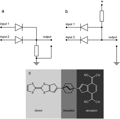 | ||
| Fig. 1 Schematics of diode–resistor-based (a) OR and (b) AND logic gates and the first predicted molecular rectifier: the Aviram–Ratner Gedankenmolekül (c). Adapted from refs. 26 and 27. | ||
The very first molecular photodiodes created for digital information processing were based on Langmuir–Blodgett (LB) biomimetic films.53 In the initial stages of a photosynthetic reaction photoexcited molecules undergo long-range electron transfer. The same processes can be observed in various donor–acceptor molecular systems equipped with an efficient chromophore.54 The first potential-controlled photodiode was composed of three molecular components: tetracyanoquinodimethane (electron acceptor), ferrocene (electron donor) and pyrene (photonic antenna), each of them was additionally equipped with a long aliphatic chain to facilitate LB deposition. The tetracyanoquinodimethane (TCNQ) layer was deposited on a conducting substrate (ITO-covered glass), other components were deposited subsequently, while the donor layer was coated with a thin aluminium film. Thus prepared metal–insulator–metal (MIM) structure generated photocurrent upon illumination with UV light, photocurrent intensity strongly depended on the bias potential applied between the two conducting electrodes (Fig. 2a). Forward polarization of the device resulted in photocurrent generation while at reverse polarization a much weaker response was observed. Excitation of the pyrene chromophore results in photoinduced electron-transfer from the ferrocene donor moiety and subsequently the electron is captured by the TCNQ acceptor (Fig. 2b). Much better performance was observed when an additional layer of electron acceptor was added. Related devices were based on layers of ferrocene (donor), flavin (photosensitizer), viologen (primary electron acceptor) and TCNQ (final electron acceptor).55 Various biomolecules (e.g.cytochrome c56,57 or green fluorescent protein57) can be used as electron acceptors or photonic antennae, respectively.
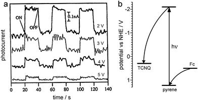 | ||
| Fig. 2 Photocurrent response (a) and energy diagram (b) for a LB MIM device composed of alkyl derivatives of tetracyanoquinodimethane (TCNQ), pyrene and ferrocene (Fc) at various bias voltages. Adapted from ref. 53. | ||
MIM architectures have been successfully used for the construction of prototypical AND58 and OR59 logic gates using the diode–diode logic approach. Both devices consisted of two MIM photodiodes connected in parallel (cf.Fig. 1). In the case of the AND gate the high output photocurrent (logic 1) was observed only in the case of excitation of both photodiodes (i.e. [1,1] input state), while illumination of one photodiode (input states [0,1] and [1,0]) resulted in low-intensity photocurrents. The OR function was implemented in a similar way, but with a different bias voltage and different photocurrent threshold values.
The power and versatility of MIM-type devices is embodied by the very recent discovery of a memristor. The memristor is the fourth basic passive element (other basic elements are resistor, capacitor and inductor), first predicted theoretically by Leon Chua in 1971.60 Memristive behavior was found in very thin layers of TiO2 sandwiched between platinum electrodes.61 The memory effects and switching of the electric conductivity of the TiO2 layer results from potential-induced dynamic doping and de-doping of the semiconductor. While these memristors do not utilize light for their operation, application of a photoactive material suggests the possibility of further development of these unique electronic elements. Also, other semiconducting materials have been used in novel memory devices based on electric-field-induced changes in conductivity.62–67
Most of the other molecular optoelectronic switches operating by photocurrent switching were based on a three-electrode setup in a liquid electrolyte. These devices were composed of a working electrode containing molecular or semiconducting mono- or multilayers immersed in aqueous electrolyte. These photoelectrodes can be regarded as multilayer molecular photodiodes (or circuits consisting of several photodiodes). The auxiliary electrode was used to close the circuit, while external polarization of the working electrode was determined using the reference electrode.
A versatile photoelectrochemical logic device was reported in 2003 by Tokuji Miyashita and co-workers.68 These devices were based on multilayer polymeric structures deposited onto gold substrates. The Langmuir–Blodgett layers of tert-pentaacrylamide, covalently modified with various molecular species, served as light absorbers and charge-separating systems (electron donors and electron acceptors), while photocurrent generation and polarity was controlled by selective excitation of dye molecules embedded in a polymeric matrix. Dimethylaniline and dinitrobenzoate moieties served as electron donors and acceptors, respectively, while anthracene and phenanthrene moieties were primary light absorbers. Depending on the sequence of layers, photoelectrodes can yield various photoelectrochemical responses. A device consisting of two chromophoric layers (phenanthrene and anthracene) separated by donor and acceptor layers, operates as an optoelectronic AND gate. Excitation of whichever chromophore results in a weak cathodic photocurrent due to photoinduced electron transfer from phenanthrene to the electron acceptor or from the electron donor to anthracene moieties. Simultaneous excitation of both chromophores results in a photocurrent of intensity much higher than the sum of photocurrents recorded upon a single chromophore excitation. This increase results from a dual role of donor and acceptor thin layers: apart from the charge generation they contribute to the charge transport. The mechanism of operation of this device is shown in Fig. 3a.
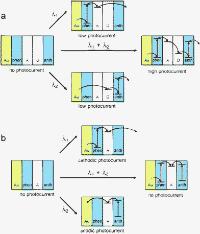 | ||
| Fig. 3 Mechanism of operation of the photoelectrochemical AND (a) and XOR (b) photoelectrochemical logic gates. (Au – gold substrate, phen – phenanthrene-doped polymer, A – acceptor polymer, D – donor polymer, anth – anthracene-doped polymer). Adapted from refs. 68 and 69 and reproduced from ref. 1 with permission. Copyright American Chemical Society 2008. | ||
Another thin-layer molecular photodiode-like structure can operate as the photoelectrochemical XOR gate (Fig. 3b).69 In this device an electron-acceptor layer is sandwiched between two chromophoric layers. Excitation of any of the chromophores results in a photoinduced electron transfer from the excited chromophore to the electron acceptor. The photocurrent polarity depends on the geometrical arrangement of these layers: excitation of the surface layer results in an anodic photocurrent, while excitation of the layer being in contact with a conducting support – in a cathodic photocurrent. Concomitant irradiation of both chromophoric layers results in null net photocurrent as both signals (cathodic and anodic photocurrents) compensate. This behavior corresponds to the XOR function (Fig. 3b).
The same approach was later explored by Kimura et al.70 The switchable gold photoelectrodes were decorated with helical oligopeptide chains with ruthenium bipyridine and carbazolechromophores. Furthermore, like in the previous case, the electrolyte contained the electron donor (triethanolamine) and electron acceptor (methyl viologen). Excitation of ruthenium centers resulted in the reduction of methyl viologen and the generation of cathodic photocurrents, while photoexcited carbazole moieties oxidized triethanolamine and induced the generation of anodic photocurrents. A small modification of the carbazolechromophore (introduction of one unprotected carboxylic group) results in a system capable of photocurrent polarity modulation by pH of the electrolyte.71 The protonated form of the peptide generates cathodic photocurrents due to a photoinduced electron transfer from the carbazole moiety to methyl viologen. Deprotonation generates an additional charge localized in the vicinity of the chromophore and promotes electron transfer towards the conducting support. The devices based on helical peptides yield very low photocurrent intensities (50–100 pA).70 Furthermore, their operation can be strongly perturbed by the photoelectrochemical response resulting from a local heating of chromophore-modified gold surface, so the reliability of the device is highly questionable, since very similar effects can be observed even at neat gold surfaces.72
Another device responding exclusively to various chemical signals was reported very recently by Nakamura et al.73 The switching system was based on self-assembled monolayers of pentaaryl[60]fullerene derivatives equipped with various anchoring groups (Fig. 4a,b). While the pentacarboxylic anchor (Fig. 4a) generated a strong electric field, stabilizing only anodic photocurrent, the single phosphonate anchor (Fig. 4b) allowed efficient photocurrent switching induced by sacrificial reagents present in the electrolyte. 400-nm irradiation of fullerene-derivative monolayers in the presence of a sacrificial electron donor (ascorbic acid in water or triethanolamine in acetonitrile) resulted in anodic photocurrents. The singlet excited state undergoes intersystem crossing quickly and efficiently, yielding the triplet excited state. This state is a rather strong oxidizing agent, easily abstracting one electron from sacrificial reducing agents. This process generates in turn, a fulleride radical anion which injects an electron into a conducting metal oxide (ITO or SnO2) (Fig. 4c). In the presence of efficient electron acceptors, the 3C60 excited state can adopt one electron from the electrode and the resulting C60− anion donates an electron to the sacrificial acceptor (Fig. 4d) thus generating a cathodic photocurrent.
![Schematic representation of self-assembled monolayers of pentaaryl[60]fullerenes on ITO surfaces: penta(biphenyl)[60]fullerene pentacarboxylic acid (a) and penta(biphenyl)[60]fullerenylhexanephosphonic acid (b) together with mechanisms of anodic (c) and cathodic (d) photocurrent generation by phosphonic derivatives at the potential of 0 V vs the Ag/AgCl reference. Adapted from ref. 73 with permission.](/image/article/2009/NR/b9nr00145j/b9nr00145j-f4.gif) | ||
| Fig. 4 Schematic representation of self-assembled monolayers of pentaaryl[60]fullerenes on ITO surfaces: penta(biphenyl)[60]fullerene pentacarboxylic acid (a) and penta(biphenyl)[60]fullerenylhexanephosphonic acid (b) together with mechanisms of anodic (c) and cathodic (d) photocurrent generation by phosphonic derivatives at the potential of 0 V vs the Ag/AgCl reference. Adapted from ref. 73 with permission. | ||
Yamada et al. have reported another optically switchable device yielding much higher photocurrent intensities as compared to the previous cases (Fig. 5).74,75 Gold photoelectrodes have been modified with mixed monolayers of two chromophores anchored via sulfur-terminated alkyl chains: palladium(II) phthalocyanine and the [Ru(bpy)3]2+ complex with one ligand additionally substituted with a viologen moiety (Fig. 5a). Due to the significantly different absorption spectra of these two chromophores they can be independently addressed with light of a suitable wavelength: blue light is absorbed mainly by the ruthenium bipyridine complex, while red light – by the palladium phthalocyanine. Excitation of the ruthenium complex induces electron transfer from the excited ruthenium species towards the viologen moiety, which in turn can be reoxidized by the electrode, while the ruthenium complex is regenerated by the sacrificial electron donor (triethanolamine). This process is responsible for anodic photocurrent generation (Fig. 5b). A cathodic photocurrent is in turn generated upon excitation of palladium phthalocyanine with red light in the presence of a sacrificial electron acceptor (e.g.methyl viologen, Fig. 5c). Therefore, blue light generates anodic photocurrents while red light – cathodic photocurrents. Concomitant excitation with blue and red light results in null net photocurrent due to a complete compensation of anodic and cathodic photocurrents. Such behavior corresponds to the XOR gate.
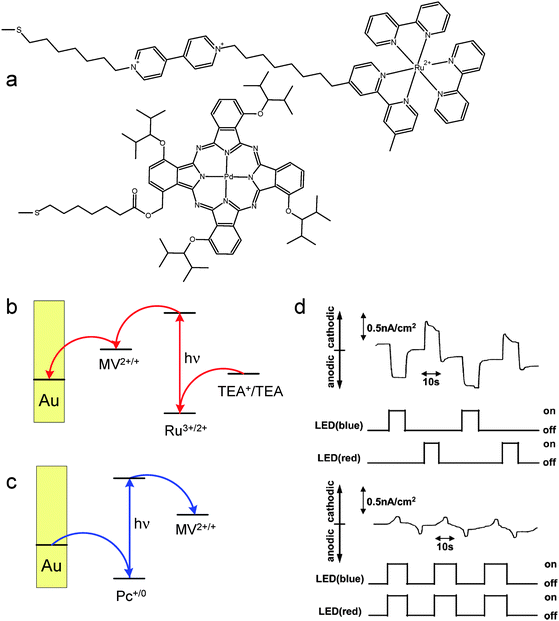 | ||
| Fig. 5 (a) Molecular structures of components of the photoelectrochemical switch, mechanisms of generation of anodic (b) and cathodic (c) photocurrents and photoelectrochemical characteristics of the device (d). (TEA – triethanolamine, MV2+ – methyl viologen cation, Pc – phthalocyanine). Adapted from refs. 74 and 75 and reproduced from ref. 1 with permission. Copyright American Chemical Society 2008. | ||
Organic thin-layer optoelectronic switches offer a great structural versatility and the possibility of an almost infinite combination of chromophores, donors and acceptors. However, due to a relatively low carrier mobility (in the order of 10−3 cm2 V−1 s−1) in these materials, and low local concentration of chromophores (monomolecular layer), the photocurrent generated in these devices are very low (≤ 1nA) and thus difficult to follow. Furthermore, in the presence of electrolytes they are susceptible to a rapid photodegradation due to the photocatalytic properties of conjugated chromophores. The MIM devices are free of the last drawback, but the current densities offered by these structures are also very low (∼1 nA mm−2).67
3. Surface-modified semiconductors
Surface-modified semiconductor materials are of central importance due to their versatility, stability and performance. The photoelectrochemical properties of nanocrystalline semiconducting systems are especially promising as platforms for imitating natural energy and information processing. A surface modification of semiconductors has been shown to be a powerful technique for tuning their electronic and optical properties.Surface modification of wide-band-gap semiconductors (TiO2, CdS) results in materials with unique properties. The surface of titanium dioxide and other semiconductors can be easily modified with organic, organometallic or inorganicchromophores to yield materials suitable for solar energy harvesting and other photoelectrochemical applications.76,77 This energy can be further utilized for electric energy generation (photovoltaics), information processing (molecular optoelectronics), and driving chemical reactions (photocatalysis).78–81
Systems based on nanostructured wide-band-gap semiconductors surface-modified with various compounds present unique photoelectrochemical properties and are characterized by means of optical spectroscopy , electrochemistry and photoelectrochemistry. Systems exhibiting pronounced photocurrent switching (PEPS effect) are selected for construction of prototypical optoelectronic switches, logic gates and more complex logic devices.
3.1. Modes of sensitization
The properties of the surface-modified semiconductor can be described by quantum chemical tools based on the interaction between isolated electronic levels of the surface molecule (especially HOMO and LUMO orbitals) and the electronic continuum of the semiconducting support under the influence of a radiation field.82–85 The total Hamiltonian of the system (Ĥ) can be thus regarded as a sum of Hamiltonians for all components (Ĥ0) and a coupling operator including all the physical processes of interest (Ŵ) (eqn (1)):| Ĥ = Ĥ0 + Ŵ | (1) |
The Ĥ0 Hamiltonian is a sum of the Hamiltonians for the isolated molecule ĤM, the semiconducting substrate ĤS and the radiation field ĤR(eqn (2)),
| Ĥ0 = ĤM + ĤS + ĤR | (2) |
| Ŵ = ŴET + ŴDC + ŴRM + ŴRS + ŴRMS | (3) |
This sum includes terms describing the following processes: electron transfer coupling between each isolated molecular electronic state of the surface moiety and the electronic continuum of the semiconductor (ŴET); dipole-induced dipole coupling (energy transfer), which describes an interaction of the excited molecule and the dielectric response of the support (ŴDC); molecule–radiation field coupling describing light absorption by the isolated molecule (ŴRM); semiconductor–radiation field coupling depicting the optical properties of the semiconductor (ŴRS); and molecule–semiconductor–radiation field coupling, which describes a direct electronic transition between the semiconductor electronic continuum and a molecular electronic state or vice versa (ŴRMS). The process of semiconductor photosensitization by chemisorbed organic dyes or transition metal complexes can be in most cases described by a combination of ŴRM and ŴET terms since the photosensitization involves light absorption by the chromophore and a consecutive electron transfer from the excited state of the molecule into the conduction band of the semiconductor. This type of photosensitization is often called an indirect one, in contrast to the direct photosensitization proceeding as a photoinduced electron transfer from the surface-bound molecule directly to the semiconductor. The direct photosensitization, described by the ŴRMS term, was reported only for cyanoferrate-,77,86–93catechol-94–96 and ascorbic acid97-modified titanium dioxide.
Indirect processes involve excitation of the surface dye and are followed by a rapid interfacial electron transfer from the excited state of the dye to the conduction band of the semiconductor. This process is favored in the case of covalently bound photosensitizers providing only a weak electronic coupling of the chromophore with bands or surface states of the semiconductor. Surface modifications based on various organic chromophores and metal complexes chemisorbed onto the surface of titanium dioxide and other wide-band-gap semiconductors photosensitize them according to the Sakata–Hashimoto–Hiramoto process (Fig. 6a,b).98,99 This process is fundamental for photosensitized solar cells, as a weak electronic coupling ensures high electron-injection rates and low rates of back electron transfer.
 | ||
| Fig. 6 Energy diagrams representing indirect photosensitization of n- (a) and p-type (b) semiconductors according to the Sakata–Hiramoto–Hashimoto mechanism and direct photosensitization of n- (c) and p- type (d) semiconductors according to the Creutz–Brunschwig–Sutin mechanism. Pale blue and pale red Gaussian envelopes depict empty and occupied surface states, respectively. Eg – the band gap energy and EF – the Fermi energy. | ||
Direct processes include also valence-to-conduction band excitations (i.e. fundamental transitions, ŴRS), photosensitization via bulk doping (substrate–radiation field coupling depicting the optical properties of the semiconductor) and photophysical processes involving the molecule–substrate–radiation field coupling (ŴRMS). Interactions between semiconductor surfaces and molecular species modify the electronic properties of semiconductors, and alter the spectroscopic and electrochemical properties of molecules bound to the semiconductor surfaces according to the level of electronic coupling (ŴET) as depicted in Fig. 7. While weak electronic coupling results in a surface state with a Lorenzian distribution electronic state (Fig. 7b), in the case of a strong electronic coupling, splitting of a single molecular level into two different surface states is observed (Fig. 7c). These states have the character of bonding and antibonding molecular orbitals, but may extend deeply into the semiconductor and are usually involved in new allowed electronic transitions: molecule-to-particle charge transfer (Fig. 6c) and particle-to-molecule charge transfer (Fig. 6d). They result from a direct optical electron transfer from the HOMO orbitals of the surface complexes to the conduction band or from the valence band to the LUMO orbitals of the surface electron acceptor, as predicted in the theoretical models of Creutz, Brunschwig and Sutin.100–102 All these processes are responsible for the photoelectrochemical and photocatalytic activity of surface-modified TiO2 in visible light.
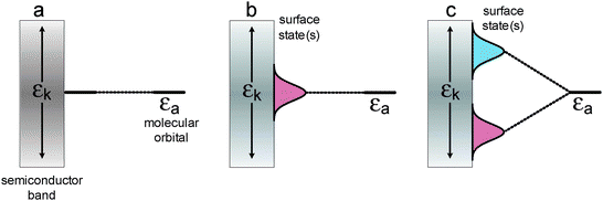 | ||
| Fig. 7 Energy diagrams for surface-modified semiconductors in the case of: no electronic coupling (a); weak electronic coupling (b) and strong electronic coupling (c). εk stands for an electronic continuum of the metal or semiconductor electronic band. | ||
3.2. Modification with organic molecules
The photoelectrochemical properties of wide-band-gap semiconductors have been applied in the construction of numerous photoelectrochemical logic gates operating at the nanoscale. Photoelectrochemical photocurrent switching constitutes the basis for many of the semiconductor-based photoelectrochemical logic gates. Surface modification of wide-band-gap semiconductors with redox-active species results in new materials exhibiting photoelectrochemical photocurrent switching phenomena. It was observed for titanium dioxide modified with inter aliacarotene,103thiamine,92folic acid76 and carminic acid.104 Photoelectrodes built from those materials generate photocurrent, the polarity of which depends on photoelectrode potential, and/or the wavelength of incident light.One of the most famous molecular electronic devices is the molecular rectifier based on the D–σ–A molecular framework. The first molecular rectifier was theoretically predicted in 1974 by Aviram and Ratner, who suggested a model consisting of a donor π-system and an acceptor π-system, separated by a σ-bonded tunneling bridge. Molecules comprised of an electron donor and electron acceptor with delocalized π-electron systems linked with an aliphatic bridge are of potential interest for molecular and organic electronics.28,30,31,105,106Folic acid (FA) (Chart 1) is one of the redox active chromophores. Its structure is analogous to that of the Aviram–Ratner “Gedankenmolekül” (vide supra). It is an example of a molecular D–σ–A system. Characteristic photocurrent generation of irradiated photoelectrodes prepared from FA@TiO2 is quite different from that recorded for neat titanium dioxide.76,107 In air-equilibrated and oxygen-saturated solutions at a positive polarization, the photoelectrode generates anodic photocurrents only (Fig. 8a). Reversal of the photocurrent direction is observed at negative polarization of the photoelectrode. In the visible part of the spectrum (300–550 nm) cathodic and anodic photocurrents are observed. In the absence of oxygen the photosensitization is moderate (up to 550 nm, Fig. 8b). At 200 mV only weak anodic photocurrents upon UV illumination are observed, so the material behaves like neat titanium dioxide. The mechanism of photocurrent switching can be ascribed by the photoinduced electron transfer involving both the folic acid molecule and the titanium dioxide support. Folic acid can donate or accept electrons if necessary so it operates as an electron buffer (Fig. 9). The direction of the photocurrent does not depend on the incident light wavelength, contrary to other switchable photoelectrochemical systems. Analogous photoactive materials were obtained by the chemisorption of carminic acid (CA) (Chart 2) onto nanocrystalline titanium dioxide.104Per analogiam to salicylic acid, strong electronic coupling was expected in this system which, however, does not provide any strong electronic coupling between the organic chromophore and titanium dioxide due to a very strong intramolecular coupling within the aromatic framework.
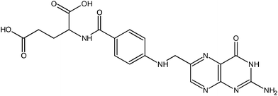 | ||
| Chart 1 Molecular structure of folic acid. | ||
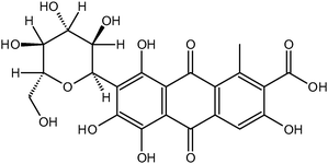 | ||
| Chart 2 Molecular structure of carminic acid. | ||
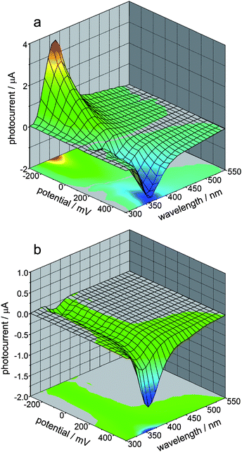 | ||
| Fig. 8 Photocurrent action spectra recorded at FA@TiO2 photoelectrodes as a function of electrode potential in oxygen-saturated (a) and deoxygenated (b) solutions. Adapted from ref. 76. | ||
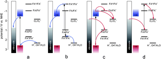 | ||
| Fig. 9 The mechanism of photocurrent generation (the PEPS effect): anodic photocurrent is generated at positive potentials upon excitation of the inner part of a TiO2 particle (a) and surface folic acid (b), while cathodic photocurrents are generated at negative potentials upon excitation of TiO2 (c) or folic acid (d). Shaded vertical bar indicates the photoelectrode potential. Adapted from ref. 76. | ||
Thiamine is another interesting redox-active biomolecule but it cannot be chemisorbed directly onto to the surface of titanium dioxide – it requires a suitable anchoring group. It is well known that TiO2 shows a strong tendency to bind various cyanoferrate complexes that allow photocurrent switching (penta- and hexacyanoferrates). Titanium dioxide is efficiently photosensitized by the pentacyanoferrate(II) complex with thiamine as the sixth ligand. The complex is easily bound to the TiO2 surface via an axial cyanide bridge. The electronic structure of the surface complex allows a facile electron transfer from the FeII center to the conduction band of the semiconducting electrode. The potential window for photosensitization might be extended by use of thiamine as the sixth ligand as compared to hexacyanoferrate (vide infra) and other pentacyanoferrates.91 Switching between anodic and cathodic photocurrents can be caused by varying the photoelectrode potential or the wavelength of the incident light. The photoelectrochemical photocurrent switching and redox-tuning photosensitization effect offers a possibility for constructing novel optoelectronic devices.92
Another device is based on photovoltaic responses observed during irradiation of an ITO electrode spin-coated with a mixture of TiO2 nanoparticles, polyvinylcarbazole, and carotenoid (Chart 3).103 Thus-prepared photoelectrodes were immersed in an aqueous KCl solution also containing hydroquinone (QH2) as a sacrificial electron donor. The anodic photocurrent involved electron transfer from the excited state of the carotenoid to the TiO2 conduction band; the resulting carotenoidradical cation is reduced by QH2. In contrast, when the aqueous electrolyte solution was saturated with O2, a cathodic photocurrent was observed; this reversal of polarity is attributed to electron transfer from the excited state of the carotenoid to O2, and subsequent reduction of the resulting carotenoid by electrons from the TiO2 conduction band.
 | ||
| Chart 3 Molecular structure of 7′-apo-7′-(4-carboxyphenyl)-β-carotene. | ||
All of these materials generate photocurrents on irradiation at 300–550 nm, but the photocurrent direction depends on the photoelectrode potential. Anodic photocurrents are observed at potentials higher than the switching point, while at lower potentials the electrodes generate cathodic photocurrents. One can ascribe the logic values of “0” to the negative and “1” to the positive polarization of the photoelectrode. The switching characteristics of these photoelectrodes allow them to be used as optoelectronic two-channel demultiplexers. The demultiplexer is a combinatorial logic device that takes data from a single input and directs it into a selected output. The addressing input determines to which data output the input pulse is directed, while all the other data outputs will get the value “0”. The simplest demultiplexer can be built from two AND gates and one NOT gate (Fig. 10). Photoelectrodes fabricated from surface-engineered wide-band-gap semiconductors can be also regarded as demultiplexers. In this case the device accepts information bits in the form of light pulses, while the photoelectrode polarity is regarded as an addressing input. Depending on the photoelectrode polarity, anodic or cathodic photocurrent pulses are generated, which in turn can be regarded as information bits directed into two distinct output channels (Table 1, Fig. 10).
| Light | Input 1 | Photoelectrode potential | Input 2 | Photocurrent | Output 1 | Output 2 |
|---|---|---|---|---|---|---|
| OFF | 0 | positive | 0 | NO | 0 | 0 |
| ON | 1 | positive | 0 | cathodic | 1 | 0 |
| OFF | 0 | negative | 1 | NO | 0 | 1 |
| ON | 1 | negative | 1 | anodic | 0 | 0 |
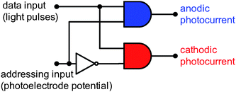 | ||
| Fig. 10 Electronic-equivalent circuit of a surface-modified titania photoelectrode working as a two-channel optoelectronic demultiplexer. Adapted from ref. 76. | ||
Bard has studied spectral sensitization by metal-free phthalocyanine (H2Pc) films on various semiconductor electrodes (single crystal n-TiO2, n-SrTiO3, n-WO3, n-ZnO, n-CdS, n-CdSe, n-Si, and n-GaP; at SnO2 conducting glass).108 The spectral response of the sensitized photocurrent was generally the same as the absorption spectrum of phthalocyanine. The composite photoelectrodes generated both anodic and cathodic photocurrents depending on the applied potential. The anodic photocurrents represented the usual sensitization of n-type semiconductors, while the cathodic photocurrents were attributed to the p-type behavior of the phthalocyanine itself. The current–potential curves of the semiconductor electrodes depended on the nature of the H2Pc films, the presence of a redox couple (i.e., p-hydroquinone/p-benzoquinone) in solution and the wavelength of incident light.
The behavior of photoelectrochemical cells composed of SnO2 or Pt electrodes coated with various phthalocyanines (H2Pc, ZnPc, MgPc, CuPc, InPc) were investigated by Bard et al.109 In these systems spectral sensitization at the SnO2/Pc interface leads to photooxidation currents, while efficient photoreduction occurs at the Pc/solution interface through bulk generation of charge carriers. The presence of both anodic and cathodic photocurrents leads to different net photocurrent responses for back- and front-side illumination, especially with thicker films. The nanoscale version of analogous switching devices, based on nickel–silicon nanowire Schottky junctions, is described in Section 4 (vide infra).
Another switching system that would have potential applications in photovoltaic conversion research as well as artificial smart materials is a system designed by the immobilization of CdSe/ZnS core–shell QDs and functionalized i-motif motor DNA on the surface of a gold electrode.110 Jiang’s group designed a highly reversible pH-driven photoelectric conversion switch by combining the broad absorption of CdSe/ZnS core–shell QDs and the pH-sensitive conformation of i-motif motor DNA, which referred to a broad-absorption light center and adjustable distance of the electron transport route (Fig. 11). Through tuning the pH value, the changeable conformation of motor DNA would alter the distance between CdSe/ZnSQDs and the Au electrode, so that a dynamic photoelectric conversion system could be achieved.
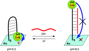 | ||
| Fig. 11 Scheme of the QDs–motor DNA–Au conjugate electrode. The electron-transfer process from photoexcited QDs to the Au electrode is modulated by the motor DNA's conformation change which is driven by changing the pH value of the electrolyte. Adapted from ref. 110. | ||
Willner and his group demonstrated the use of an electrode covered with CdSnanoparticles assembled with double-stranded deoxyribonucleic acid (dsDNA)111 for potential- and/or intercalator-induced photocurrent switching. The photocurrent generated by the CdSnanoparticle/dsDNA with the use of the intercalators (polycyclic aromatic molecules) corresponds to an AND logic gate in which photocurrent is generated only if the optical signal and intercalator are applied as activation stimului to the system. The potential-controlled generation of the photocurrent in the system allows the direction of the output photocurrent in the presence of a sacrificial electron donor (triethanolamine) or acceptor (molecular oxygen). Operation of the switching device is based on the interplay between the electron donor/acceptor character of the electrolyte and photoelectrode polarization (photocurrent polarity) while DNA–intercalator binding controls the electrical conductivity of dsDNA.
The same principle of conductivity control at the nanoscale was reported for another switchable system based on CdSnanoparticles incorporated into a poly(acrylic acid) (PAA) film deposited on a gold electrode (Fig. 12).112 The nanoparticles are covalently linked to the matrix. Cu2+ ions are incorporated into the CdS–nanoparticle–PAA film, and the electroswitchable photocurrent generation by the system, in the presence of triethanolamine as a sacrificial electron donor, was demonstrated. The electrochemical reduction of the CdS–Cu2+–PAA state to the CdS–Cu0–PAA state leads to the formation of conductive metal nanoclusters that facilitate transfer of the CdS–conduction-band electrons to the electrode, and the generation of the photocurrent. Oxidation of the Cu0 clusters to Cu2+ ions linked to the carboxylate units of PAA switches off the photocurrent. The system is active not only for reversible electroswitchable photocurrent generation but also acts as a photoelectrochemical detector of Cu2+ ions.
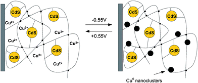 | ||
| Fig. 12 Electrochemical switching of the CdS–polymer film between the CdS–Cu2+–PAA and CdS–Cu0–PAA states. Adapted from ref. 112. | ||
3.3. Modification with transition metal complexes
The photoelectrochemical photocurrent switching effects described above are based on photoinduced electron-transfer processes between band or surface states of semiconductor and electronic levels of adsorbed molecules (Fig. 13). While excitation of oxidized surface species results exclusive in anodic photocurrents (Fig. 13b), upon reduction, cathodic photocurrents can be observed both on excitation of surface states (Fig. 13c) and fundamental transitions (Fig. 13d). Operation of this mechanism requires appropriate redox properties of the chemisorbed species – it should undergo reversible oxidation/reduction processes both in its ground (electrochemical charge transfer) and excited states (photoinduced charge transfer). Coordination compounds of transition metal ions usually offer a number of stable oxidation states in a broad range of potentials. Moreover, inorganic or organic ligands may facilitate covalent bonding to the surface of the semiconducting nanoparticle. This feature may play a crucial role in the photocurrent generation since the electronic coupling between the formed surface complex and the support should enhance the rate and efficiency of the interfacial charge transfer. | ||
| Fig. 13 The simplified mechanism of photocurrent generation at neat TiO2 photoelectrodes (a), TiO2electrode with oxidized surface complex (b) and reduced surface complex (c, d). Adapted from ref. 79. | ||
A good example of a coordination compound/semiconductor system capable of photocurrent switching is [Fe(CN)6]3−/4−@TiO2. Chemisorption of the hexacyanoferrate anion is realized through the axial cyanide bridge linking titanium with iron ions.90 The photoelectrochemical behavior of this system is demonstrated in Fig. 14.77 The photosensitization to visible light occurs only at potentials lower than ca. 200 mV, i.e. when the reduced form of the complex prevails. Under these conditions, excitation with visible light within the MMCT (metal-to-metal charge transfer) or MPCT (metal-to-particle charge transfer) results in direct electron transition between FeII and TiIV according to the Creutz, Brunschwig, and Sutin model.100 The fate of an electron from the conduction band depends on the presence of an acceptor moiety – in the presence of oxygen, electrons reduce O2 to the superoxide anion while the oxidized form of hexacyanoferrate is reduced back to the original oxidation state II. Cathodic photocurrents evolve independently if UV or visible light is applied (Fig. 13). Anodic photocurrents can be recorded when the oxidized hexacyanoferrate prevails (at potentials higher than 200 mV; Fig. 13) – under these conditions an electron transfer from the conduction band to the electrode can be observed together with the oxidation of sacrificial reagents (e.g.water or other donor molecule) by valence band holes.
![Photocurrent response of the photoelectrode covered with [Fe(CN)6]3−/4−@TiO2. Adapted from ref. 77.](/image/article/2009/NR/b9nr00145j/b9nr00145j-f14.gif) | ||
| Fig. 14 Photocurrent response of the photoelectrode covered with [Fe(CN)6]3−/4−@TiO2. Adapted from ref. 77. | ||
Due to variable photocurrent responses of the [Fe(CN)6]3−/4−@TiO2 system depending on both the applied potential and color of the incident light, the photoelectrode covered with this material may constitute a good platform for construction of the XOR gate.78,80 Application of UV (or violet) and blue light sources (for instance LEDs, Fig. 15) results in the generation of positive, negative or null photocurrents, depending on the electrode potential and the state of the light source (on-off). At electrode potentials ensuring a complete oxidation of the surface complex (e.g. +400 mV vs.Ag/AgCl) irradiation with violet light (λmax = 400 nm) generates anodic photocurrents. Since no photosensitization takes place at these potentials, irradiation with blue light does not induce any current. When the iron complex is reduced (e.g. −200 mV vs.Ag/AgCl) irradiation with either violet or blue light generates cathodic photocurrent; its amplitude depends on the total light intensity. Considering two light sources as input channels in the states “0” or “1” when the diodes are off or on, respectively, and the photocurrent as an output channel (“0” corresponds to null net photocurrent and “1” to any non-zero photocurrent), the presented two regimes of work correspond to the YES and OR functions (Fig. 15). The most interesting behavior of the system can be observed at the potential of ca. 250 mV, i.e. under conditions of partial reduction of the surface complex. Illumination with the violet LED generates anodic photocurrents while application of blue light induces cathodic photocurrents. Bichromatic irradiation gives a net null photocurrent, despite sharp short signals which appear immediately upon switching on or off the LEDs (Fig. 15). This behavior describes the XOR logic function which yields low output (logical 0) when both inputs are equal and “1” and high output (logical 1) when inputs are different. The described system constituted the first example of a photochemical XOR logic gate with two optical inputs. Moreover, the programmable (by applied potential) character of the device makes the system very versatile (Fig. 15).
![Electronic equivalent circuit for a programmable logic system based on a [Fe(CN)6]3−/4−@TiO2-covered electrode: depending on the potential the system performs OR, XOR or YES functions. Recorded photocurrents (right) correspond to pulsed irradiation with violet (400 nm) and blue (460 nm) LEDs (left). Adapted from ref. 80.](/image/article/2009/NR/b9nr00145j/b9nr00145j-f15.gif) | ||
| Fig. 15 Electronic equivalent circuit for a programmable logic system based on a [Fe(CN)6]3−/4−@TiO2-covered electrode: depending on the potential the system performs OR, XOR or YES functions. Recorded photocurrents (right) correspond to pulsed irradiation with violet (400 nm) and blue (460 nm) LEDs (left). Adapted from ref. 80. | ||
The described [Fe(CN)6]3−/4−@TiO2 system can be tuned by changing two basic factors: redox potential of the surface complex and the strength of the complex–support electronic interaction. The redox potential of the FeIII/FeII couple and therefore the switching potential depends on the coordination sphere of the iron ion. It has been demonstrated that the series of pentacyanoferrate complexes with ammonia or thioethers as the sixth ligand offers a switching potential range of 240 to 410 mV vs.Ag/AgCl. The variation of the switching potential with the ligand structure can be ascribed to electronic effects of substituents.91,92
The second possibility of influencing the photocurrent response of the FeIII/II@TiO2 system is based on the changes in binding modes of the iron complex.77Hexacyanoferrate chemisorbed at the TiO2 surface and physisorbed ferrocene are on two opposite sides of the series describing the strength of the complex–support electronic coupling. Ferrocenylboronic acid chemisorbed at TiO2 due to a boronic group interaction with the surface hydroxyl groups or titanium(IV) centers presents a transient situation – although the complex undergoes a chemisorption process, the boronic moiety between iron and titanium centers prevents an efficient electron exchange due to the lack of π-orbitals. With decreasing efficiency of the modifier–semiconductor interaction, the photosensitization of titanium dioxide to visible light weakens, and photocurrent switching realized by the incident light wavelength becomes practically impossible. The behavior of a photoelectrode covered with ferrocene@TiO2 resembles that of a composite Prussian blue/TiO2 composite (vide infra).
The photocurrent switching phenomenon was also observed for titanium dioxide modified with nickel and indium hexacyanoferrates.113,114 Recently the PEPS effect was also observed in the case of photoelectrodes covered with TiO2 modified by chromium(VI) moieties (chromates and fluorochromates; unpublished data).
Presented coordination compound-based systems operate upon an electron excitation from a modifier to the conduction band of a semiconducting support. Due to photosensitization, cathodic photocurrents may be generated. Alternatively, prospective systems might operate upon hole-injection from a modifier to the valence band of a semiconductor – this type of photosensitization should result in anodic photocurrent evolution. Although the simplest Boolean operations performed by such systems should resemble those already described, the composite of these two types of particles might enable simulation of even more complex electronic circuits.
4. Composite semiconducting materials
4.1. Bulk doping and surface-state induced switching
The simplest material in which photoelectrochemical photocurrent switching is observed is selenium. Photoelectrochemical investigation on a trigonal selenium film shows the unusual n-type photocurrent generation. Selenium is a p-type semiconductor with a band gap energy of 1.9 eV and only cathodic photocurrents should be observed.115 Similar switching phenomena were observed in other p-type semiconductors like CdTe116 and CdSe.117 Photocurrent switching was also observed in the n-type semiconductor – CdS.118–121 In all these cases the photocurrent switching effect is associated with additional energy levels within the band gap. This phenomenon is associated with structure defects, surface contaminations or bulk doping. For example, the photoelectrochemical behavior of photoelectrodes prepared from sulfur-doped CdS nanopowder is dramatically different from the behaviour of neat (i.e. undoped) CdS. In the second case only anodic photocurrents were observed which was in accordance with predictions. Furthermore, the photocurrent intensity decreased as the photoelectrode potential became negative and approached the pseudo-Fermi level of CdS. A similar effect was noticed in S-doped cadmium sulfide, but in this case, negative polarization of the photoelectrode results in the generation of cathodic photocurrents. At the potentials close to the switching point, variation in the incident light wavelength also results in photocurrent switching (Fig. 16b). This indicates that the sulfur-centered traps (and other electronic levels associated with the so-called ‘Urbach tail’)121–124 are involved in the direction of electron transfer (Fig. 16a). When high-energy excitation was used, electrons were transferred to the conduction band and only anodic photocurrents were observed. In the case of low-energy excitation, electrons were trapped at a level associated with interstitial sulfur atoms (0.2–0.4 eV below the conduction band edge). Trapped electrons cannot be transferred to the conducting band and reduction of an electron acceptor present in the solution is observed as a cathodic photocurrent (Fig. 16c). These interesting photoelectrochemical properties of S-doped CdS should allow construction of optoelectronic logic devices. | ||
| Fig. 16 Diffuse reflectance spectra with characteristic Urbach tails (a), photocurrent action spectrum at the switching potential (b) and the mechanism of the switching process (c) S-doped CdS. αKM – Kubelka–Munk function. | ||
In the case of selenium, the normal cathodic photocurrent is caused by the photocorrosion process that in Se consists of two steps (4) and (5).115
| Se + H+ + e− → HSe | (4) |
| HSe + H+ + e− → H2Se | (5) |
The last step of photocorrosion can be prevented if suitable redox reaction can compete with it (eqn (6)).
| HSe + ox → Se + H+ + ox− | (6) |
An unusual anodic photocurrent is observed only upon anodic polarization when the electrode potential is lower than the Fermi potential of the semiconductor. It means that anodic photocurrent is associated with photocatalytic oxidation of a product of the cathodic photocorrosion. The energy levels of the intermediate states are located within the band gap and the direction of electron transfer is associated with surface states. The selenium photoelectrode is not suitable for building a regenerative solar cell, due to the fact that stabilization can be reached only with redox couples, but it might be used in a novel way for hydrogen production.
The photocurrent switching effect has also been observed in some semiconductor quantum dots: q-PbS125 and q-CdS.126 Contrary to the bulk semiconductor, in the case of quantum dots photocurrent switching operates according to a different mechanism. In bulk semiconductors the fate of the photogenerated electrons and holes is determined by the electric field at the interface (band bending) in the space-charge region: in the absence of specific doping or surface modification n-type semiconductors generate anodic photocurrents, while p-type semiconductors generate cathodic ones. In the case of quantum dots the band bending does not exist and photogenerated charge carriers are predicted to extend to the surface and engage in competition between recombination, photooxidation and photoreduction processes. Therefore the photocurrent direction in quantum dots depends mainly on redox agents present in the electrolyte and/or the applied potential.125,126
Bidirectional photocurrent flow in q-PbS can be associated with the presence of electron donor or acceptor surface states. At high photoelectrode potential, photoexcitation leads to electron trapping in empty surface states and cathodic photocurrents are observed (Fig. 17a). At negative polarization PbSquantum dots become partially reduced and the character of the surface states changes from electron acceptor to electron donor. Therefore photoexcitation results in electron transfer from the partially occupied surface states to the valence band and anodic photocurrents are observed (Fig. 17b). These phenomena are similar to the dynamic doping observed in memristive MIM devices (vide supra). Furthermore, photocurrent switching processes at q-PbSelectrodes can be observed in the presence of electron donors or electron acceptors in the electrolyte solution. In the presence of benzoquinone as an electron scavenger only cathodic photocurrents at negative potentials (−0.3 V) can be recorded. This observation can be explained by the photoreduction of benzoquinone by photogenerated electrons trapped at surface states. The opposite behavior was found in the presence of methyl viologen as a hole scavenger in the solution – the anodic photocurrent was recorded as a result of MV•+ photooxidation. Another interesting result was obtained under q-PbS illumination in a solution containing sulfide and polysulfide – both anodic and cathodic photocurrents were observed depending on the bias potential. At negative potentials (−0.5 V) the photoassisted reduction of S2−2 to S2− took place, and only cathodic photocurrents were observed. At slightly higher potentials (−0.4 V) photooxidation of S2−2 to elemental sulfur resulted in anodic photocurrents.125
 | ||
| Fig. 17 Scheme showing the predominant charge-transfer processes related to photoelectrochemical photocurrent switching of quantum dot photoelectrodes: PbS (a,b) and (PDDA/q-CdS)n (c, d). White and yellow Gaussian envelopes denote empty and occupied surface states, respectively. Adapted from refs. 125 and 126. | ||
A similar effect was described by Halaoui and co-workers in detail.126 The authors studied multilayers of polyacrylate-capped CdSquantum dots (q-CdS) embedded in poly(diallydimethylammonium chloride) (PDDA) with an alkaline sulfide solution interface. Depending on the bias potential, cathodic or anodic photocurrents were observed. At a potential of −0.2 V anodic photocurrents were observed (Fig. 17c) as a result of electron transfer to the electrode (processes 4a, 4b) competing with electron trapping at the surface states (2a). At the same time, photogenerated holes are scavenged by S2− (3a, 3b). Photocurrent direction was changed when the potential became more negative (−0.5 V) (Fig. 17d) and then holes are transferred to the electrode while the sulfide anions are oxidized. Photogenerated electrons are trapped in surface states (SS) and/or photocatalyze hydrogen evolution (2a, 5a, 5b).126
4.2. p–n bulk heterojunctions
The photoelectrochemical photocurrent switching effect was observed in the case of some materials of a p–n bulk heterojunction character.127–135 A p–n bulk heterojunction is a semiconductor composite consisting of two mixed semiconductor powders (n- and p-type) or semiconductor crystallites immersed in a semiconducting matrix of the opposite doping type. Generally the switching behavior in this class of semiconductor materials can be observed if two main criteria are fulfilled: optical and electrical. The optical criterion ensures different band-gap energies of n- and p-type components, while the electrical one involves appropriate band edge positions in both components in order to facilitate electron transfer.First of all, neat n- or p-type semiconductors upon band gap excitation can generate only anodic or cathodic photocurrents, respectively. It is associated with their conductivity type – anodic photocurrent is characteristic for n-type semiconductors whereas cathodic photocurrent is characteristic for p-type semiconductors.136 Secondly, semiconductors within heterojunction materials must have different values of band gap energies – one of them should have a smaller band gap than the other (Fig. 18). During irradiation by high-energy light the cathodic and anodic photocurrents for both semiconductors are observed (red and blue lines in Fig. 18b). When lower energy light is used, only photocurrent characteristics for the semiconductor with the lower band gap can be observed. Finally, suitable band-edge potentials for semiconductors are necessary. Valence and conduction band positions in both semiconductors should be different. It is preferred that the potential of the conduction band edge in the semiconductor with the lower band gap should be lower. Such a situation enables the electron transfer from the conduction band of the lower band gap semiconductor to the conduction band of the semiconductor with a higher band gap (cf.Fig. 18b).
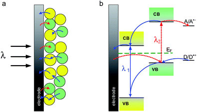 | ||
| Fig. 18 Diagram illustrating the direction of electron transfer at the p–n composite semiconductor photoelectrode (a) and the mechanism of cathodic (red line) and anodic (blue line) photocurrent generation at p–n bulk heterojunction (b). | ||
The interesting photoelectrochemical behavior was observed in the case of the M/TiO2 Schottky junction composites (where M = Se,129,130 Pt131). Photoelectrochemical measurements of photoelectrodes made of a Pt/TiO2 nanocomposite showed completely different results compared to those of pure TiO2. Under anodic polarization anodic photocurrents were observed at potentials above 0.2 V. Cathodic photocurrents were also observed in the case of a Pt/TiO2 nanocomposite at potentials below 0.2 V. Cathodic photocurrent intensity increased in oxygen-saturated electrolyte solutions, indicating that cathodic photocurrents can be ascribed to the reduction of oxygen by conduction-band electrons. At the interface between the metal and semiconductor a Schottky barrier is formed. The barrier value of the Pt/TiO2 interface is estimated from the work function of Pt (5.64 eV) and the electron affinity of TiO2 (4.0 eV) to be 1.64 eV. Electron transfer from Pt to TiO2 is possible only under irradiation with light of energy exceeding 1.64 eV. It should be noted that anodic photocurrents in the wavelength range from 450 to 750 nm were clearly observed for the Pt/TiO2 composite electrodes. The photon energy range of the nanocomposite is smaller than the band gap of TiO2 (3.2 eV, matching light absorption below 400 nm), indicating the existence of some energy levels in the optical band gap of TiO2 that contributes to the photoelectric response in visible light.131 In the case of Se/TiO2 the photocathodic effect was associated with the photoreduction of Se (to Se2−).129,137 After photogeneration of electron–hole pairs in Se at a negative potential (−0.4 V) the electrons are moved to the solution interface and are involved in the photoreduction of Se thus generating cathodic photocurrents. In the case of more positive potentials, anodic photocurrents are observed as a result of photogenerated hole-injection into the TiO2 valence band where they can participate in the oxidation of water molecules or surface hydroxyl groups.129
The photocurrent switching effect may be caused not only by changing the photoelectrode polarization but also by changing the wavelength of the incident light. The wavelength-controlled optoelectronic switch can be produced by assembling two simple semiconductor materials on an ITO conducting support (Fig. 18a).127,128 This phenomenon was observed in the case of n-TiO2-N/p-CuI,128n-BiVO4/p-Co3O4,134n-BiVO4/p-CuO134 and n-CdS/p-CdTe116 heterojunction composites. Depending on the wavelength of the incident light, anodic or cathodic photocurrents can be observed, as both components are excited with high-energy light, whereas low-energy light excites only a small band gap component. Because both n- and p-type materials (of different band gaps) are present at the photoelectrode, the observed photocurrent at each wavelength will be determined by the competition between the photoresponses of these two materials.128,134 As an example, one can consider the n-BiVO4/p-CuO composite. At a constant potential, only an anodic photocurrent response of BiVO4 is observed which is characteristic for n-type semiconductors. This is due to the reaction of photogenerated holes with water, whereby photogenerated electrons are transferred into ITO. This anodic photocurrent vanishes at 500–530 nm, corresponding to 2.4 eV band gap of BiVO4.127 At longer wavelengths, only cathodic photocurrents are observed as expected for p-type semiconductor (CuO) with a band gap of 1.2 eV.134 A similar photoelectrochemical behavior was observed in previous cases. This kind of modification stabilizes the photocurrent, increases efficiency of its generation and leads to compartmentalization of interfacial reduction and oxidation at the n-type component and the p-type component, respectively.
For n-CdS/p-CdTe solar cells, photocurrent switching is observed in two wavelength ranges. At short wavelengths, the induced negative photocurrent at forward bias can be interpreted as being a result of the modulation of a light-dependent barrier located in the front region of the device.138 At the very long wavelengths of about 1050–1100 nm in the range of the Urbach tail photocurrent switching was also observed (while the band gap of CdTe corresponds to 850 nm). In this case, anomalous anodic photocurrent is associated with defects in the CdTe structure supporting additional energy levels within the band gap.116 This effect corresponds to that observed in the case of S-doped CdS.121
A simple composite material formed from two inorganic components is made of titanium dioxide embedded in the Prussian blue matrix (TiO2–PB). Contrary to TiO2 modified with hexacyanoferrate complexes the electrodes covered with the TiO2–PB nanocomposites practically do not generate photocurrents upon visible light irradiation. The photoelectrochemical response is similar to that observed for Fc@TiO2 (vide supra) which in turn can also be regarded as a composite material. Since no photocurrent switching can be induced by color changes of the incident light, and the switching can be realized only by the potential change (around 0.2 V vs.Ag/AgCl) the system can serve as a simple two-channel demultiplexer, similar to CA@TiO2 and FA@TiO2 cases.
Another interesting group of materials which shows the photocurrent switching effect encompasses hybrid materials comprising organic p-type semiconductors and n-type inorganic semiconductors, such as polythiophene@TiO2122,124 or polybithiophene@TiO2121 core–shell composites. In such materials the photocurrent switching effect is associated with an appropriate polarization of the electrode and use of a suitable light wavelength. The photocurrent spectra measurements at various bias potentials showed very interesting switching effects. At positive polarization the cathodic photocurrent maximum at 530 nm was observed. This value corresponds to the optical absorption maximum of reduced polythiophene,139 whereas the anodic photocurrent peak observed at 320 nm corresponds to the excitation of the TiO2 core. An additional cathodic peak at 340 nm was observed but only at negative polarization (−0.3 V).135 This unexpected cathodic peak is associated with the changing surface state of TiO2-modified polythiophene.133,135 When polythiophene is immersed into an electrolyte, band bending appears. During illumination by light with energy higher than band gap energy the photogenerated holes move to the bulk of the semiconductor while electrons move to the surface. The cathodic photocurrent is a result of reduction taking place at the surface of the semiconductor.133 A similar photocurrent switching effect was observed in a polybithiophene@TiO2 composite.132 Depending on the value of the applied potential, anodic or cathodic photocurrents were observed. The band model explains this phenomenon in a simple way. Under anodic polarization (0 V) band bending is observed only for a p-type semiconductor (polybithiophene) and results in a cathodic photocurrent. At more positive potentials (∼0.5 V) a depletion layer exists in both materials thus anodic and cathodic photocurrents for both components were measured. With increasing potential, new energy levels were created in the band gap of polybithiophene. Oxidation of polybithiophene results in a partial depopulation of these levels. When the potentials reach the value of 1 V, polybithiophene is in the metallic-like state and only an anodic photocurrent for TiO2 is observed.132 Good mechanical properties and high stability of polybithiophene are very advantageous with respect to its use in photovoltaics. Recently, efforts have been made to develop all-solid-state titanium dioxide photocells. A combination of TiO2 and polythiophene was one of the possible concepts.
The potential of the abovementioned bulk heterojunction materials can be further developed by applying better control of composition and dimensionality of these systems and devices. The reliability of the optoelectronic switching devices based on stochastic mixtures of two kinds of semiconducting particles can be greatly improved by controlling the geometrical arrangement between individual components. Semiconducting heterointerfacial structures are among the most promising assemblies for future electronics and optoelectronics,140–142 they can serve as both light sources143 and light-operated devices.144
A very interesting example of photocurrent switching was reported by Ahn and co-workers in 2005.144 The device comprised a silicon nanowire deposited on SiO2-coated silicon wafer (gate) and two nickel contacts (source and drain). Focused illumination of any Ni–Si junction resulted in Schottky photocurrent generation (Fig. 19). The polarity of the generated photocurrent at zero bias depended on the illumination site, as due to Schottky barriers at the metal–semiconductor interface, photoexcited electrons were always injected into the closest metal contact. Therefore illumination of the source area resulted in anodic photocurrents, while illumination of the drain area in cathodic ones. Further development of such systems based on heterostructure nanowires is almost unlimited owing to a rapid development of synthesis, manipulation and characterization techniques.145–153
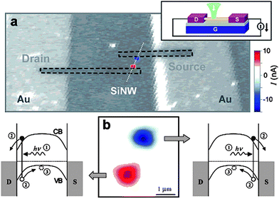 | ||
| Fig. 19 A scanning photocurrent image (color scale) overlaid on a confocal reflection image (grayscale) simultaneously taken at V = VG = 0 with a light intensity of 100 kW cm−2. The image size is 20 × 50 µm2. The direction of the positive current is indicated in the upper inset. Red (blue) corresponds to a positive (negative) current. In the reflection image, Ni electrodes (highlighted by dashed lines) are not visible because the light reflection from the Ni surface is weak at 532 nm (a). An enlarged photocurrent image from part (a) with energy-band diagrams describing the mechanism of the Schottky photocurrent generation (b). Reproduced from ref. 144 with permission. Copyright American Chemical Society 2005. | ||
5. Conclusions and outlook
Photoelectrochemical control over photocurrent generation in organic, inorganic and hybrid structures constitutes a universal platform for the construction of various switches, logic gates and more complex devices, including programmable logic gates and demultiplexers. The physical backgrounds of photocurrent switching phenomena are straightforward and simply involve thermodynamic competition between various pathways of photoinduced electron transfer. The chemical ways to control the photocurrent polarity are numerous and include selective excitation of designed chromophores/areas within nanostructures, redox processes involving surface dopants, fine tuning of interfacial electron-transfer energetics and other phenomena. Despite this apparent simplicity, the versatility of chemical systems in which these phenomena can be observed is overwhelming. The same response can be recorded for monomolecular layers of transition metal complexes and for bulk-doped nanocrystalline semiconductors and polymer–semiconductor composites. Furthermore, the combination of the plethora of photoswitchable systems with possible nanoscopic architectures may yield myriads of useful optoelectronic devices.While up to now, most of the molecular-scale logic devices have operated in solution and have used various chemical species as inputs, the PEPS-based optoelectronic devices use exclusively optical and electric input signals. This is the most important advantage of PEPS-based devices over any other molecular-scale logic devices, as the increase of complexity does not involve an increased number of different signaling molecules,23,154 but may only require an appropriate arrangement of individual switching devices, as was already achieved in the case of the neuron-like band microelectrode assemblies.155 Therefore semiconductor-based logic devices are good candidates to trade chemical complexity for geometrical complexity in order to increase computing power and performance of molecular-scale logic devices.156–158
The systems described above are unique among all computing devices. Due to their specific chemical structure they combine the unique features of electronic devices (communication in the electric domain) with the structural and functional versatility of molecules. Furthermore, as these systems can undergo chemical reactions and communicate with classical electronic devices, they constitute an ideal interface, which in the future should enable computing at the molecular scale. This is a great challenge as molecular-scale information processing is one of the most important missions of chemistry.15,159
Note added in proof
Very recently great progress was achieved in the field of molecular optoelectronic logic devices. The group of Tokuji Miyashita reported the very first solid-state two-electrode device.160 The device is based on ITO electrodes covered with Langmuir–Blodgett films of poly(N-dodecylacrylamide) covalently modified with ruthenium tris(bipyridine) (Ru) complex (acting as light harvesting antenna and electron acceptor) and ferrocene (Fc) moieties acting as electron donors. Photoelectrodes containing various sequences of donor and acceptor layers sandwiched the non-transparent gel electrolyte layer containing the sacrificial electron donor (triethanolamine) or sacrificial electron acceptor (bis(2-hydroxyethyl)viologen, HV2+). Depending on the sequence of the polymer layers, the OR (Fig. 20a) and XOR (Fig. 20b) logic gates were constructed. In the OR gate, illumination of any side of the device resulted in a low-intensity photocurrent, while concomitant illumination of both sides resulted in amplified photocurrent. Depending on the photocurrent threshold discriminating between logic 0 and logic 1 the same device can operate as the AND gate.Even simper device structure is required for the XOR gate. Illumination of any of the sides alone results in anodic or cathodic photocurrents, while in the case of simultaneous illumination of both sides of the device, the photocurrents compensate yielding null photocurrent response. This principle of operation is identical to that observed in other polymeric thin-layer devices and semiconducting devices based on the PEPS effect.
 | ||
| Fig. 20 Film structures and pathways of photoinduced electron transfer for OR (a) and XOR (b) gel photodiode logic devices. Adapted from ref. 160. | ||
Great progress was also reported in the case of nanowire-based optoelectronic switches (cf.Fig .19). A novel device reported by Lee et al.161 is based on carbon nanotube cross-junctions. Two single-walled carbon nanotubes of the same (metal–metal or semiconductor–semiconductor) or different (metal–semiconductor) conductivity type are crossed over a common gate thus forming a circuit of coupled nanotube field-effect transistors. Depending on the combination of nanotube conductivities and gate voltage various photocurrent patterns are observed: anodic or cathodic photocurrent are generated at nanotube terminals or at the cross-junction.
Even higher complexity of response was achieved when single-layered graphene, instead of nanowires, was used as a photoactive medium. A device contained a piece of single-layer graphene (12 μm long, 2.5 μm wide) with eight lithographically deposited gold–chromium electrodes, while the SiO2-covered silicon base acted as the back gate. Scanning photocurrent microscopy, combined with variation in electrode configurations resulted in very complex, two-dimensional photocurrent switching patterns. This is the very first example of optoelectronic integrated circuit based on a molecular material.162
Acknowledgements
This work was supported by the Polish Ministry of Science and Higher Education (grant No. 1609/B/H03/2009/36).References
- K. Szaciłowski, Chem. Rev., 2008, 108, 3481 CrossRef CAS.
- K. Szaciłowski, W. Macyk, A. Drzewiecka-Matuszek, M. Brindell and G. Stochel, Chem. Rev., 2005, 105, 2647 CrossRef CAS.
- M. P. Frank and T. F. Knight Jr., Nanotechnology, 1998, 9, 162 CrossRef.
- R. W. Keyes, Proc. IEEE, 2001, 89, 227 CrossRef CAS.
- J. D. Meindl, Q. Chen and J. A. Davis, Science, 2001, 293, 2044 CrossRef.
- V. A. Vashchenko and V. F. Sinkevitch, Physical limitations of semiconductor devices, Springer, New York, 2008 Search PubMed.
- J. D. Plummer and P. B. Griffin, Proc. IEEE, 2001, 89, 240 CrossRef CAS.
- D. Minolli, Nanotechnology Applications to Telecommunications and Networking, Wiley-Interscience, Hoboken, 2006 Search PubMed.
- J. M. Tour, Molecular electronics. Commercial Insights, Chemistry, Devices, Architecture and Programming, World Scientific, New Jersey, 2003 Search PubMed.
- Introducing molecular electronics, ed. G. Cuniberti, G. Fagas, K. Richter, Springer Verlag, Berlin, 2005 Search PubMed.
- Nanotechnology and nanoelectronics, ed. W. R. Fahrner, Springer Verlag, Berlin, 2005 Search PubMed.
- M. Dragoman and D. Dragoman, Nanoelectronics. Principles and devices, Artech House, Inc., Norwood, MA, 2006 Search PubMed.
- Nano and Molecular Electronics, ed. S. E. Lyshevski, CRC Press, London, 2007 Search PubMed.
- K. P. Zauner, Crit. Rev. Solid State Mat. Sci., 2005, 30, 33 Search PubMed.
- S. R. Hameroff, Ultimate computing. Biomolecular consciousness and nanotechnology, Elsevier Science, Amsterdam, 1987 Search PubMed.
- V. Balzani, A. Credi, and M. Venturi, Molecular devices and machines. Concepts and perspectives for the nanoworld, Wiley-VCH, Weinheim, 2008 Search PubMed.
- V. Balzani, A. Credi and M. Venturi, Chem.–Eur. J., 2008, 14, 26 CrossRef.
- A. P. de Silva, Y. Leydet, C. Lincheneau and N. D. McClenaghan, J. Phys.: Condens. Matter, 2006, 18, S1847 CrossRef.
- A. P. de Silva and N. D. McClenaghan, J. Am. Chem. Soc., 2000, 122, 3965 CrossRef CAS.
- A. P. de Silva and N. D. McClenaghan, Chem.–Eur. J., 2004, 10, 574 CrossRef.
- A. P. de Silva, S. Uchiyama, T. P. Vance and B. Wannalerse, Coord. Chem. Rev., 2007, 251, 1623 CrossRef.
- V. Balzani, A. Credi and M. Venturi, ChemPhysChem, 2008, 9, 202 CrossRef.
- J. Macdonald and Y. Li, Nano Lett., 2006, 6, 2598 CrossRef CAS.
- S. S. Li, Semiconductor physical electronics, Springer, New York, 2006 Search PubMed.
- The illustrated dictionary of electronics, ed. S. Gibilisco, McGraw-Hill, New York, 2001 Search PubMed.
- J. C. Ellenbogen and J. C. Love, Proc. IEEE, 2000, 88, 386 CrossRef CAS.
- A. Aviram and M. A. Ratner, Chem. Phys. Lett., 1974, 29, 277 CrossRef CAS.
- H. Meier, Angew. Chem., Int. Ed., 2005, 44, 2482 CrossRef CAS.
- R. M. Metzger, Chem. Rev., 2003, 103, 3803 CrossRef CAS.
- R. M. Metzger, Colloids Surf., A, 2006, 284–285, 2 CrossRef.
- M. Bendikov, F. Wudl and D. F. Perepichka, Chem. Rev., 2004, 104, 4891 CrossRef CAS.
- J. Shinar and R. Shinar, J. Phys. D: Appl. Phys., 2008, 41, 133001 CrossRef.
- J. Kido and Y. Okamoto, Chem. Rev., 2002, 102, 2357 CrossRef CAS.
- S. Günes, H. Neugebauer and N. S. Sariciftci, Chem. Rev., 2007, 107, 1324 CrossRef.
- Organic photovoltaics. Concepts and realization, ed. C. J. Brabec, V. Dyakonov, J. Parisi, N. S. Sariciftci, Springer Verlag, Berlin, 2003 Search PubMed.
- P. W. M. Blom, V. D. Mihailetchi, L. J. A. Koster and D. E. Markov, Adv. Mater., 2007, 19, 1551 CrossRef CAS.
- A. Wicklein, S. Ghosh, M. Sommer, F. Würthner and M. Thelakkat, ACS Nano, 2009, 3, 1107 CrossRef CAS.
- J.-L. Brédas, D. Beljonne, V. Coropceanu and J. Cornil, Chem. Rev., 2004, 104, 4971 CrossRef CAS.
- F. J. M. Hoeben, P. Jonkheijm, E. W. Meijer and A. P. H. J. Schenning, Chem. Rev., 2005, 105, 1491 CrossRef CAS.
- A. P. H. J. Schenning and E. W. Meijer, Chem. Commun., 2005, 3245 RSC.
- J. Wu, W. Pisula and K. Müllen, Chem. Rev., 2007, 107, 718 CrossRef CAS.
- K. Müllen and J. P. Rabe, Acc. Chem. Res., 2008, 41, 511 CrossRef.
- L. Zang, Y. Che and J. S. Moore, Acc. Chem. Res., 2008, 41, 1596 CrossRef CAS.
- M. D. Watson, A. Fechtenkötter and K. Müllen, Chem. Rev., 2001, 101, 1267 CrossRef CAS.
- J. C. Love, L. A. Estroff, J. K. Kriebel, R. G. Nuzzo and G. M. Whitesides, Chem. Rev., 2005, 105, 1103 CrossRef CAS.
- S. DiBenedetto, A. Fanchetti, M. A. Ratner and T. J. Marks, Adv. Mater., 2009, 21, 1407 CrossRef CAS.
- R. J. Forster and T. E. Keyes, Coord. Chem. Rev., 2009, 253, 1833 CrossRef CAS.
- V. Kriegisch and C. lambert, Top. Curr. Chem., 2005, 258, 257 CAS.
- P. F. H. Schwab, M. D. Levin and J. Michl, Chem. Rev., 1999, 99, 1863 CrossRef CAS.
- P. F. H. Schwab, J. R. Smith and J. Michl, Chem. Rev., 2005, 105, 1197 CrossRef CAS.
- N. Robertson and C. A. McGowan, Chem. Soc. Rev., 2003, 32, 96 RSC.
- D. K. James and J. M. Tour, Top. Curr. Chem., 2005, 257, 33 CAS.
- J.-W. Choi, G.-Y. Jung, S. Y. Oh, W. H. Lee and D. M. Shin, Thin Solid Films, 1996, 284–285, 876 CrossRef CAS.
- J.-C. Chambron, J.-P. Collin, J.-O. Dalbavie, C. O. Diederich-Buchecker, V. Heitz, F. Odobel, N. Soddadié and J.-P. Sauvage, Coord. Chem. Rev., 1998, 178–180, 1299 CrossRef CAS.
- J.-W. Choi, S. W. Chung, S. Y. Oh, W. H. Lee and D. M. Shin, Thin Solid Films, 1998, 327–329, 671 CrossRef CAS.
- J.-W. Choi, Y.-S. Nam, B.-S. Kong, H.-G. Choi, W. H. Lee and M. Fujihira, Colloids Surf., B, 2002, 23, 263 CrossRef CAS.
- J.-W. Choi, Y. S. Nam, S.-C. Jeong, W. H. Lee and M. C. Petty, Curr. Appl. Phys., 2006, 6, 839 CrossRef.
- J.-W. Choi, Y. S. Nam, S. Y. Oh, W. H. Lee and M. Fujihira, Mol. Cryst. Liq. Cryst., 2002, 377, 249 CrossRef CAS.
- J.-W. Choi, Y.-S. Nam and W. H. Lee, Mol. Cryst. Liq. Cryst., 2003, 407, 89 CrossRef.
- L. O. Chua, IEEE Trans. Circuit Theory, 1971, 18, 507 Search PubMed.
- D. B. Strukov, G. S. Snider, D. R. Stewart and R. S. Williams, Nature, 2008, 453, 80 CrossRef CAS.
- R. T. Weitz, A. Walter, R. Engl, R. Sezi and C. Dehm, Nano Lett., 2006, 6, 2810 CrossRef CAS.
- A. Sawa, Mater. Today, 2008, 11(6), 28 CrossRef CAS.
- S.-E. Ahn, M.-J. Lee, Y. Park, B. S. Kang, C. B. Lee, K. H. Kim, S. Seo, D.-S. Suh, D.-C. Kim, J. Hur, W. Xianyu, G. Stefanovich, H. Yin, I.-K. Yoo, J.-H. Lee, J.-B. Park, I.-G. Baek and B. H. Park, Adv. Mater., 2008, 20, 924 CrossRef CAS.
- R. Waser, R. Dittmann, G. Staikov and K. Szot, Adv. Mater., 2009, 21, 2632 CrossRef CAS.
- H. Choi, H. Jung, J. Lee, J. Yoon, J. Park, D.-J. Seong, W. Lee, M. Hasan, G.-Y. Jung and H. Hwang, Nanotechnology, 2009, 20, 345201 CrossRef.
- T. H. Kim, E. Y. Jang, N. J. Lee, D. J. Choi, K.-J. Lee, J.-t. Jang, J.-s. Choi, S. H. Moon and a. J. Cheon, Nano Lett., 2009, 9, 2229 CrossRef CAS.
- J. Matsui, M. Mitsuishi, A. Aoki and T. Miyashita, Angew. Chem., Int. Ed., 2003, 42, 2272 CrossRef CAS.
- J. Matsui, M. Mitsuishi, A. Aoki and T. Miyashita, J. Am. Chem. Soc., 2004, 126, 3708 CrossRef CAS.
- S. Yasutomi, T. Morita, Y. Imanishi and S. Kimura, Science, 2004, 304, 1944 CrossRef CAS.
- S. Yasutomi, T. Morita and S. Kimura, J. Am. Chem. Soc., 2005, 127, 14564 CrossRef CAS.
- H. S. Mandal, I. J. Burgess and H.-B. Kraatz, Chem. Commun., 2006, 4802 RSC.
- A. Sakamoto, Y. Matsuo, K. Matsuo and E. Nakamura, Chem.–Asian J., 2009, 4, 1208 CrossRef CAS.
- S. Nitahara, T. Akiyama, S. Inoue and S. Yamada, J. Phys. Chem. B, 2005, 109, 3944 CrossRef CAS.
- S. Nitahara, N. Tasaki, T. Akiyama and S. Yamada, Thin Solid Films, 2006, 499, 354 CrossRef CAS.
- S. Gawęda, G. Stochel and K. Szaciłowski, Chem.–Asian J., 2007, 2, 580 CrossRef CAS.
- W. Macyk, G. Stochel and K. Szaciłowski, Chem.–Eur. J., 2007, 13, 5676 CrossRef CAS.
- K. Szaciłowski and W. Macyk, Solid-State Electron., 2006, 50, 1649 CrossRef CAS.
- K. Szaciłowski and W. Macyk, Chimia, 2007, 61, 831 CrossRef CAS.
- K. Szaciłowski, W. Macyk and G. Stochel, J. Am. Chem. Soc., 2006, 128, 4550 CrossRef CAS.
- K. Szaciłowski, W. Macyk and G. Stochel, J. Mater. Chem., 2006, 16, 4603 RSC.
- M. Galperin and A. Nitzan, Phys. Rev. Lett., 2005, 95, 206802 CrossRef.
- M. Galperin, A. Nitzan and M. A. Ratner, Phys. Rev. Lett., 2006, 96, 166803 CrossRef.
- M. Galperin and A. Nitzan, J. Chem. Phys., 2006, 124, 234709 CrossRef.
- C. D. Lindstrom and X.-Y. Zhu, Chem. Rev., 2006, 106, 4281 CrossRef CAS.
- E. Vrachnou, M. Grätzel and A. J. McEvoy, J. Electroanal. Chem., 1989, 258, 193 CrossRef CAS.
- E. Vrachnou, N. Vlachopoulos and M. Grätzel, J. Chem. Soc., Chem. Commun., 1987, 868 RSC.
- H. N. Ghosh, J. B. Ashbury, Y. Weng and T. Lian, J. Phys. Chem. B, 1998, 102, 10208 CrossRef CAS.
- M. Khoudiakov, A. R. Parise and B. S. Brunschwig, J. Am. Chem. Soc., 2003, 125, 4637 CrossRef CAS.
- F. De Angelis, A. Tilocca and A. Selloni, J. Am. Chem. Soc., 2004, 126, 15024 CrossRef CAS.
- M. Hebda, G. Stochel, K. Szaciłowski and W. Macyk, J. Phys. Chem. B, 2006, 110, 15275 CrossRef CAS.
- K. Szaciłowski, W. Macyk, M. Hebda and G. Stochel, ChemPhysChem, 2006, 7, 2384 CrossRef CAS.
- J. A. Harris, K. Trotter and B. S. Brunschwig, J. Phys. Chem. B, 2007, 111, 6695 CrossRef CAS.
- C. Creutz and M. H. Chou, Inorg. Chem., 2008, 47, 3509 CrossRef CAS.
- L. G. C. Rego and V. S. Batista, J. Am. Chem. Soc., 2003, 125, 7989 CrossRef CAS.
- I. A. Janković, Z. V. Šaponjić, M. I. Čomor and J. M. Nedelković, J. Phys. Chem. C, 2009, 113, 12645 CrossRef CAS.
- T. Rajh, J. M. Nedeljkovic, L. X. Chen, O. Poluektov and M. C. Thurnauer, J. Phys. Chem. B, 1999, 103, 3515 CrossRef CAS.
- T. Sakata, K. Hashimoto and M. Hiramoto, J. Phys. Chem., 1990, 94, 3040 CrossRef CAS.
- O. Kitao, J. Phys. Chem. C, 2007, 111, 15889 CrossRef CAS.
- C. Creutz, B. S. Brunschwig and N. Sutin, J. Phys. Chem. B, 2005, 109, 10251 CrossRef CAS.
- C. Creutz, B. S. Brunschwig and N. Sutin, J. Phys. Chem. B, 2006, 110, 25181 CrossRef CAS.
- C. Creutz, B. S. Brunschwig and N. Sutin, Chem. Phys., 2006, 324, 244 CrossRef CAS.
- G. G. Gao, Y. Deng and L. D. Kispert, J. Chem. Soc., Perkin Trans. 2, 1999, 1225 RSC.
- S. Gawęda, G. Stochel and K. Szaciłowski, J. Phys. Chem. C, 2008, 112, 19131 CAS.
- R. M. Metzger, Acc. Chem. Res., 1999, 32, 950 CrossRef CAS.
- D. M. Guldi, G. M. A. Rahman, V. Sgobba and C. Ehli, Chem. Soc. Rev., 2006, 35, 471 RSC.
- K. Szaciłowski and W. Macyk, C. R. Chim., 2006, 9, 315 CrossRef CAS.
- C. D. Jaeger, F.-R. F. Fan and A. J. Bard, J. Am. Chem. Soc., 1980, 102, 2592 CrossRef CAS.
- P. Leempoel, F.-R. F. Fan and A. J. Bard, J. Phys. Chem., 1983, 87, 2948 CrossRef CAS.
- H. Meng, Y. Yang, Y. Chen, Y. Zhou, Y. Liu, X. Chen, H. Ma, Z. Tang, D. Liu and L. Jiang, Chem. Commun., 2009, 2293 RSC.
- R. Gill, F. Patolsky, E. Katz and I. Willner, Angew. Chem., Int. Ed., 2005, 44, 4554 CrossRef CAS.
- L. Sheeney-Haj-Ichia, Z. Cheglakov and I. Willner, J. Phys. Chem. B, 2004, 108, 11 CrossRef CAS.
- N. R. de Tacconi, K. Rajeshwar and R. O. Lezna, Electrochim. Acta, 2000, 45, 3403 CrossRef CAS.
- N. R. de Tacconi, K. Rajeshwar and R. O. Lezna, J. Electroanal. Chem., 2001, 500, 270 CrossRef CAS.
- W. Gissler, J. Electrochem. Soc., 1980, 127, 1713 CrossRef CAS.
- G. Agostinelli and E. D. Dunlop, Thin Solid Films, 2003, 431–432, 448 CrossRef CAS.
- P. Zhang, C. Cheng, P. Jiao, Y. Li, Z. He and H. Zhang, Mater. Lett., 2008, 62, 1151 CrossRef CAS.
- H. Minoura and M. Tsuiki, Chem. Lett., 1978, 205 CrossRef CAS.
- N. Müller, G. Hodes and B. Vainas, J. Electroanal. Chem., 1984, 172, 155 CrossRef.
- B. Vainas and G. Hodes, J. Electroanal. Chem., 1981, 130, 391 CAS.
- A. Podborska, B. Gaweł, Ł. Pietrzak, I. B. Szymańska, J. K. Jeszka, W. Łasocha and K. Szaciłowski, J. Phys. Chem. C, 2009, 113, 6774 CrossRef CAS.
- F. Urbach, Phys. Rev., 1953, 92, 1324 CrossRef CAS.
- A. E. Rakhshani, J. Phys.: Condens. Matter, 2000, 12, 4391 CrossRef CAS.
- M. Grus and A. Sikorska, Phys. B, 1999, 266, 139 CrossRef CAS.
- S. Ogawa, K. Hu, F. Fan and A. J. Bard, J. Phys. Chem. B, 1997, 101, 5707 CrossRef CAS.
- M. El Harakeh, L. Alawieh, S. Saouma and L. Halaoui, Phys. Chem. Chem. Phys., 2009, 11, 5962 RSC.
- M. Long, W. Cai and H. Kisch, J. Phys. Chem. C, 2008, 112, 548 CrossRef CAS.
- R. Beránek and H. Kisch, Angew. Chem., Int. Ed., 2008, 47, 1320 CrossRef CAS.
- S. Somasundaram, C. R. Chenthamarakshan, N. R. de Tacconi, Y. Ming and K. Rajeshwar, Chem. Mater., 2004, 16, 3846 CrossRef CAS.
- K. Rajeshwar, N. R. De Tacconi and C. R. Chenthamarakshan, Curr. Opin. Solid State Mater. Sci., 2004, 8, 173 CrossRef CAS.
- T. Sasaki, N. Koshizaki, J.-W. Yoon and K. M. Beck, J. Photochem. Photobiol., A, 2001, 145, 11 CrossRef CAS.
- U. Rammelt, N. Hebestreit, A. Fikus and W. Plieth, Electrochim. Acta, 2001, 46, 2363 CrossRef CAS.
- Q.-T. Vu, M. Pavlik, N. Hebestreit, U. Rammelt, W. Plieth and J. Pfleger, React. Funct. Polym., 2005, 65, 69 CrossRef CAS.
- M. Long, R. Beránek, W. Cai and H. Kisch, Electrochim. Acta, 2008, 53, 4621 CrossRef CAS.
- N. Hebestreit, J. Hofmann, U. Rammelt and W. Plieth, Electrochim. Acta, 2003, 48, 1779 CrossRef CAS.
- K. Rajeshwar, in Encyclopedia of electrochemistry, ed. A. J. Bard, M. Stratmann, S. Licht, Wiley-VCH, Weinheim, 2002, vol. 6, p. 1 Search PubMed.
- N. R. de Tacconi, C. R. Chenthamarakshan, K. Rajeshwar and E. J. Tacconi, J. Phys. Chem. B, 2005, 109, 11953 CrossRef CAS.
- G. Agostinelli, D. L. Bätzner and M. Burgelman, Thin Solid Films, 2003, 431–432, 407 CrossRef CAS.
- J. Pfleger, M. Pavlik, N. Hebestreit and W. Plieth, Macromol. Symp., 2004, 212, 539 CrossRef CAS.
- R. Agarwal, Small, 2008, 4, 1872 CrossRef CAS.
- C. Pan and J. Zhu, J. Mater. Chem., 2009, 19, 869 RSC.
- J. Hu, Y. Bando and D. Golberg, J. Mater. Chem., 2009, 19, 330 RSC.
- Y. Huang, X. Duan and C. M. Lieber, Small, 2005, 1, 142 CrossRef CAS.
- Y. Ahn, J. Dunning and J. Park, Nano Lett., 2005, 5, 1367 CrossRef CAS.
- Y. Xia, P. Yang, Y. Sun, Y. Wu, B. Mayers, B. Gates, Y. Yin, F. Kim and H. Yan, Adv. Mater., 2003, 15, 353 CrossRef CAS.
- C. N. R. Rao, F. L. Deepak, G. Gundiah and A. Govindaraj, Prog. Solid State Chem., 2003, 31, 5 CrossRef CAS.
- J. G. Lu, P. Chang and Z. Fan, Mater. Sci. Eng., R, 2006, 52, 49 CrossRef.
- S. V. N. T. Kuchibhatla, A. S. Karakoti, D. Bera and S. Seal, Prog. Mater. Sci., 2007, 52, 699 CrossRef CAS.
- Z. L. Wang, Adv. Mater., 2003, 15, 432 CrossRef CAS.
- X. Chen and S. S. Mao, Chem. Rev., 2007, 107, 2891 CrossRef CAS.
- G. K. Mor, O. K. Varghese, M. Paulose, K. Shankar and C. A. Grimes, Sol. Energy Mater. Sol. Cells, 2006, 90, 2011 CrossRef CAS.
- K. Shankar, J. I. Basham, N. K. Allam, O. K. Varghese, G. K. Mor, X. Feng, M. Paulose, J. A. Seabold, K.-S. Choi and C. A. Grimes, J. Phys. Chem. C, 2009, 113, 6327 CrossRef CAS.
- X. Fang, Y. Bando, U. K. Gautam, T. Zhai, S. Gradečak and D. Goldberg, J. Mater. Chem., 2009, 19, 5683 RSC.
- V. Privman, G. Strack, D. Solenov, M. Pita and E, Katz, J. Phys. Chem. B, 2008, 112, 11777 CrossRef CAS.
- C. Amatore, L. Thouin and J.-S. Warkocz, Chem.–Eur. J., 1999, 5, 456 CrossRef CAS.
- K. Szaciłowski, Chem.–Eur. J., 2004, 10, 2520 CrossRef.
- L. Lizana, Z. Konkoli and O. Orwar, J. Phys. Chem. B, 2007, 111, 6214 CrossRef CAS.
- O. Steinbock, P. Kettunen and K. Showalter, J. Phys. Chem., 1996, 100, 18970 CrossRef CAS.
- L. Piela, Ideas of Quantum Chemistry, Elsevier, Amsterdam, 2007 Search PubMed.
- J. Matsui, K. Abe, A. Aoki and T. Miyashita, Langmuir, 2009, 25, 11061 CrossRef CAS.
- E. J. H. Lee, K. Balasubramanian, M. Burghard and K. Kern, Adv. Mater., 2009, 21, 2720 CrossRef CAS.
- J. Park, Y. H. Ahn and C. Rioz-Vargas, Nano Lett., 2009, 9, 1742 CrossRef CAS.
| This journal is © The Royal Society of Chemistry 2009 |
