Enhanced Cu emission in ZnS![[hair space]](https://www.rsc.org/images/entities/h2_char_200a.gif) :Cu,Cl/ZnS core–shell nanocrystals
:Cu,Cl/ZnS core–shell nanocrystals
Carley
Corrado
a,
Morgan
Hawker
a,
Grant
Livingston
a,
Scott
Medling
b,
Frank
Bridges
b and
Jin Z.
Zhang
*a
aDepartment of Chemistry and Biochemistry, University of California, Santa Cruz, CA 95064, USA. E-mail: zhang@chemistry.ucsc.edu
bDepartment of Physics, University of California, Santa Cruz, CA 95064, USA
First published on 26th May 2010
Abstract
ZnS![[hair space]](https://www.rsc.org/images/entities/char_200a.gif) :Cu,Cl/ZnS core–shell nanocrystals (NCs) have been synthesized via a facile aqueous synthesis method. The shell growth of the NCs was observed via a red-shift in the UV-Vis absorption spectra with increasing NC size. The Cu photoluminescence (PL) emission was enhanced by capping with a thin ZnS shell. The ZnS:Cu (0.2%) and ZnS:Cu (0.5%) show a more pronounced red-shift in the apparent PL peak position as well as a 37% and 67% increase in emission intensity, respectively, in comparison to the undoped NCs. The observed red-shift is mainly due to an increase in intensity of the Cu PL emission. The 1% Cu-doped NCs exhibit very little red-shift because the observed emission is dominated by the Cu-dopant and thus nearly independent of the size of the NCs. The increase in Cu emission is evidence that Cu atoms occupying non-emissive surface sites in doped ZnS NCs were encapsulated by the ZnS shell. Extended X-Ray Absorption Fine Structure (EXAFS) data also suggests that the Cu had slightly more neighbors upon growth of a ZnS shell, indicating its encapsulation into the core of the NCs. The EXAFS Zn edge data also indicate greater disorder in the ZnS structure when the shell is grown, which may be attributed to the ZnS shell being more amorphous than the core NCs. This study demonstrates that core–shell structures can be used as a simple and yet powerful strategy to enhance PL properties of doped semiconductor NCs.
:Cu,Cl/ZnS core–shell nanocrystals (NCs) have been synthesized via a facile aqueous synthesis method. The shell growth of the NCs was observed via a red-shift in the UV-Vis absorption spectra with increasing NC size. The Cu photoluminescence (PL) emission was enhanced by capping with a thin ZnS shell. The ZnS:Cu (0.2%) and ZnS:Cu (0.5%) show a more pronounced red-shift in the apparent PL peak position as well as a 37% and 67% increase in emission intensity, respectively, in comparison to the undoped NCs. The observed red-shift is mainly due to an increase in intensity of the Cu PL emission. The 1% Cu-doped NCs exhibit very little red-shift because the observed emission is dominated by the Cu-dopant and thus nearly independent of the size of the NCs. The increase in Cu emission is evidence that Cu atoms occupying non-emissive surface sites in doped ZnS NCs were encapsulated by the ZnS shell. Extended X-Ray Absorption Fine Structure (EXAFS) data also suggests that the Cu had slightly more neighbors upon growth of a ZnS shell, indicating its encapsulation into the core of the NCs. The EXAFS Zn edge data also indicate greater disorder in the ZnS structure when the shell is grown, which may be attributed to the ZnS shell being more amorphous than the core NCs. This study demonstrates that core–shell structures can be used as a simple and yet powerful strategy to enhance PL properties of doped semiconductor NCs.
Introduction
Colloidal semiconductor nanocrystals (NCs) (also referred to as nanoparticles, NPs, or quantum dots, QDs) are of great interest and have been widely investigated due to their unique size and composition dependent properties.1–9 Doped NCs make up an important subgroup of nanomaterials where just a small percentage of an impurity or dopant is introduced to semiconductor NCs to alter their electronic, magnetic, and optical properties.10–17 One area of using doped semiconductor NCs is in AC Electroluminescence (EL) which is a promising technology for next-generation high efficiency solid-state lighting.12,18–22Cubic ZnS is a common and attractive choice as a host semiconductor for doping to produce nanophosphors in EL applications due to its stability, low cost, and low toxicity.12,20,22 A number of metal ions, such as Mn2+, Cu+, Pb2+, Ag+, and Eu2+, have been successfully doped into ZnS to produce PL or EL emission in different regions of the visible spectrum.23–29 In our previous work, photoluminescent ZnS:Cu NCs were synthesized via facile aqueous chemical precipitation method.30 Through EXAFS studies, it appeared that the Cu dopants were either on or near the surface of the NCs. In a related study, Mn in ZnSe![[thin space (1/6-em)]](https://www.rsc.org/images/entities/char_2009.gif) :Mn NCs has been found to be luminescent in core sites while non-luminescent in surface sites, suggesting that it is important to encapsulate the dopant ions into the core site.31 One possible strategy is to grow an undoped shell around doped core NCs. This has been demonstrated in the case of ZnS:Mn in which a ZnS shell grown around the Mn-doped ZnS core NCs was found to increase the PL intensity.32–34 Since MnS has the same cubic crystal structure and similar a-spacing as ZnS, 5.22 Å compared to 5.41 Å, respectively, the synthesis of ZnS:Mn/ZnS core–shell structure is relatively easy. CuS, the main precipitate in Cu-doped bulk ZnS,20 has a significantly different crystal structure than ZnS, and therefore Cu does not fit easily into the ZnS lattice. For Cu concentrations above ∼400–500 ppm, CuS-like precipitates form.35–37 Consequently, studies of Cu-doping are more challenging and for this reason, ZnS:Cu has not been investigated as widely as ZnS:Mn. The location of the Cu-dopant, particularly whether it is at or near the surface versus in the core of the NCs, is not understood.
:Mn NCs has been found to be luminescent in core sites while non-luminescent in surface sites, suggesting that it is important to encapsulate the dopant ions into the core site.31 One possible strategy is to grow an undoped shell around doped core NCs. This has been demonstrated in the case of ZnS:Mn in which a ZnS shell grown around the Mn-doped ZnS core NCs was found to increase the PL intensity.32–34 Since MnS has the same cubic crystal structure and similar a-spacing as ZnS, 5.22 Å compared to 5.41 Å, respectively, the synthesis of ZnS:Mn/ZnS core–shell structure is relatively easy. CuS, the main precipitate in Cu-doped bulk ZnS,20 has a significantly different crystal structure than ZnS, and therefore Cu does not fit easily into the ZnS lattice. For Cu concentrations above ∼400–500 ppm, CuS-like precipitates form.35–37 Consequently, studies of Cu-doping are more challenging and for this reason, ZnS:Cu has not been investigated as widely as ZnS:Mn. The location of the Cu-dopant, particularly whether it is at or near the surface versus in the core of the NCs, is not understood.
In this study, the effect of growing a thin ZnS shell around core ZnS:Cu NCs was investigated with the objective of enhancing the PL of the Cu dopant. The shell growth was monitored using UV-Vis and PL spectrophotometry, and Extended X-ray Absorption Fine Structure (EXAFS). EXAFS is a powerful technique that can reveal information about the local structure near a particular element in a sample by tuning the incident X-ray energy to be near that element's absorption edge. We used this technique to investigate the local structure about Zn and Cu in the Cu-doped ZnS NCs to determine whether the local structure changes as monolayers are added to the initial NCs.
For the first time, to our knowledge, it is shown that the Cu-dopant emission is substantially enhanced by ZnS shell growth around the core Cu-doped ZnS NCs. Detailed analysis of the ZnS trap state PL emission versus Cu PL emission through deconvolution of the observed PL spectra indicates that the thin ZnS capping layer affects primarily the relative PL intensities of the two bands but not their peak positions. The overall enhanced PL of the ZnS:Cu NCs with growth of a ZnS capping layer clearly indicates that, similar to the Mn-dopant in ZnS:Mn NCs, the Cu-dopant is non-fluorescent at surface sites of the ZnS NCs but become fluorescent when confined to the core of the NCs with appropriate capping by a thin layer of ZnS. This study demonstrates a simple strategy for improving the optical properties of doped semiconductor QDs by manipulating the surface.
Results
TEM, XRD, and optical characterization
A representative TEM image of the ZnS:Cu NCs before ZnS shell growth is shown in Fig. 1. The average particle size is 3.6 nm with a size distribution of 9%. The cubic zinc blende structure was confirmed with the X-ray diffraction pattern shown in Fig. 2, which revealed the (111), (220), and (311) indices, respectively.
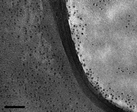 | ||
| Fig. 1 Transmission electron microscope (TEM) image of ZnS:Cu (0.2%) NCs. The scale bar is 50 nm. | ||
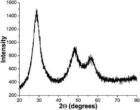 | ||
| Fig. 2 X-Ray diffraction (XRD) pattern of ZnS:Cu (0.2%) NCs. | ||
The UV-Vis absorption spectra of the ZnS:Cu (0.2%) NCs before shell growth and with ZnS monolayers are shown in Fig. 3. The 0 monolayer sample has absorption starting around 330 nm and features a small peak around 300 nm and an apparent strong peak around 240 nm. The peak near 240 nm is an artifact due to the decrease in instrumental response since the real absorption is usually expected to continue to increase towards shorter wavelength. As monolayers are added to the surface of the Cu-doped ZnS NCs, roughly from 2–10 monolayers, the absorption onset and peak at 300 nm are red-shifted, as shown in the inset of Fig. 3. The doping level of Cu did not affect the UV-Vis spectra in any noticeable manner. Overall, there is a small but clear red-shift in the absorption onset due to the increased size of the NCs.
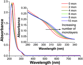 | ||
| Fig. 3 UV-Visible absorption spectra of ZnS:Cu (0.2%) with 0–10 monolayers of a ZnS shell, grown at 100 °C. The inset shows a closer look of the absorption edge of the same spectra. | ||
In contrast to Fig. 3, which shows the UV-Vis of Cu-doped ZnS NCs with a ZnS shell grown at 100 °C, Fig. 4 shows the UV-Vis of Cu-doped ZnS NCs with an attempted ZnS shell grown at room temperature. The absorption of the 0 monolayer sample starts around 330 nm with the lowest energy band peak around 305 nm. As ZnS “monolayers” were added to the Cu-doped ZnS NCs, enough to build a 10 monolayer shell, the absorption peak at 305 nm was blue-shifted to about 294 nm. This blue-shift is an indication of an increase of smaller ZnS NCs being formed due to the nucleation of new ZnS NCs, rather than the formation of a ZnS shell on the already formed ZnS:Cu NCs. Similar evidence of growing smaller NCs rather than a ZnS shell were also observed for growth at 40 °C and 60 °C as well. The contrast between the results in Fig. 3 and 4 suggest that the true monolayer growth of ZnS on ZnS:Cu NCs requires temperature higher than room temperature, and 100 °C is sufficient for the shell growth.
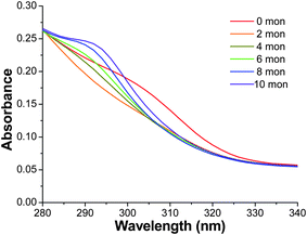 | ||
| Fig. 4 The tail of the UV-visible absorption spectra of ZnS:Cu (0.2%) (same range as inset for Fig. 1) with 0–10 monolayers of a ZnS shell grown at room temperature, rather than the typical synthesis with ZnS shell growth at 100 °C. | ||
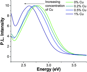
For PL measurements, the NC concentration of each sample was adjusted to be 0.26 in optical density (OD) at 280 nm to make it easier for quantitative comparison. The normalized PL emission spectra of ZnS NCs with 0 monolayer coverage doped with 0%, 0.2%, 0.5%, and 1% Cu are shown in Fig. 5. The undoped ZnS NCs exhibit a peak at 2.79 eV (445 nm) with a FWHM of ∼0.5 eV. The PL emission peak of the 0.2% Cu is slightly red-shifted and exhibits a peak at 2.76 eV (449 nm). The 0.5% Cu NCs peaked at 2.72 (456 nm) and 1% Cu-doped NCs peaked at 2.62 eV (473 nm). There is an apparent emergence of a peak in each spectra starting ∼2.3 eV, which is an artifact resulting from the Rayleigh scattering of the excitation light (λex = 280 nm) with the grating at second order. There is clearly a red-shift in the observed PL emission peak with increased concentration of copper, similar to what we have observed previously.30
 | ||
| Fig. 5 PL emission spectra of core ZnS NCs doped with 0%, 0.2%, 0.5%, and 1% copper with λex = 280 nm; the NC concentration in solution was adjusted so that the optical OD was 0.26 for each sample. | ||
Based on our previous study,30 we know that the PL for the Cu-doped ZnS NCs is composed of emission from trap states of ZnS and emission from the Cu-dopant, with their relative contribution dependent on the Cu doping level. Higher percentages of Cu doping generally led to stronger Cu emission and weaker ZnS emission. In order to better understand the characteristics of these two emissions, the PL of ZnS NCs without Cu doping was also studied. The PL emission spectrum of the undoped ZnS NCs with 0 monolayers is shown in Fig. 6. The PL spectrum is dominated by one major peak positioned at 2.79 eV with a FWHM of ∼0.5 eV, which is due to trap state emission based on the large Stokes shift from the bandgap energy. As monolayers of ZnS were added onto the surface of the ZnS NCs at 100 °C, aliquots were taken every two monolayers and their PL spectra show a small but noticeable red-shift towards lower energy. A representative PL spectrum for the 8 monolayer sample is also shown in Fig. 6, which is red-shifted by about 0.06 eV compared to that with no coverage (0 monolayers). Both PL spectra were fit using single Gaussian functions, as shown in Fig. 6. Details of the fitting are discussed later. Note that the PL intensity generally increases with an increasing number of monolayers. For example, the increase is about 10% for the 8 monolayer coverage compared to 0 monolayers for the undoped sample.
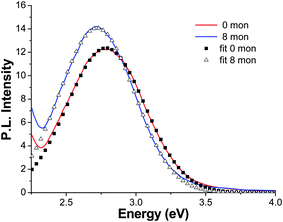 | ||
Fig. 6 The PL emission spectra of undoped ZnS with 0 (![[thick line, graph caption]](https://www.rsc.org/images/entities/char_e117.gif) ) and 8 () monolayers of ZnS and the corresponding single Gaussian fits (■) and (△), respectively. ) and 8 () monolayers of ZnS and the corresponding single Gaussian fits (■) and (△), respectively. | ||
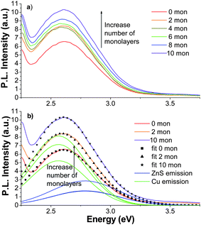
In order to better understand the relative contributions of ZnS trap state emission and Cu dopant emission as well as their respective characteristics with different monolayer coverages, several samples were compared. As shown in Fig. 7a, the PL spectrum for the 0.2% Cu sample with 0 monolayers (no coverage) shows a band peaked at 2.76 eV with a FWHM of ∼0.5 eV. As monolayers were added, the PL emission peak red-shifted and the intensity increased. For 10 monolayer coverage, the PL band peaked at 2.67 eV and displayed an increase in emission intensity of 37% compared to no coverage. Each spectrum with zero through 10 monolayers was fit using two Gaussian functions: one to represent the PL from trap states of ZnS and the second to represent the PL from the Cu-dopant. Parameters for the Gaussian representing the ZnS emission peak position and FWHM are kept the same as those used in Fig. 6. The peak position was allowed to vary between 2.79 eV to 2.72 eV, which were the peak positions for the ZnS emission peak for the undoped sample with zero and ten monolayers. The intensity was then allowed to vary to optimize fitting to the experimental results. The parameters for the Gaussian representing the Cu emission were found by fitting the ZnS:Cu (1%) since its emission is dominated by the Cu emission line. The details of all the fittings will be described in greater detail below. As representative examples for the 0.2% Cu sample, the 0, 2, and 10 monolayer fits are shown in Fig. 7b with points (squares, triangles, and stars); the two constituent peaks correlating with ZnS trap-state emission and Cu-dopant emission are shown as solid green and blue lines.
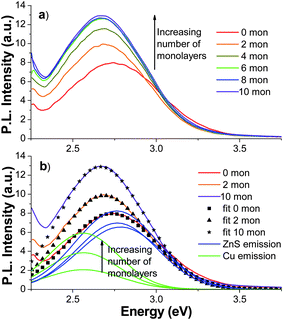 | ||
| Fig. 7 (a) PL emission spectra of ZnS:Cu (0.2%) with 0 (red), 2 (orange), 4 (gold), 6 (green), 8 (blue), and 10 (violet) ZnS monolayers with λex = 280 nm; (b) PL emission of ZnS:Cu (0.2%) with 0, 2, and 10 ZnS monolayers with corresponding two-Gaussian fits, (■), (▲), and (★). The two constituent Gaussians of each fit are shown (the Cu peak is green and the ZnS peak is blue). The peaks increase in intensity with additional monolayers. | ||
Next we investigated the effect of adding monolayers of ZnS to the 0.5% Cu doped NCs. The PL emission spectrum of ZnS:Cu (0.5%) NCs with zero monolayers is shown in Fig. 8a. The spectrum is dominated by a peak at 2.72 eV with a FWHM of ∼0.5 eV. As with the ZnS:Cu (0.2%) sample, the PL emission was red-shifted and the intensity increased with ZnS monolayer addition. The 10 monolayer sample peaked at 2.68 eV and exhibited an increase in emission intensity of 67% compared to the 0 monolayer sample. Each PL emission spectrum was fit with two Gaussian functions. The 0, 2, and 10 monolayer fits and constituent Gaussians are shown in Fig. 8b.
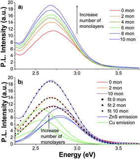 | ||
| Fig. 8 (a) PL emission spectra of ZnS:Cu (0.5%) with 0 (red), 2 (orange), 4 (gold), 6 (green), 8 (blue), and 10 (violet) ZnS monolayers with λex = 280 nm; (b) PL emission of ZnS:Cu (0.5%) with 0, 2, and 10 ZnS monolayers with corresponding two-Gaussian fits, (■), (▲), and (★). The two constituent Gaussians of each fit are shown (the Cu peak is green and the ZnS peak is blue). The peaks increase in intensity with additional monolayers. | ||
The highest dopant concentration of ZnS:Cu that was synthesized was 1% Cu. No higher concentrations of Cu were used due to their instability and decreased luminescence.30 The PL emission spectra of ZnS:Cu (1%) with 0–10 monolayers are shown in Fig. 9a. The zero monolayer NCs PL emission spectrum peaked at 2.62 eV and had a FWHM of ∼0.5 eV. With addition of ZnS monolayers to cover the surface of the doped NCs, the PL emission was very slightly red-shifted. The 10 monolayer coverage sample peaked at 2.61 eV, displaying a shift of only 0.01 eV. The PL emission intensity increased by 57% compared to that of the no coverage sample. Again two Gaussians (at the same positions and with the same widths) were used to fit each PL emission spectra. The 0, 2, and 10 monolayer fits and constituent Gaussians are shown in Fig. 9b.
 | ||
| Fig. 9 (a) PL emission spectra of ZnS:Cu (1%) with 0 (red), 2 (orange), 4 (gold), 6 (green), 8 (blue), and 10 (violet) ZnS monolayers with λex = 280 nm; (b) PL emission of ZnS:Cu (1%) with 0, 2, and 10 ZnS monolayers with corresponding two-Gaussian fits, (■), (▲), and (★). The two constituent Gaussians of each fit are shown (the Cu peak is green and the ZnS peak is blue). The peaks increase in intensity with additional monolayers. | ||
Here we discuss the numerical fitting of the observed PL spectra for the Cu-doped and undoped ZnS NCs. For the undoped NCs, one Gaussian function was used while for each of the ZnS:Cu NCs two Gaussians were used, one representing the ZnS trap state PL and another representing the Cu-dopant PL. This helps to better understand the dependence of the PL on Cu doping level and on the ZnS shell grown around the core doped NCs. In order to find the peak position of ZnS emission, a single Gaussian fit was used for the ZnS with no Cu, as shown in Fig. 6. The 0 monolayer sample had a PL band with a FWHM of ∼0.5 eV and peak position at 2.78 eV. The peak red-shifted with addition of monolayers to 2.72 eV for 8 monolayers of coverage (Fig. 6). The FWHM remains about the same.
Once the parameters for the Gaussian representing the ZnS PL were determined, the ZnS:Cu (1%) PL spectra were used to determine the Gaussian representing the Cu dopant PL. The 1% sample was chosen since the Cu PL was more dominant and the fitting would generate more accurate numbers for the parameters of the Gaussian representing the Cu PL band. The experimental results and fits with two Gaussians for the 1% sample are shown in Fig. 9b. Six data sets (0, 2, 4, 6, 8, 10 monolayers) were fit simultaneously with the location of the ZnS peak allowed to vary slightly between 2.72 eV to 2.78 eV, which was the range found from the undoped ZnS PL emission spectra. For the best fit of the six data sets, the peak for the Cu PL was found to be 2.56 eV (484 nm). The FWHM was found to be ∼0.4 eV. For clarity, only three of these fits, including the two constituent peaks and the overall fit, are included in Fig. 9b.
Once the peak positions and FWHM for both the ZnS and Cu PL bands were determined based on the undoped sample and the 1% doped sample, they were used to fit the ZnS:Cu (0.2%) and ZnS:Cu (0.5%) PL emission spectra. The only adjustable parameters allowed to vary were the relative amplitudes of the two Gaussians representing the relative intensities of the two PL bands. Fig. 7b and 8b show the PL emission spectra with corresponding two Gaussian fits for the ZnS:Cu (0.2%) and ZnS:Cu (0.5%). In the ZnS:Cu (0.2%) fit, shown in Fig. 7b, the Cu emission peak intensity was observed to more than double while the ZnS emission peak only slightly increased. For the ZnS:Cu (0.5%) (Fig. 8b), the Cu emission intensity was again more than doubled, while the ZnS emission was only marginally increased. Likewise, the ZnS:Cu (1%) sample also shows a greater increase in the Cu emission than that of the ZnS emission. The fitting reveals that with addition of a ZnS shell, the Cu emission increased much more than the ZnS trap state emission.
It is interesting to compare quantitatively the intensity of the PL emission in the ZnS NCs doped with various concentrations of Cu and to observe the effect of adding ZnS layers. We focus on 0 and 10 monolayers as examples. The undoped ZnS NCs showed the least increase in PL emission intensity with ZnS shell coverage when compared to the Cu-doped NCs. A summary of the increases in PL emission intensity and red-shift with 10 monolayer addition is shown in Table 1. The increase in PL intensity with monolayer growth of ZnS is dominated by the increase in Cu-dopant PL, which is a desired outcome for doped semiconductor NCs for electroluminescence and other photonics applications, as discussed later.
:Cu NCs
| % Increase | λ (0 mon) | λ (10 mon) | |
|---|---|---|---|
| 0% Cu | 10% | 445 | 456 |
| 0.2% Cu | 37% | 449 | 464 |
| 0.5% Cu | 67% | 456 | 464 |
| 1% Cu | 57% | 473 | 475 |
EXAFS
Examples of the k-space EXAFS results, extracted from the absorption data, are shown in Fig. 10 for the Cu and Zn K-edges. The data for the dilute Cu dopant (obtained in fluorescence mode) are noisier but still have reasonable S/N (signal-to-noise) out to 12 Å−1, while the k-space data for the Zn K-edge have good S/N out to 14 Å−1.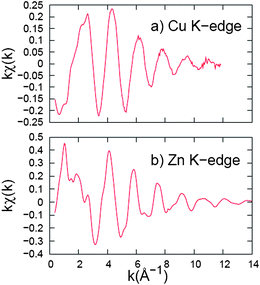 | ||
| Fig. 10
k-Space data for (a) Cu K-edge and (b) Zn K-edge of ZnS:Cu (0.2%). The energy spectrum is converted into momentum-space (k-space) and then is Fourier transformed to position-space (r-space) to show peaks for different shells of neighbors (see Fig. 11 and 12). Note the different vertical scales; the Cu EXAFS scale is a factor of two smaller than for the Zn EXAFS. | ||
Next the k-space data were Fourier transformed to r-space, which show peaks corresponding to different shells of neighbors about either Zn or Cu. The r-space data at the Zn and Cu K-edges, for NC samples doped with 0.2% and 0.5% Cu, are shown in Fig. 11 and 12, respectively. Each plot is an average of three traces. The data for the initial NCs are plotted with a red line while the data for the NCs, after several monolayers have been added, are shown in green.
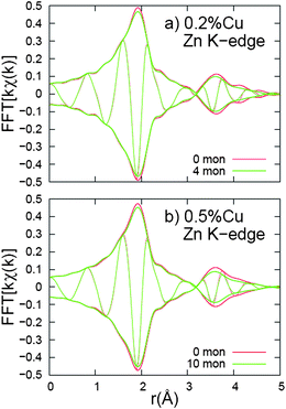 | ||
| Fig. 11 Fourier transform of kχ(k), r-space data, for Zn K-edge. In these (and following) r-space graphs, the rapidly oscillating function is the real part, R, of the FT while the envelope function is ±√{R2 + I2} where I is the imaginary part of the FT. The k-space window is 3.0–14.0 Å−1, with the ends of the window having a Gaussian rounding of 0.3 Å−1. For both Cu concentrations, the additional monolayers cause a slight decrease in both the first and second neighbor peak amplitudes. | ||
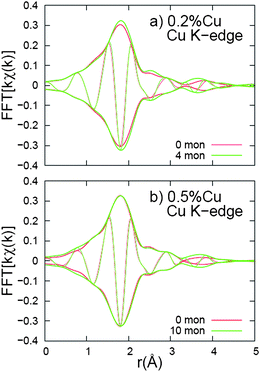 | ||
| Fig. 12 Fourier transform of kχ(k), r-space data, for Cu K-edge. The k-space window is 3.0–10.5 Å−1, with the ends of the window having a Gaussian rounding of 0.3 Å−1. For both Cu concentrations, the additional monolayers cause a very slight increase in the second neighbor peak amplitude. | ||
The Zn K-edge data (Fig. 11) show little change in the r-space data as 4 or 10 monolayers are deposited. These r-space plots are nearly identical to Zn K-edge data reported earlier for ZnS nanoparticles.30 The large amplitude for the Zn–S first peak indicates that the material is reasonably well ordered at the nearest neighbor level, but the small amplitude for the second (Zn–Zn) peak shows that there is considerable disorder at the second neighbor level. For both Cu concentrations, the amplitude is very slightly reduced for both the first (Zn–S) and second (Zn–Zn) peaks, indicating slightly increased disorder of the ZnS host material when monolayers are added. More importantly, the second peak, which corresponds to Zn–Zn pairs, is much smaller than bulk and was expected to grow as the size of the nanoparticles increased, if the nanoparticles had good crystallinity.38
The Cu K-edge data (Fig. 12) also shows little change in the r-space data as 4 or 10 monolayers are deposited. Again the first (Cu–S) peak is large indicating little disorder for the nearest neighbors. However the second neighbor peak (Cu–Zn) is very small and significantly smaller than the (disordered) Zn–Zn peak in the Zn K-edge data. This low amplitude means there is a high degree of disorder for the Cu–Zn second neighbors, or perhaps a decreased number of Zn neighbors. Unlike the Zn K-edge data, the amplitude of the second (Cu–Zn) peak is marginally increased for all the samples when monolayers are added; i.e. the second neighbor distribution becomes slightly more ordered.
Discussion
Enhanced Cu PL emission
One key observation is that for each of the core ZnS NCs, the PL intensity increased with the growth of ZnS shells. To understand the origin of this, it is helpful to examine the intensity increase concurrently with the red-shift in PL emission peak position. The undoped sample had a small red-shift of 11 nm with 10 monolayers of ZnS shell coverage, from 445 nm to 456 nm. This PL red-shift is attributed to the increased size of the NCs with shell growth. When the ZnS NCs were doped with Cu, the PL emission was red-shifted compared to the undoped sample before the ZnS shell was grown (Fig. 5). An even greater red-shift of the PL was apparent in the ZnS:Cu/ZnS NCs when the shell was grown, compared to the undoped NCs. This can be well modeled as an increase in the emission from a Cu center as the thickness of the ZnS shell increases. In contrast, the UV-Vis absorption spectra of the NCs from 0 to 10 monolayers (Fig. 3) are identical for doped and undoped samples, and therefore the size evolution of the undoped and doped NCs are determined to be the same.
The reproducible PL spectral shift of ZnS NCs doped with various concentrations of Cu can be well understood by considering the relative contributions of the ZnS trap state emission versus the Cu dopant emission. Since the increase in PL intensity was much higher and the red-shift with increasing ZnS monolayers was more substantial for the doped samples than the undoped samples, the apparent red-shift is attributed mainly to an increase in Cu PL emission with growth of a ZnS shell. The fit results in Fig. 7–9 show that the Cu-dopant PL emission increases much more than the ZnS host PL emission and the Cu PL band is redder than the ZnS PL band. The overall observed PL band red-shifts as the contribution from the Cu PL increases. This also explains why the PL for the 1% Cu sample red-shifted only slightly since the overall PL emission was already dominated by Cu, before the ZnS shell was grown. Further growth of the ZnS shell has little effect on the position of the Cu PL. In contrast, samples with low Cu doping in which the ZnS PL and Cu PL are both important, the growth of a ZnS shell resulted in relatively stronger Cu emission and thus the appearance of a red-shift. The stronger Cu PL that results from ZnS shell coverage is likely due to surface Cu sites that were not emissive originally but become emissive upon incorporation into the ZnS lattice with further ZnS shell growth. Successful fitting of the PL emission spectra of the Cu-doped ZnS NCs with two Gaussians representing the emission from Cu and the emission from ZnS seem to support the above explanation (Fig. 7b, 8b, and 9).
It is clear from comparing the undoped ZnS PL emission spectra (Fig. 6) with the three ZnS:Cu PL emission spectra and their fits (Fig. 7, 8, and 9) that there is a greater increase in PL emission intensity with ZnS shell addition for the Cu emission center. The increase in Cu emission may be attributed to the addition of a ZnS shell covering non-emissive Cu dopant sites that reside on the surface of the initial ZnS:Cu NCs and essentially make them into part of the core of the NCs. These non-emissive sites were predicted based on EXAFS studies of the core doped particles in our previous work30 in which the large disorder of the second shell around Cu could result from Cu near the surface of the nanoparticle. The conclusion that surface dopant sites are non-emissive while core dopant sites are luminescent has been found for Mn-doped ZnSe NCs previously using combined spectroscopic and EXAFS and ESR studies in our lab.31 This study shows that similar conclusion can be reached for ZnS:Cu NCs, for the first time, to our best knowledge. In addition, we have devised a simple but effective strategy to increase the dopant PL by using a thin layer of undoped host semiconductor to incorporate the original, non-luminescent surface dopant sites. It was further noted that for both the ZnS:Cu (0.2%) and ZnS:Cu (0.5%) NCs, the Cu emission more than doubled upon ZnS shell growth, while the Cu PL peak of the ZnS:Cu (1%) increased by less than expected compared to that of the ZnS:Cu (0.5%) sample. This is likely due to quenching caused by aggregation of the CuS at too high of dopant concentration, again similar to the Mn–Mn quenching observed for ZnSe:Mn.31
Local structure about Zn and Cu
The EXAFS results show that at the nearest neighbor level, the environments about both Zn (host) and Cu (dopant) are quite well ordered. However for the second neighbors (Zn–Zn or Cu–Zn) there is significant disorder; the Zn–Zn peak is significantly smaller than in bulk ZnS and this reduced amplitude cannot be simply explained by the small size of the NCs (4–6 nm). Furthermore, the disorder is slightly larger when monolayers are deposited (which should normally lead to a larger Zn–Zn peak in good crystalline material). This suggests that the deposited ZnS shell is not of high crystallinity. Thus the NCs are either collections of very tiny nanocrystals (∼ 1 nm) or include significant fractions of amorphous phase, or both.The disorder about Cu at the second neighbors is even higher, but surprisingly the Cu–Zn is marginally larger when the ZnS monolayers are added. The high disorder at the second neighbor level is not surprising as Cu prefers the layered CuS structure over the cubic ZnS structure – note that the CuS structure does have a similar tetrahedral arrangement of S around one of the Cu sites. The slight increase in amplitude of the Cu–Zn peak is consistent with the result from the photoluminescence experiments, that the copper is becoming more encapsulated by adding ZnS monolayers.
Combined with the PL data, this suggests that the Cu environment is disordered even when far from the surface of the NCs. Given the small particle size and low Cu concentration, we expect only 2–4 Cu atoms per NC, making it very unlikely to form a Cu–S precipitate. Also, the Cu–S bonds are shorter20 and might strain the ZnS host crystal locally. Because the ZnS NCs have significant disorder and Cu prefers a different local environment to the cubic ZnS structure, the small Cu–Zn peak amplitude likely means that the Cu atoms diffuse to more disordered regions of the NCs.
Conclusion
ZnS:Cu/ZnS core–shell NCs were synthesized via a facile aqueous synthesis. Based on our previous EXAFS studies of the local structure around the Cu-dopant in ZnS:Cu core NCs, some of the Cu was suggested to be at or near the surface of the NCs.30 Dopants at surface sites tend to be non-luminescent and thus undesired for photonics applications that rely on luminescence.31 In order to test if this indeed is the case for ZnS:Cu NCs, a ZnS shell was grown around the Cu-doped ZnS core NCs to determine its effect on the PL properties. The result of shell growth was an amplitude increase and a red-shift of the overall PL of the NCs that was significantly more pronounced for the Cu-doped ZnS NCs than the undoped ZnS NCs. When the PL emission from the doped samples was deconvolved into two PL bands representing the ZnS emission and Cu emission, it became clear that there was a much greater increase in Cu emission than ZnS emission due to ZnS shell growth. This greater increase is attributed to the surface Cu-dopant incorporation into the core ZnS NC lattice aided by the extra ZnS shell.
The EXAFS data indicate that, with added monolayers, Cu has marginally more ordered second neighbors, consistent with increased copper encapsulation. However, adding monolayers of ZnS actually appears to decrease the second neighbor peak slightly, indicating that the additional ZnS is more disordered than the core and may have a significant amorphous fraction. The result of this study is significant in better understanding the fundamental optical properties of doped semiconductor NCs and their dependence on the structural details. It also has important implications in applications in electroluminescence and other photonics devices.
Experimental
Materials
All the chemicals were of reagent grade and used without further purification. 3-Mercaptopropionic acid (MPA, #107-96-0, 99+% purity), sodium sulfide nonahydrate (#1313-84-4, 98+% purity) and sodium hydroxide (NaOH, #1310-73-2, 98.5% purity) were purchased from Acros Organics (Morris Plains, NJ). Zinc nitrate hexahydrate (Zn(NO3)2·6H2O, #10196-18-6, crystalline/certified) was purchased from Fisher Scientific (Pittsburgh, PA). Copper(II) chloride dihydrate (CuCl2·2H2O, #10125-13-0, 99+% purity) was purchased from Sigma-Aldrich (Milwaukee, WI). High purity (>18 Ω cm) Milli-Q water (Millipore, Watford) was used.Synthesis of ZnS![[hair space]](https://www.rsc.org/images/entities/h3_char_200a.gif) :Cu/ZnS nanocrystals
:Cu/ZnS nanocrystals
In a typical synthesis, ZnS:Cu (0.2%) NCs were synthesized according to our previous work.30 The synthesis was slightly modified in that the reaction mixture was brought to reflux, excess Zn was added, and then it was refluxed for 5 min rather than 2 h. The crude reaction mixture was used without purification; however it was allowed to cool to allow for ease of handling, and then 25 ml were extracted and brought back to reflux. 0.15 M Zn(NO3)2 and 0.1 M Na2S/0.04 M MPA/0.08 M NaOH were added to the solution in 200 μL injections with a 30 s interval in between each injection. Five injections of Zn and S were considered to be a one monolayer addition. The assumption that this constitutes one monolayer is based on a calculation using the size of NCs and their concentration in solution to find the total surface area of the NCs and then using that to find the amount of Zn and S that would constitute a single monolayer. The shape of the NCs is generally not a perfect sphere, and thus the ZnS shell cannot be assumed to coat the NCs evenly to make up a perfect monolayer. This term, monolayer, is used only to quantify the amount of Zn and S that are added in comparison to the NCs in solution. Each experiment lasted 50 min, which allowed up to 10 monolayers to be grown onto the NCs. Aliquots were taken from the reaction mixture every two monolayers for spectroscopic analysis.
Instrumentation
Low-resolution TEM measurements were performed on a JEOL model JEM-1200EX microscope. The crystal structure of the samples was characterized by X-ray diffraction (XRD, Rigaku Americas Miniflex Plus powder diffractometer), using Cu-Kα (λ = 1.54056 Å) irradiation. Diffraction patterns were recorded from 20° to 80° 2θ, with a step size of 0.04° at a rate of 2° per minute. The UV-Vis absorption spectra were taken on a Hewlett Packard 8452A Diode Array Spectrophotometer at room temperature. The photoluminescence (PL) spectra were measured on a Perkin Elmer Luminescence Spectrometer LS50B at room temperature. The samples that were analyzed with spectrophotometry were prepared by dispersing the nanoparticles in Milli-Q water, basified to pH ∼11 with NaOH, to yield a clear solution. Centrifugation was performed on a Sorvall Legend RT at 3000 rpm for 10 min at room temperature.EXAFS details
Temperature dependent EXAFS data at the Cu (fluorescence) and Zn (transmission) K-edge for the powdered ZnS:Cu NC samples were collected at the Stanford Synchrotron Radiation Laboratory (SSRL), beamline 10-2. The NCs were collected using filter paper and then encapsulated and sealed in tape. 1–3 layers were used to achieve a reasonable absorption step at the Zn K-edge in transmission mode, yielding step heights of about 0.1–0.5. Data were collected using a silicon [111] double monochromator, detuned 50% to reduce harmonics. Small slits (∼0.5 mm) provided an energy resolution of 1.3 eV. Cu EXAFS data were collected in fluorescence mode using a 13-element Ge fluorescence detector. Both data sets were reduced using standard procedures (RSXAP)39 with a Fourier transform (FT) window of 3.0–10.5 Å−1 for Cu and 3.0–14.0 Å−1 for Zn; the ends of the windows have a Gaussian rounding of 0.3 Å−1. The FT data show peaks in r-space that correspond to shells of neighbors at different distances from the excited atom (Zn or Cu). Note that the peak positions in all EXAFS data are slightly shifted to lower r (by known amounts) compared to the actual bond length.
Acknowledgements
This project is funded by the US Department of Energy (DE-FG02-07ER46388-A002). The EXAFS experiments were performed at SSRL, operated by the DOE, Division of Chemical Sciences, and by the NIH, Biomedical Resource Technology Program, Division of Research Resource. We would also like to thank Mike Kozina for assistance in data fitting.References
- A. I. Ekimov, A. L. Efros and A. A. Onushchenko, Quantum size effect in semiconductor microcrystals, Solid State Commun., 1985, 56, 921 CAS.
- M. Nirmal, B. O. Dabbousi, M. G. Bawendi, J. J. Macklin, J. K. Trautman, T. D. Harris and L. E. Brus, Fluorescence intermittency in single cadmium selenide nanocrystals, Nature, 1996, 383, 802 CrossRef CAS.
- C.-C. Chen, A. B. Herhold, C. S. Johnson and A. P. Alivisatos, Size Dependence of structural metastability in semiconductor nanocrystals, Science, 1997, 276, 398 CrossRef CAS.
- W. C. W. Chan and S. Nie, Quantum dot bioconjugates for ultrasensitive nonisotopic detection, Science, 1998, 281, 2016 CrossRef CAS.
- C. B. Murray, C. R. Kagan and M. G. Bawendi, Synthesis and Characterization of monodisperse nanocrystals and close-packed nanocrystal assemblies, Annu. Rev. Mater. Sci., 2000, 30, 545 CrossRef CAS.
- J. Z. Zhang, Interfacial charge carrier dynamics of colloidal semiconductor nanoparticles, J. Phys. Chem. B, 2000, 104, 7239 CrossRef CAS.
- X. Peng, Mechanisms for the shape-control and shape-evolution of colloidal semiconductor nanocrystals, Adv. Mater., 2003, 15, 459 CrossRef CAS.
- V. I. Klimov, S. A. Ivanov, J. Nanda, M. Achermann, I. Bezel, J. A. McGuire and A. Piryatinski, Single-exciton optical gain in semiconductor nanocrystals, Nature, 2007, 447, 441 CrossRef CAS.
- W. Chen, Nanoparticle self-lighting photodynamic therapy for cancer treatment, J. Biomed. Nanotechnol., 2008, 4, 369 Search PubMed.
- S. C. Erwin, L. Zu, M. I. Haftel, A. L. Efros, T. A. Kennedy and D. J. Norris, Doping semiconductor nanocrystals, Nature, 2005, 436, 91 CrossRef CAS.
- B. A. Smith, J. Z. Zhang, A. Joly and J. Liu, Luminescence decay kinetics of Mn2+-doped ZnS nanoclusters grown in reverse micelles, Phys. Rev. B: Condens. Matter Mater. Phys., 2000, 62, 2021 CrossRef CAS.
- H. Yang, P. H. Holloway and B. B. Ratna, Photoluminescent and electroluminescent properties of Mn-doped ZnS nanocrystals, J. Appl. Phys., 2003, 93, 586 CrossRef CAS.
- R. N. Bhargava, D. Gallagher, X. Hong and A. Nurmikko, Optical properties of manganese-doped nanocrystals of ZnS, Phys. Rev. Lett., 1994, 72, 416 CrossRef CAS.
- M. A. Chamarro, V. Voliotis, R. Grousson, P. Lavallard, T. Gacoin, G. Counio, J. P. Boilot and R. Cases, Optical properties of Mn-doped CdS nanocrystals, J. Cryst. Growth, 1996, 159, 853 CrossRef CAS.
- N. Pradhan, D. M. Battaglia, Y. Liu and X. Peng, Efficient, stable, small, and water-soluble doped znse nanocrystal emitters as non-cadmium biomedical labels, Nano Lett., 2007, 7, 312 CrossRef CAS.
- D. A. Schwartz, N. S. Norberg, Q. P. Nguyen, J. M. Parker and D. R. Gamelin, Magnetic quantum dots: synthesis, spectroscopy, and magnetism of Co2+-and Ni2+-doped ZnO nanocrystals, J. Am. Chem. Soc., 2003, 125, 13205 CrossRef CAS.
- W. Chen, J. Z. Zhang and A. G. Joly, Optical properties and potential applications of doped semiconductor nanoparticles, J. Nanosci. Nanotechnol., 2004, 4, 919 CrossRef CAS.
- R. Revathi and T. R. N. Kutty, Blue ac electroluminescence of Zn1−xMgxS: Cu, Br powder phosphors, J. Mater. Sci., 1986, 21, 2100 CrossRef CAS.
- S. Tanaka, H. Kobayashi, and H. Sasakura, Electroluminescence materials, ed. S. Shionoya and W. M. Yen, 1999 Search PubMed.
- M. Warkentin, F. Bridges, S. A. Carter and M. Anderson, Electroluminescence materials ZnS: Cu, Cl and ZnS: Cu, Mn, Cl studied by EXAFS spectroscopy, Phys. Rev. B: Condens. Matter Mater. Phys., 2007, 75, 75301 CrossRef.
- P. O. Anikeeva, J. E. Halpert, M. G. Bawendi and V. Bulovic, Electroluminescence from a mixed red–green–blue colloidal quantum dot monolayer, Nano Lett., 2007, 7, 2196 CrossRef CAS.
- V. Wood, J. E. Halpert, M. J. Panzer, M. G. Bawendi and V. Bulovicì, Alternating current driven electroluminescence from ZnSe/ZnS: Mn/ZnS nanocrystals, Nano Lett., 2009, 9, 2367 CrossRef.
- N. K. Morozova, V. G. Galstyan and V. I. Muratova, Nature of the inhomogeneities and luminescence centers in low-Ohmic single ZnS crystals doped with Al, Izv. Akad. Nauk SSSR, Neorg. Mater., 1985, 21, 1097 CAS.
- Y. L. Soo, Z. H. Ming, S. W. Huang, Y. H. Kao, R. N. Bhargava and D. Gallagher, Local structures around Mn luminescent centers in Mn-doped nanocrystals of ZnS, Phys. Rev. B: Condens. Matter, 1994, 50, 7602 CrossRef CAS.
- S. Kishimoto, T. Hasegawa, H. Kinto, O. Matsumoto and S. Iida, Effect and comparison of co-doping of Ag, Ag plus In, and Ag+Cl in ZnS: N/GaAs layers prepared by vapor-phase epitaxy, J. Cryst. Growth, 2000, 214–215, 556 CrossRef.
- W. Chen, J. O. Malm, V. Zwiller, Y. Huang, S. Liu, R. Wallenberg, J. O. Bovin and L. Samuelson, Energy structure and fluorescence of Eu2+ in ZnS: Eu nanoparticles, Phys. Rev. B: Condens. Matter Mater. Phys., 2000, 61, 11021 CrossRef CAS.
- P. Yang, M. Lü, D. Xü, D. Yuan and G. Zhou, Photoluminescence properties of ZnS nanoparticles co-doped with Pb2+ and Cu2+, Chem. Phys. Lett., 2001, 336, 76 CrossRef CAS.
- A. A. Khosravi, M. Kundu, L. Jatwa, S. K. Deshpande, U. A. Bhagwat, M. Sastry and S. K. Kulkarni, Green luminescence from copper doped zinc sulfide quantum particles, Appl. Phys. Lett., 1995, 67, 2702 CrossRef CAS.
- D. Jiang, L. Cao, W. Liu, G. Su, H. Qu, Y. Sun and B. Dong, Synthesis and luminescence properties of core–shell ZnS: Mn/ZnO nanoparticles, Nanoscale Res. Lett., 2009, 4, 78 Search PubMed.
- C. Corrado, Y. Jiang, F. Oba, M. Kozina, F. Bridges and J. Z. Zhang, Synthesis, structural, and optical properties of stable ZnS: Cu, Cl nanocrystals, J. Phys. Chem. A, 2009, 113, 3830 CrossRef CAS.
- T. J. Norman, D. Magana, T. Wilson, C. Burns, J. Z. Zhang, D. Cao and F. Bridges, Optical and surface structural properties of Mn2+-doped ZnSe nanoparticles, J. Phys. Chem. B, 2003, 107, 6309 CrossRef.
- L. Cao, J. Zhang, S. Ren and S. Huang, Luminescence enhancement of core–shell ZnS: Mn/ZnS nanoparticles, Appl. Phys. Lett., 2002, 80, 4300 CrossRef CAS.
- Z. Quan, Z. Wang, P. Yang, J. Lin and J. Fang, Synthesis and Characterization of high-quality ZnS, ZnS:Mn2+, and ZnS:Mn2+/ZnS (core–shell) luminescent nanocrystals, Inorg. Chem., 2007, 46, 1354 CrossRef CAS.
- J. Zheng, X. Yuan, M. Ikezawa, P. Jing, X. Liu, Z. Zheng, X. Kong, J. Zhao and Y. Masumoto, Efficient photoluminescence of Mn2+ ions in MnS/ZnS core–shell quantum dots, J. Phys. Chem. C, 2009, 113, 16969 CrossRef CAS.
- J. Nickerson, P. Goldberg and D. H. Baird, The influence of copper on structural transformations in ZnS: Cu, Cl, J. Electrochem. Soc., 1963, 110, 1228 CrossRef CAS.
- M. Aven and J. A. Parodi, Study of the crystalline transformations in ZnS: Cu, ZnS: Ag and ZnS: Cu, Al, J. Phys. Chem. Solids, 1960, 13, 56 CrossRef CAS.
- Y. T. Nien, I. G. Chen, C. S. Hwang and S. Y. Chu, Microstructure and electroluminescence of ZnS: Cu, Cl phosphor powders prepared by firing with CuS nanocrystallites, J. Electroceram., 2006, 17, 299 CrossRef CAS.
- J. Stanley, Y. Jiang, F. Bridges, S. A. Carter and L. Ruhlen, Degradation and rejuvenation studies of AC electroluminescent ZnS: Cu, Cl phosphors, J. Phys.: Condens. Matter, 2010, 22, 055301 CrossRef.
- C. H. Booth, R-Space X-Ray Absorption Package, 2005 Search PubMed.
| This journal is © The Royal Society of Chemistry 2010 |