Patterning of hydrophobic three-dimensional carbon nanotube architectures by a pattern transfer approach†
Jia-Qi
Huang
,
Qiang
Zhang
,
Meng-Qiang
Zhao
,
Guang-Hui
Xu
and
Fei
Wei
*
Beijing Key Laboratory of Green Chemical Reaction Engineering and Technology, Department of Chemical Engineering, Tsinghua University, Beijing, 100084, China. E-mail: wf-dce@tsinghua.edu.cn; Fax: +86-10-6277-2051
First published on 24th June 2010
Abstract
Hydrophobic three-dimensional carbon nanotube architectures with patterned morphologies have been fabricated by a pattern transfer method, in which the components of the masks served as promoters/inhibitors to increase/decrease the catalyst activity for the self-organization of carbon nanotubes into a family of patterned nanoarchitectures.
Creating three-dimensional (3D) patterned nanoarchitectures on the surface of a substrate is an essential step towards the investigations on their novel properties and the developments of nanomaterials and nanodevices at different length scales. Patterned nano-architectures composed of one-dimensional (1D) nanowires/nanotubes on two-dimensional substrates always exhibit tailored mechanical, thermal, catalytic or optical properties.1–5 Among the various 1D nanomaterials, a carbon nanotube (CNT) is one of the most attractive building blocks because of its unique properties originating from its small size, cylindrical structure, and high aspect ratio.1–4 If CNTs can be controllably patterned into 3D nanoarchitectures, they will hold promise for a variety of applications in intelligent nanocomposites with hydrophobic surfaces, field emission display, energy conversion and storage, sensor, and catalysis.1,2,6 It should be noticed that the patterned CNTs are of extremely large surface-to-volume ratios ranging from 5 × 10⁶ to 2 × 10⁷ m2 m−3, which exceeds that of state-of-the-art microreactors by at least two orders of magnitude.1,2 Therefore, 3D patterned CNTs will be an extraordinary platform to demonstrate the advantages of nanoscience, and improve the applications of nanotechnology.4
The facile fabrication of patterned nanoarchitectures is the first step in exploring this fascinating nanotechnology. Over time, lithography, nanocontact printing and writing, and self assembly have become promising techniques for the fabrication of patterned micro/nanostructures. For instance, shadow masking,7 block copolymer micellar thin films,8 soft-lithography,9 and photolithography10 were used to pattern iron catalysts for the self oriented growth of CNT architectures. The substrate can also be modulated into a patterned structure to adjust the relationship between the catalysts and substrate. For example, pyrolysis of xylene/ferrocene on a patterned SiO2/Si substrate realized a site-selective growth of multi-directional aligned CNTs.11 Moreover, various post-transfer techniques, such as microcontact printing,12 mechanical scraping,13 and micromolding techniques were also developed to prepare micropatterns of CNTs aligned in a direction normal to the substrate surface. Various patterned CNT nanostructures have also been fabricated by self-organization through the chemical vapor deposition (CVD) growth. For example, hierarchical 3D tubular micropatterns composed of CNTs were fabricated on silicon substrates by catalytic decomposition of a cyclohexane/ferrocene mixture in the presence of water14 and/or CO2.15 Well-defined carbon polyhedrons with faceted morphologies and hollow internal structures made of self-organized multi-walled CNTs can be obtained by gas phase catalytic CVD inside microchannels.16 Among those strategies mentioned above, the self-organization of CNTs into 3D nanoarchitectures was always sensitive to the design of catalyst layers. How to pattern the catalyst layers is a key issue for 3D patterning of CNT growth.7–10 However, it should be noticed that the activities of catalysts, which can be easily tailored by the composition of catalysts, also played an important role in CNT growth and self-organization. For instance, Mo was always selected as a promoter in porous catalyst to significantly improve the activity of catalysts for high yield growth of CNTs,17 while Au, Cu, K elements were often used as inhibitors to poison the transitional metal nanoparticles in the synthesis of CNTs.18 If we can control the patterning of a promoter/inhibitor on a catalyst layer, patterned growth of CNTs will be realized originating from the differences in catalyst activities. Hence, multi-functional patterned 3D nanoarchitectures could be constructed.
Herein, we describe a facile but effective and efficient microcontact pattern transfer approach to pattern the CNTs through the masking of various patterned masks, and to in situ self-organize CNTs into ordered 3D nanoarchitectures. A family of 3D CNT architectures was synthesized by the introduction of the patterned masks, namely promoter/inhibitor phase. As illustrated in Scheme 1, patterned promoter/inhibitor masks were used to modulate the chemical composition of the catalyst, tune the catalytic activity in the covered area, which resulted in the self-organization of CNTs into various 3D patterned nanoarchitectures. Once a promoter such as Mo grid was covered on the Fe catalyst film, Mo atoms will be transferred onto the Fe film during the high temperature pre-treatment and then high active Fe/Mo alloy phase was patterned on the substrate, leading to the formation of rilievo-structured CNT architectures (Scheme 1b, with higher CNT architectures in the mask-covered areas). If an inhibitor, such as Au, Cu grids were laid on the catalyst layer, the Au, Cu atoms will deactivate the metal catalyst for the growth of CNTs, which may cause the formation of intaglio-structured CNT architectures (Scheme 1d, with lower CNT architectures in the mask-covered areas).
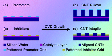 | ||
| Scheme 1 Patterning of 3D CNT architectures by a pattern transfer approach. The substrate with Fe catalyst layer covered by (a) promoter grid led to (b) the formation of rilievo-patterned CNT architectures; while covering by (c) inhibitor grid led to (d) the formation of intaglio-patterned CNT architectures. | ||
The patterning growth of 3D CNT architectures by a pattern transfer approach involved several procedures. A SiO2/Si (600 nm thick thermally grown SiO2 layer) wafer was selected as the substrate. Al2O3 (10.0 nm), Fe (1.0 nm) and MgO (1.0 nm) were sequentially deposited on the substrate as the catalyst film by the electron beam evaporation. The commercial mesh grids with different compositions for transmission electron microscope (TEM) analysis, such as Mo, Au, Cu, Fe, Ni grids, were selected as the masks. Firstly, the TEM grids of various patterned structures were laid onto the surface of MgO/Fe/Al2O3/SiO2/Si substrate. They were then set into a horizontal tubular furnace for the CVD growth of CNTs through the pyrolysis of ethylene. Generally, the temperature of the furnace was raised to 750 °C under Ar atmosphere, and H2 was then introduced to anneal the catalyst film for 10 min before the introduction of ethylene to start the growth of CNTs. After the CVD growth of patterned CNTs, the furnace was cooled down to room temperature under Ar protection. The typical flow rates for Ar, H2, and ethylene were 250, 200, and 100 sccm, respectively. The as-obtained products were characterized using scanning electron microscopy (SEM, JSM 7401F), TEM (JEM 2010), Raman spectrophotometer (Renishaw RM2000 with laser excitation line at 633.0 nm), X-ray photoelectron spectroscopy (XPS, PHI Quantera SXM), and contact angle meter (Dataphysics OCA20 with 2 μL pure water drops).
To demonstrate the above mentioned concept, rectangular patterned Mo/Au girds were selected as the promoter/inhibitor to illustrate the pattern transfer strategy. The patterns of the as-used grids were illustrated in Fig. S1 in the ESI.†Fig. 1a-b showed the related self-organized 3D CNT architectures. With the masking of Mo grids as the promoters, patterned CNT architecture was obtained, indicating the Mo grid tuned the growth behaviors of CNTs obviously. Without the cover of Mo grids, the Fe catalyst gave rise to the growth of short CNT films.7,19 When covered with grid lines of Mo grids, the aligned CNTs showed higher growth rate originated from the higher catalytic activities with the promotion of Mo doping into the metal catalyst. Consequently, there existed a growth rate difference between the CNT arrays that the CNTs under the covering grow faster. During the growth of CNT arrays, the stress accumulated due to this rate difference, which caused the split of the top surface of the array and the growth towards outsides. The CNT arrays under the cover of grid crosses also split outwards, and some long aligned CNT arrays stood as pillars because of the relatively large area (Fig. S2a in the ESI†). The cover of Mo grids altered the growth rate of CNT arrays and constructed a hierarchical CNT architecture through multi-directional growth during the 10-min CVD process. Fig. 1b shows the patterned CNT films with the cover of Au grids as inhibitors. The pattern of Au grid was transferred onto the CNT films that CNTs can hardly grow under the cover of Au grid while dense and short CNT arrays can be synthesized without the coverage. Therefore, the pattern of Au grids, the shape of lines and symbols on Au gird were replicated onto the aligned CNTs. It was worth mentioning that the edge of pattern was sharp and the resolution of Au induced patterning reached 10 μm, which was limited by the available structure of the patterned grid in this contribution.
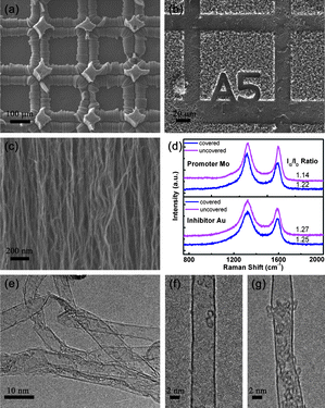 | ||
| Fig. 1 (a) A promoter (Mo grid) patterned growth of rilievo-structured CNT architectures; (b) an inhibitor (Au grid) patterned growth of intaglio-structured CNT architectures; (c) the SEM micrograph of the aligned CNTs in promoter patterned growth; (d) Raman spectra of CNT arrays obtained in the Mo and Au patterned CVD process; (e) TEM and (f), (g) high resolution TEM micrographs of patterned aligned CNTs under the Mo grid mask. | ||
With detailed SEM characterization, CNTs were found to retain their alignments during the patterned mask assistant self-organization process (Fig. 1c). To compare the qualities of CNTs in covered and uncovered areas, Raman spectra of CNTs in different areas were presented in Fig. 1d. The Raman spectra of CNTs showed two main peaks: the D peak around 1325 cm−1 and the G peak around 1580 cm−1, corresponding to the signal of disordered and ordered graphite structures, respectively. The intensity ratio of the G peak to the D peak (IG/ID) was widely used in determining the graphitization degree of the CNTs. It was noticed that the Raman spectra of samples with and without the cover of patterned grids showed similar band shapes. When the CNTs were synthesized under the cover of Mo and Au grids, the IG/ID ratios of CNTs changed slightly from 1.14 to 1.22, 1.27 to 1.25, respectively. This indicated that the graphitization of CNTs was slightly better when Mo served as the promoter, while was a little worse when Au served as the inhibitor for CNT growth. As indicated by the TEM images (Fig. 1e–g), the 3D CNT architecture derived on Mo grid was mainly composed of single-walled CNTs. The diameters of the CNTs were relatively large. Generally, no significant difference between the structures of CNTs with and without the cover of micro grids was observed.
We have successfully demonstrated that patterned promoter (Mo grid) and inhibitor (Au grid) masks can assist the formation of rilievo- and intaglio-patterned CNT architectures, respectively. Other masks including Cu, W, and Ni grids were also tested, and inhibitor effects were also illustrated (Fig. S3 in the ESI†). Compared with other patterning methods for CNT growth, this pattern transfer approach was much more convenient in controlling the patterns of promoter/inhibitor and therefore the pattern of catalyst activities, leading to the fabrication of controllable 3D CNT architectures.
The Mo mask assisted growth was further selected as a model to investigate the mechanism of patterned growth. XPS spectra were employed to decide whether Mo, the second active phase, was transferred onto the Fe catalyst layer. After the annealing process, the XPS spectrum of Mo covered area showed an obvious Mo 3d peak, while no Mo signal can be detected on the area without the cover of Mo grids (Fig. 2a). The insert showed the fine scan of Mo signal area and the content of Mo on covered area were estimated to be 0.61%. During the heating process, molybdenum oxides on the Mo grid diffused onto catalyst film in contact with Mo grid (covered area). The addition of small amount of Mo into Fe catalysts can stabilize the catalyst particles and form new phases that were more active in the synthesis of CNTs.17,20 This improved the activity of Fe catalyst and extended the growth window for CNT arrays. Besides, the pressure applied onto the aligned CNTs was reported to affect the growth behavior of CNT arrays.21 To exclude this factor, a substrate was annealed with Mo grid first, then the Mo grid was removed before CNT growth. Higher CNT arrays still formed according to the grid pattern during the annealing process (Fig. 2b) despite the removal of Mo grid during the CVD growth of CNTs. However, it should be noticed that the structure of CNT array was quite different from that in Fig. 1a. Patterning growth of CNTs was not that obvious compared with the pattern obtained in Fig. 1a. The diffusion of the promoter component (Mo) on the surface in extra cooling and heating process were responsible for this growth phenomenon, which reduced the differences in catalytic growth of CNTs. While for the inhibitor assisted growth of patterning CNTs, the catalyst activity correspond to the inhibitor deceased due to the chemical doping of Au, Cu, etc. onto Fe catalyst layers.18 This was also verified by the growth of CNTs with a separate annealing process of Au grid (similar to that in Fig. 2b), in which CNT films can hardly be synthesized in the covered area though inhibitor grid was removed after the annealing process (not shown). The lower catalytic activities caused the formation of thinner CNT films, leading to the formation of an intaglio-structured CNT architecture.
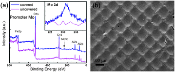 | ||
| Fig. 2 (a) The XPS spectra on annealed silicon substrate, showing the Mo signal on covered area, the insert showed enlarged spectra in Mo 3d region; (b) the obtained CNT on substrate annealed with patterned Mo mask, while the Mo grid was removed during the CVD process. | ||
Based on the understanding of this process, a family of CNT nanoarchitectures can be designed. Using Mo as a growth switch, walnut-like CNT architectures (Fig. 3a) were obtained on solely inactive thin Fe catalyst layer (0.5 nm), with 3 min annealing and 10 min growth. In this pattern, CNT protuberance formed in the places corresponded to the cross areas in the Mo grid. It was supposed that the sublimation of Mo in these areas realized the growth of these periodic CNT patterns, while inadequate Mo sublimation failed to support the growth of CNT architectures. The multi-directional growth behavior was also observed due to the higher growth rates with the assistance of Mo content (Fig. S2b in the ESI†). With prolonged annealing duration (10 min), CNT monolith can be fabricated as shown in Fig. 3b. Long annealing duration ensured the migration of adequate Mo onto the catalyst films covered by both grid lines and crosses, so that grid-patterned monolith constructed by CNT arrays (200 μm in 10 min growth) can be fabricated. After the peeling off of this CNT monolith, only thin CNT films were found in the holes without the cover of Mo grid (Fig. S4 in the ESI†). The growth rate of aligned CNTs covered by the mask was estimated to be two orders of magnitude higher than that without the cover.
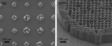 | ||
| Fig. 3 Different CNT architectures obtained with Mo grid as the mask. (a) Walnut-like CNT architectures with 3-min annealing; (b) CNT monolith obtained with 10-min annealing. | ||
Combining the outstanding properties of pristine CNTs and the hierarchical structures, the CNT architectures obtained by the pattern transfer process were demonstrated to be of attractive properties. For instance, the introduction of hierarchical CNT architectures can improve the hydrophobic property of CNT films.22 The pristine substrate after the deposition of catalyst films showed a contact angle of 81° (Fig. 4a), which increased to 140°(Fig. 4b) after the synthesis of uniform CNT films. A contact angle of 152° on the surface of CNT monolith (see Fig. 3b) was shown in Fig. 4c, indicating that the surface of hierarchical CNT structures was more hydrophobic than uniform CNT films. Moreover, the CNT monolith exhibited the advantages of multi-stage structure,2,23 and was promising as a new nanomaterial for micro-reactors serving under extreme conditions. Finally, the patterned area of CNTs was limited by the size of available grid masks (3 mm in diameter), and the CNT films were relatively uniform in this area. If large-area masks for the pattern transfer approach can be obtained through micromachining, then the CNT nanoarchitectures were anticipated to be produced in large scale.
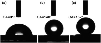 | ||
| Fig. 4 The contact angle of water drop (2 μL) on different substrates: (a) the catalyst substrate; (b) normal CNT array; (c) CNT monolith. | ||
In summary, a novel approach to constructing various 3D patterned CNT nanoarchitectures through a pattern transfer method was reported. Utilizing masks such as Mo, Au, Cu, W, and Ni micro grids, the promoter/inhibitor phase can be patterned onto the catalyst layer and rilievo- or intaglio-structured CNT nano-architectures formed. The synergetic effect of chemical doping and gravity induced assembling were speculated to be responsible for the complex self-organization. The as-obtained CNT nanoarchitectures showed super-hydrophobic properties. A facile alternative approach for constructing a family of functional CNT architectures were demonstrated, which will benefit the exploration of the nanoscale science and technology.
The work was supported by the Foundation for the Natural Scientific Foundation of China (No. 20736004, No. 20736007, No. 2007AA03Z346), the China National Program (No. 2006CB0N0702).
References
- (a) N. Ishigami, H. Ago, Y. Motoyama, M. Takasaki, M. Shinagawa, K. Takahashi, T. Ikuta and M. Tsuji, Chem. Commun., 2007, 1626 RSC; (b) A. Popp and J. J. Schneider, Angew. Chem., Int. Ed., 2008, 47, 8958 CrossRef CAS.
- A. Popp, O. Yilmazoglu, O. Kaldirim, J. J. Schneider and D. Pavlidis, Chem. Commun., 2009, 3205 RSC.
- (a) C. Liu, F. Li, L. P. Ma and H. M. Cheng, Adv. Mater., 2010, 22, E28 CrossRef CAS; (b) D. S. Su and R. Schlogl, ChemSusChem, 2010, 3, 136 CrossRef CAS; (c) X. C. Gui, J. Q. Wei, K. L. Wang, A. Y. Cao, H. W. Zhu, Y. Jia, Q. K. Shu and D. H. Wu, Adv. Mater., 2010, 22, 617 CrossRef CAS.
- J. Khanderi, R. C. Hoffmann and J. J. Schneider, Nanoscale, 2010, 2, 613 RSC.
- Q. Zhang, J. Q. Huang, M. Q. Zhao, Y. Wang, W. Z. Qian and F. Wei, Carbon, 2008, 46, 1152 CrossRef CAS.
- (a) R. T. Lv, F. Y. Kang, D. Zhu, Y. Q. Zhu, X. C. Gui, J. Q. Wei, J. L. Gu, D. J. Li, K. L. Wang and D. H. Wu, Carbon, 2009, 47, 2709 CrossRef CAS; (b) R. T. Lv, S. Tsuge, X. C. Gui, K. Takai, F. Y. Kang, T. Enoki, J. Q. Wei, J. L. Gu, K. L. Wang and D. H. Wu, Carbon, 2009, 47, 1141 CrossRef CAS; (c) E. J. Garcia, B. L. Wardle, A. J. Hart and N. Yamamoto, Compos. Sci. Technol., 2008, 68, 2034 CrossRef CAS; (d) N. Yamamoto, A. J. Hart, E. J. Garcia, S. S. Wicks, H. M. Duong, A. H. Slocum and B. L. Wardle, Carbon, 2009, 47, 551 CrossRef CAS.
- (a) S. S. Fan, M. G. Chapline, N. R. Franklin, T. W. Tombler, A. M. Cassell and H. J. Dai, Science, 1999, 283, 512 CrossRef CAS; (b) K. Hata, D. N. Futaba, K. Mizuno, T. Namai, M. Yumura and S. Iijima, Science, 2004, 306, 1362 CrossRef CAS.
- R. D. Bennett, A. J. Hart, A. C. Miller, P. T. Hammond, D. J. Irvine and R. E. Cohen, Langmuir, 2006, 22, 8273 CrossRef CAS.
- S. M. Huang, A. W. H. Mau, T. W. Turney, P. A. White and L. M. Dai, J. Phys. Chem. B, 2000, 104, 2193 CrossRef CAS.
- S. M. Huang, L. M. Dai and A. W. H. Mau, Adv. Mater., 2002, 14, 1140 CrossRef CAS.
- B. Q. Wei, R. Vajtai, Y. Jung, J. Ward, R. Zhang, G. Ramanath and P. M. Ajayan, Nature, 2002, 416, 495 CrossRef CAS.
- (a) S. M. Huang, L. M. Dai and A. W. H. Mau, J. Phys. Chem. B, 1999, 103, 4223 CrossRef CAS; (b) C. L. Pint, Y. Q. Xu, S. Moghazy, T. Cherukuri, N. T. Alvarez, E. H. Haroz, S. Mahzooni, S. K. Doorn, J. Kono, M. Pasquali and R. H. Hauge, ACS Nano, 2010, 4, 1131 CrossRef CAS.
- (a) J. B. Yang, L. M. Dai and R. A. Vaia, J. Phys. Chem. B, 2003, 107, 12387 CrossRef CAS; (b) R. Xiang, T. Z. Wu, E. Einarsson, Y. Suzuki, Y. Murakami, J. Shiomi and S. Maruyama, J. Am. Chem. Soc., 2009, 131, 10344 CrossRef CAS.
- Z. B. Zhao, J. Y. Qu, J. S. Qiu, X. Z. Wang and Z. Y. Wang, Chem. Commun., 2006, 594 RSC.
- J. Qu, Z. Zhao, Z. Wang, X. Wang and J. Qiu, Carbon, 2010, 48, 1465 CrossRef CAS.
- J. Y. Qu, Z. B. Zhao, J. S. Qiu and Y. Gogotsi, Chem. Commun., 2008, 2747 RSC.
- (a) C. L. Pint, Y. Q. Xu, M. Pasquali and R. H. Hauge, ACS Nano, 2008, 2, 1871 CrossRef CAS; (b) Q. Zhang, M. Q. Zhao, J. Q. Huang, Y. Liu, Y. Wang, W. Z. Qian and F. Wei, Carbon, 2009, 47, 2600 CrossRef CAS; (c) Q. Zhang, M. Q. Zhao, Y. Liu, A. Y. Cao, W. Z. Qian, Y. F. Lu and F. Wei, Adv. Mater., 2009, 21, 2876 CrossRef CAS.
- A. Y. Cao, X. F. Zhang, C. L. Xu, J. Liang, D. H. Wu and B. Q. Wei, Appl. Surf. Sci., 2001, 181, 234 CrossRef CAS.
- (a) C. L. Pint, N. T. Alvarez and R. H. Hauge, Nano Res., 2009, 2, 526 Search PubMed; (b) J. Q. Huang, Q. Zhang, M. Q. Zhao and F. Wei, Nano Res., 2009, 2, 872 Search PubMed; (c) K. Liu, Y. H. Sun, L. Chen, C. Feng, X. F. Feng, K. L. Jiang, Y. G. Zhao and S. S. Fan, Nano Lett., 2008, 8, 700 CrossRef CAS.
- (a) Q. Zhang, M. Q. Zhao, J. Q. Huang, J. Q. Nie and F. Wei, Carbon, 2010, 48, 1196 CrossRef CAS; (b) A. J. Hart, A. H. Slocum and L. Royer, Carbon, 2006, 44, 348 CrossRef CAS; (c) H. Yoshida, T. Shimizu, T. Uchiyama, H. Kohno, Y. Homma and S. Takeda, Nano Lett., 2009, 9, 3810 CrossRef CAS.
- A. J. Hart and A. H. Slocum, Nano Lett., 2006, 6, 1254 CrossRef CAS.
- (a) L. Feng, S. H. Li, Y. S. Li, H. J. Li, L. J. Zhang, J. Zhai, Y. L. Song, B. Q. Liu, L. Jiang and D. B. Zhu, Adv. Mater., 2002, 14, 1857 CrossRef CAS; (b) T. L. Sun, H. A. Liu, W. L. Song, X. Wang, L. Jiang, L. Li and D. B. Zhu, Angew. Chem., Int. Ed., 2004, 43, 4663 CrossRef CAS; (c) J. Q. Huang, Q. Zhang, G. H. Xu, W. Z. Qian and F. Wei, Nanotechnology, 2008, 19, 435602 CrossRef.
- (a) A. J. Hart, L. van Laake and A. H. Slocum, Small, 2007, 3, 772 CrossRef CAS; (b) J. Amadou, D. Begin, P. Nguyen, J. P. Tessonnier, T. Dintzer, E. Vanhaecke, M. J. Ledoux and C. Pham-Huu, Carbon, 2006, 44, 2587 CrossRef CAS; (c) B. B. Gong, R. Wang, B. Y. Lin, F. Me, X. J. Yu and K. M. Wei, Catal. Lett., 2008, 122, 287 CrossRef CAS.
Footnote |
| † Electronic supplementary information (ESI) available: Additional SEM images. See DOI: 10.1039/c0nr00203h |
| This journal is © The Royal Society of Chemistry 2010 |