A highly sensitive ultraviolet sensor based on a facile in situ solution-grown ZnO nanorod/graphene heterostructure†
Haixin
Chang
a,
Zhenhua
Sun
b,
Keith Yat-Fung
Ho
c,
Xiaoming
Tao
a,
Feng
Yan
*b,
Wai-Ming
Kwok
*c and
Zijian
Zheng
*a
aNanotechnology Center, Institute of Textiles and Clothing, The Hong Kong Polytechnic University, Hung Hom, Kowloon, Hong Kong SAR. E-mail: tczzheng@inet.polyu.edu.hk
bDepartment of Applied Physics, The Hong Kong Polytechnic University, Hung Hom, Kowloon, Hong Kong SAR. E-mail: apafyan@polyu.edu.hk
cDepartment of Applied Biology and Chemical Technology, The Hong Kong Polytechnic University, Hung Hom, Kowloon, Hong Kong SAR. E-mail: bcwmkwok@inet.polyu.edu.hk
First published on 25th October 2010
Abstract
The weak photon absorption and fast carrier kinetics of graphene limit its application in photodetection. This limitation can be overcome by introducing photosensitive nanostructures to graphene. Herein we report the synthesis of a ZnO nanorod/graphene heterostructure by a facile in situ solution growth method. By combining the attributes of photosensitive ZnO nanorods and highly conductive graphene, we for the first time demonstrate a highly sensitive visible-blind ultraviolet (UV) sensor based on graphene related heterostructure. The photoresponsibility of the UV sensor can reach 22.7 A W−1, which is over 45,000 fold higher than that of single graphene sheet based photodetectors.
1. Introduction
Graphene is a novel carbon nanomaterial with a unique two-dimensional conjugated structure and electronic properties, and has been intensively studied for applications in electronic devices, nanocomposites, solar cells and sensors.1–17 Very recently, a rapidly increasing interest has been focused on graphene based photodetectors. For example, an all-spectrum ultrafast photodetector was developed from mechanically exfoliated single layer graphene, while the photoresponsibility was only limited to 0.1–0.5 mA W−1 because of the weak light absorption and fast charge carrier kinetics of graphene.18 To increase the photosensitivity, photo-sensitive nanomaterials such as quantum dots (QDs) or nanoparticles were introduced to graphene to form functional composite materials.10,19,20 For instance, we have demonstrated that in situ grown CdS QD/graphene heterostructures could work as efficient photoelectrochemical cells which had a high on-off optical switch.10 Geng et al. prepared non-covalently linked CdSe QD/graphene hybrids that exhibited rapid photo-responsive properties.20 All these graphene based heterostructures or composites were developed for the detection of visible light. However, to the best of our knowledge, no work is reported on the detection of ultraviolet (UV) light with graphene based heterostructures or composites to date, although UV sensors are highly desirable in many fields such as flame detection, environmental studies, medical and communication equipment.21,22Herein, we demonstrate for the first time the development of visible-blind, UV sensors on the basis of thin films of ZnO nanorod/graphene heterostructures, which are synthesized by a facile in situ aqueous seeded growth method. Because of the wide bandgap (∼3.37 eV), ZnO nanostructures are ideal UV-sensitive semiconductors for optoelectronic applications.23–27 In the heterostructure reported here, ZnO nanorods function as UV absorbing and charge carrier generating materials, while graphene obtained by chemical reduction of graphene oxide is used as a charge transporting, highly conductive matrix. The photoresponsibility of the as-made UV sensor can reach 22.7 A W−1 at 20 V bias, which is over 45,000 folds higher than that of single graphene sheet based photodetectors (∼0.1–0.5 mA W−1).18 More importantly, our device shows little response to visible light, critical for sensitive and selective UV sensors.
2. Results and discussion
2.1 Preparation of ZnO nanorod/graphene heterostructure
Fig. 1 shows a schematic illustration of the fabrication of ZnO nanorod/graphene heterostructures. Firstly, highly water soluble, chemically derived graphene was synthesized by a method we developed previously.28 In the meantime, ZnO QDs were synthesized by a non-aqueous method in methanol. The graphene was then mixed with ZnO QDs in a certain ratio to form a mixture solution, which is subsequently cast onto different substrates including glass, quartz, SiO2/n-Si and polyethylene terephthalate (PET), to yield thin films of ZnO QD/graphene. The films were annealed at a low temperature (100 °C) to evaporate the water and to enhance the adhesion to substrates. The sample was then immersed in a zinc nitrate solution for in situgrowth of ZnO nanorods from the ZnO QD seeds to yield the ZnO nanorod/graphene heterostructures (Fig. 1A). Finally, the sample was rinsed extensively with water several times to get rid of the loosely attached ZnO nanorods. For UV sensor fabrication, gold electrodes with 100 μm channel length were patterned onto ZnO QD/graphene before the in situ hydrothermal growth of ZnO nanorods (Fig. 1B).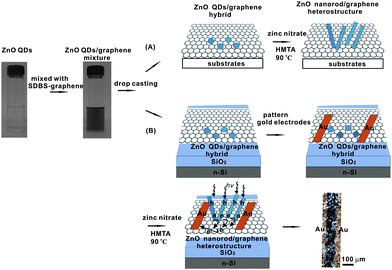 | ||
| Fig. 1 Schemes for facile synthesis of ZnO nanorod/graphene heterostructures from solution processable ZnO QD/graphene hybrid (A) on various substrates and (B) on SiO2/n–Si substrate for thin film optoelectronic devices. Upon irradiation with ultraviolet photons, photogenerated electrons will be transported from ZnO nanorods to graphene and further transported to electrodes by graphene with high efficiency. Therefore the ZnO nanorod/graphene heterostructure here can work as a prototype ultraviolet sensor. | ||
For facile device fabrication and application purposes, it is very important to obtain highly soluble and large size graphene. In our synthetic strategy, graphite oxide was exfoliated and reduced at the presence of sodium dodecylbenzene sulfonate (SDBS) into chemically reduced graphene (SDBS-graphene).28 The single layer SDBS-graphene is typically ∼10 μm in size, and thicker than the mechanically exfoliated one due to the absorption of SDBS (Fig. 2A).28 Measured by tapping mode atomic force microscopy (AFM), single layer and bilayer SDBS-graphene are ca. 2.5 and 5.3 nm thick, respectively (Fig. 2B). Transmission electron microscopy (TEM) and its diffraction analysis (Fig. 2C) confirms the high-quality monolayer structure in most of our samples.29 Importantly, the SDBS-graphene can be readily dissolved in water because of the electrostatic charges on the graphene surface induced by SDBS, to form an aqueous solution as concentrated as 1 mg mL−1 (Fig. 2D).28,30,31
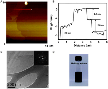 | ||
| Fig. 2 Tapping mode AFM image (A) and depth profile (B) of SDBS-graphene on Si substrate; (C) TEM micrograph and electron diffraction pattern (Inset) of SDBS-graphene; (D) digital image of 1 mg mL−1SDBS-graphene aqueous solution. | ||
The SDBS-graphene was mixed with ZnO QDs in a weight ratio of 1.5 (ZnO to SDBS-graphene) in a methanol–water mixture to yield a grey color solution. The ZnO QDs prepared by non-aqueous method have diameters of 5–10 nm with a lattice spacing of 0.286 nm (Fig. S1, ESI†).32 The mixture was centrifuged and washed several cycles to remove the excess amount of ZnO QDs. TEM images shows that ZnO QDs are indeed uniformly dispersed on the SDBS-graphene surfaces, and few free ZnO QDs is found (Fig. 3A–3C). The diffraction pattern of ZnO QDs on graphene further shows a crystal structure of ZnO QDs (inset in Fig. 3C).33 The fact that ZnO QD/graphene hybrids can be well-preserved after extensive rinsing and centrifuge indicates a strong binding between the ZnO QDs and SDBS-graphene. Considering that the preparation conditions are mild and both the ZnO QDs and SDBS-graphene are negatively charged, we believe that the strong binding force should be attributed to hydrogen bonds and van der Waals interactions. We also believe that the hybrid formation is assisted by the highly wrinkled nature and great flexibility of graphene (due to its two-dimensional sheet structure with one-atom thickness) so that conformal contact between ZnO QDs and SDBS-graphene can be readily made. The ZnO QD/graphene hybrid has a broad UV-vis absorption ranging from 225 nm to 550 nm, in which the 320 nm shoulder peak is attributed to the adsorption of ZnO QDs while the rest of the majority is attributed to the adsorption of SDBS-graphene (Fig. S2A†).
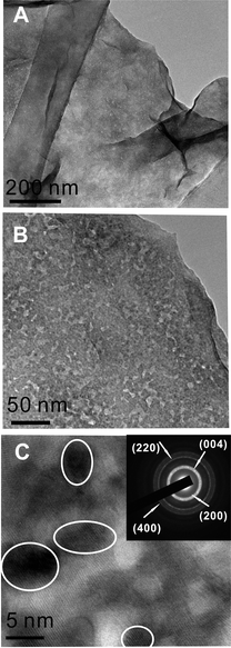 | ||
| Fig. 3 TEM micrograph of ZnO QD/graphene hybrid at low resolution (A, B) and high resolution (C), inset, electron diffraction of ZnO QDs on graphene. | ||
ZnO QD/graphene hybrid film was readily made by casting the mixing solution onto substrates by methods including drop-casting, spincoating, and dip-coating. Typically, we found spincoating and dip-coating of ZnO QD/graphene end up with very thin films of poor coverage of the substrate. Therefore, we adopted drop-casting technique to generate hybrid thin films of ten to several tens of nanometres thick to ensure the formation of a continuous film over 100 μm, which is the distance between gold electrodes of UV sensor as discussed below. The as-made hybrid film is very rough and has many wrinkles through all the surfaces (Fig. 4A and 4B). The thin films were then annealed at 100 °C in an oven for ∼30 min to evaporate the solvent and to enhance the adhesion to the substrates. Note that this step is critical to prevent the scaling of hybrid films from the substrates, which ensure success of the subsequent growth of ZnO nanorods.
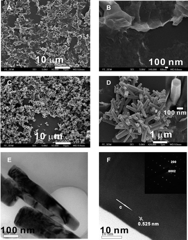 | ||
| Fig. 4 Low (A) and high (B) resolution SEM micrographs of ZnO QD/graphene hybrid film; low (C) and high (D) resolution SEM micrographs of ZnO nanorod/graphene heterostructure; low (E) and high (F) resolution TEM micrographs of ZnO nanorods, inset of (F), electron diffraction pattern of a single ZnO nanorod. | ||
ZnO nanorods can grow in situ from ZnO QDs of the hybrid to form ZnO nanorod/graphene heterostructures.34 As a proof-of-concept, the ZnO QD/graphene coated substrate was immersed in an aqueous solution containing 0.025 M Zn(NO3)2 and 0.025 M hexamethylenetetramine (HMTA) at 90 °C for 1 h. Because of the wrinkled and rough morphology of the hybrid template, ZnO nanorods grew upward to all the directions (Fig. 4C and 4D). The ZnO nanorods have a diameter of 50–200 nm and length of 500 nm–1 μm. High resolution scanning electron microscopy (SEM) image shows an enlarged single ZnO nanorod with hexagonal section morphology, indicating a good degree of crystallization of the nanorods (inset in Fig. 4D). TEM microscopy further confirm that the ZnO nanorods are single crystals and they grow along the c-axis with a lattice spacing of 0.525 nm (Fig. 4E and 4F), typical of single crystal ZnO nanorods.35 We observe some random ZnO nanorods on top of substrate surfaces that are not covered with ZnO QD/graphene. We believe that it is induced by some residue ZnO QDs on the substrate which initiates the ZnO nanorods growth. We also observe that the ZnO nanorods only grow from the top layer of the hybrid film. Considering of a large amount of ZnO QDs embedded in the hybrid film, a possible explanation is that the hybrid film becomes highly compact after thermal annealing, and the surface growth of ZnO nanorods suppresses the diffusion of Zn2+ and HMTA into the inner layers.34 Importantly, the ZnO nanorods have a strong absorption ranging from 305 nm to 375 nm with a peak centered at 350 nm (Fig. S2B†). Compared with ZnO QDs, such a red shift in absorption is more desirable for applications as near UV sensors. More importantly, the absorption at visible light regime is much lower than that at UV regime, indicating that the heterostructure should have high selectivity in the photoresponsibility of the UV regime.
2.2 Fabrication and performance of ZnO nanorod/graphene UV sensor
The heterostructure is ideal for use as the active layer in visible-blind, UV sensitive photodetectors. Therefore, we tested the hypothesis by fabricating ZnO nanorod/graphene based sensors using a photoconductor configuration, in which the substrate was SiO2/n–Si, and the electrodes were gold. Typically, the ZnO QD/graphene hybrid film was prepared on SiO2/n–Si substrates by the above procedures, followed by thermal evaporation of gold through a patterned mask to generate patterned gold electrodes of 100 μm long and 2 mm wide (Fig. 1B). The ZnO nanorod/graphene heterostructure was then formed in the channels by in situ seeded growth method described above. As a proof-of-concept, we use the as-made optoelectronic device to detect 370 nm light by exposing the device under control light intensity while recording the output current (I) of the gold electrodes. In a typical experiment, I was recorded to be ∼300 μA at 20 V bias when the device was not irradiated with the UV light. Upon radiation, I increased monotonically as the 370 nm light power was raised from 0 to 1.084 mW cm−2 (Fig. 5A and 5B). For example, I increased by 16 μA and 52.7 μA at 20 V bias when the UV light power are 65.2 μW cm−2 and 1.084 mW cm−2, respectively. The UV sensor can achieve 6–7 folds higher photocurrent (both in 20 V and ∼0.8 mW cm−2 radiation) than almost the best pure ZnO nanomaterials based traditional metal-semiconductor-metal photodetectors.36 The current increase can be explained by the addition of photogenerated electrons from ZnO nanorods and efficient charge collection and transport of graphene. When the ZnO nanorods are irradiated with UV light, hole and electron pairs will be generated. Because ZnO is an electron transporting material, photogenerated electrons can readily flow into the SDBS-graphene through graphene/ZnO junctions. The SDBS-graphene can then transport the photogenerated charge carriers effectively to the gold electrodes because of its high electronic mobility and conductivity.10,19,20 As a result, a net increase in the output current is recorded.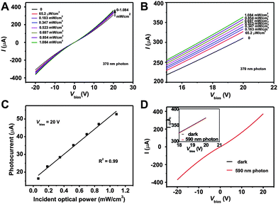 | ||
| Fig. 5 (A) Current versus voltage curves for ZnO nanorod/graphene heterostructures under dark and different power 370 nm photon radiation from 0 to 1.084 mW cm−2, (B) an enlarged view of (A) with Vbias from 15 V to 20 V, (C) photocurrent (the current increase under photon radiation) as a function of incident optical power at 20 V bias, (D) Current versus voltage curves for ZnO nanorod/graphene heterostructure under dark and 108.5 μw/cm2 590 nm photon radiation. Inset: enlarged view of (D) with Vbias from 18 V to 20 V. | ||
Having proven that the ZnO nanorod/graphene heterostructure is highly responsive to 370 nm UV light, we then systematically examined the device performance. The amount of current increase under radiation (compared with the current in dark at 20 V) is plotted against the power of the incident UV light. This calibration curve shows a strong linear relationship with a linear coefficient R2 = 0.99 (Fig. 5C), indicating that our ZnO nanorod/graphene based optoelectronic device can potentially be utilized as a quantitative UV sensor. Importantly, the device does not have photoresponse to visible 590 nm light, which is attributed to the wide energy bandgap in ZnO so that no carrier is excited at low-energy visible photons (Fig. 5D). This characteristic is critical to the applications in highly selective visible-blind UV sensors. The device achieves as high as 22.7 A W−1 efficiency at 20 V bias, over 45000 folds higher than that of single layer graphene photodetectors (∼0.1–0.5 mA W−1).18 Compared with photodetector using pure ZnO nanostructures as the active layer (which achieved 61 A W−1 at 120 V),36 our UV sensor can maintain relatively high efficiency under a low driving voltage, which is a significant advantage in areas such as flexible electronics and wearable electronics.
As control, on the other hand, ZnO QD/graphene hybrid film shows much weaker photoresponse to 370 nm light. With the same device architecture and testing method, only 820 nA increase in photocurrent is recorded at 20 V bias, corresponding to a photoresponsibility of 0.35 A W−1 (Fig. 6A and 6B). The weakening in UV absorption can be partly attributed to the weak absorption of ZnO QDs at 370 nm. As expected, there is no photoresponse to visible 590 nm photons for ZnO QD/graphene hybrid either (Fig. S3†). Further control experiments show that pure SDBS-graphene film has no responses to either 370 nm or 590 nm photons (Fig. 6C, 6D and Fig. S4†). Therefore, we can conclude that the majority of photogenerated current comes from the ZnO nanorod/graphene heterostructures, rather than ZnO QDs or SDBS-graphene.
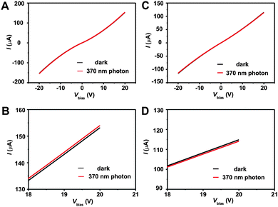 | ||
| Fig. 6 Current versus voltage curves for ZnO QD/graphene hybrid (A, B) and pure SDBS-graphene (C, D) in the dark and under 1.084 mW cm−2 370 nm photon radiation. | ||
We further investigated the kinetic behavior of photoresponses in more detail. Time-resolved photoresponses of ZnO nanorod/graphene, ZnO QD/graphene, and pure SDBS-graphene films were recorded at 5 V bias with 1.084 mW cm−2 power 370 nm light. Fig. 7 shows the background-subtracted time-resolve photoresponse curves of the three devices. As expected, devices with pure SDBS-graphene does not show any increase in photocurrent. A much faster photoresponse for the ZnO nanorod/graphene heterostructure is observed, compared with that of ZnO QD/graphene hybrid. Immediately after irradiation, a very steep current increase is observed for ZnO nanorod/graphene heterostructure based device, with a tangent angle of almost 90°. On the other hand, the current increase of ZnO QD/graphene based device is much more gentle. Several situations may contribute to the faster responses of ZnO nanorod/graphene heterostructure under 370 nm. First, similar to the case of in situ grown CdS QD/graphene heterostructure, in situ hydrothermal growth of ZnO nanorods on graphene will obtain better connection between ZnO nanorods and graphene than the connection between ZnO QDs and graphene formed by simple mixing.10 Second, we find the dark current of the same device increase by 50–150% after hydrothermal growth of ZnO nanorods in 90 °C solution. This may be induced by further reduction and conductivity improvement of SDBS-graphene in the process of hydrothermal growth of ZnO nanorods.37–39 The higher electron conductivity of graphene will facilitate the photogenerated electrons transport to electrodes. Note that time-resolved photoresponse further confirmed that there are no photocurrent generation for ZnO nanorod/graphene heterostructure, ZnO QD/graphene hybrid and pure SDBS-graphene films under 590 nm radiations (Fig. S5†).
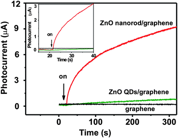 | ||
| Fig. 7 Background-subtracted time-resolved photoresponses of pure SDBS-graphene, ZnO QD/graphene hybrid and the ZnO nanorod/graphene heterostructure at 1.084 mW cm−2 370 nm radiation with Vbias of 5 V. Inset, an enlarged view of the exact starting point when light is on. | ||
Another aspect for the time-resolved photoresponses in ZnO nanorod/graphene heterostructure is the slow photocurrent decay after the UV light is turned off (Fig. S6†). To explore this issue, time-resolved photoluminescence (PL) of ZnO nanorod/graphene heterostructure were investigated on quartz substrate by ultrafast time-resolved emission spectroscopy experiments as we described elsewhere (Fig. 8).40–42 Energy gap PL emission at 385 nm was observed and it decayed dramatically in the time-resolved PL spectra from 1 to 100 ps probe time delay (Fig. 8A).41 No obvious defect emission at 450–700 nm was observed because of the high quality single crystal structure of the ZnO nanorods (Fig. 4E and 4F).43 The PL decay dynamics in Fig. 8B shows that the ZnO nanorods in ZnO nanorod/graphene heterostructures (averaged time constant, 9.2 ps) have almost the same decay properties as the pure ZnO nanorods (averaged time constant, 8.5 ps), which is consistent with a previous report in the averaged time constant of ZnO nanorods.41 Previously, both we and Cao et al. have reported the rapid PL decay of CdS QDs in the in situ grown CdS QD/graphene heterostructures, compared with the pure CdS QDs. The faster decay was attributed to the large contact areas between in situ grown CdS QDs and graphene, and the resulting efficient quenching.10,19 In the present ZnO nanorod/graphene heterostructure, 500 nm to 1 μm long nanorods only contact the SDBS-graphene with one end, a very small part of the nanorods. Therefore the photogenerated carriers may be kept trapped within the ZnO for a long time before it is injected into SDBS-graphene, leading to the slow saturation in photocurrent and the slow decay in output current when the light is turned off.
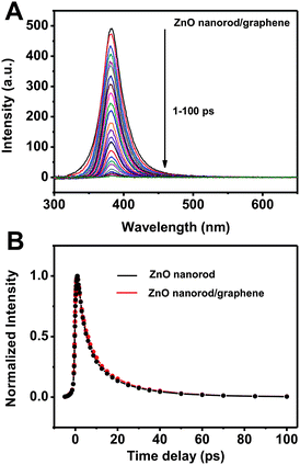 | ||
| Fig. 8 (A) Time-resolved photoluminescence spectra of ZnO nanorods in ZnO nanorod/graphene heterostructure on quartz substrate with 1 to 100 ps time delay after excitation at 267 nm. (B) Photoluminescence decay at 385 nm of pure ZnO nanorods and ZnO nanorods in ZnO nanorod/graphene heterostructures on a quartz substrate. | ||
3. Conclusions and outlook
In summary, we have demonstrated the facile synthesis of ZnO nanorod/graphene heterostructures on various substrates via a seeded solution growth method. Thin-film photoconductors based on ZnO nanorod/graphene heterostructure were for the first time explored as visible-blind UV sensors, which reached a photoresponsibility of 22.7 A W−1 at 20 V. Such a high sensitivity is attributed to the UV absorbing properties of ZnO and the high electron accepting and transporting properties of graphene. Importantly, the UV sensor had no response to visible light and can be used in UV only photodetectors. More importantly, the whole fabrication procedure was carried out in solutions and at mild temperatures. Further considering the transparent and flexible attributes of graphene, our approach should be adaptable to flexible and wearable electronic devices. Note that the prototype UV sensor was tested for 370 nm photons due to the feasibility and availability of the equipment. But according to the absorption spectrum of ZnO nanorods in Fig. S2B,† the UV sensor should have better performance to 350 nm and deeper UV light. Currently, the detection limit is ∼65.2 μW cm−2, i.e., 130.4 nW taking into account the device architecture. We believe that this method can be extended for developing other photosensitive heterostructures (infrared or deep-UV) between graphene and many one-dimensional nanomaterials, for instance, PbS, Si and GaN nanowires by choosing proper nucleation templates on graphene.4. Experimental
Materials and chemicals
Graphite powder (325 mesh, 99.95%) and SDBS (PB, 97%) were purchased from Alfa Aesar (USA). Methanol, zinc nitrate (Zn(NO3)2), and zinc acetate (Zn(AC)2) were purchased from Uni-Chem Chemical Reagents with 99% purity. Hexamethylenetetramine (HMTA) (99% purity) was purchased from Sigma-Aldrich. Other reagents were purchased from Beijing Chemicals Co. Ltd. (China) with analytical grade. All reagents were used as received. Deionized (DI) water was used in all the aqueous solutions.Synthesis of SDBS-graphene and ZnO QDs
Graphite was first oxidized to graphite oxide by Hummer method, and then exfoliated by sonication in the presence of SDBS to form graphene oxide.9,10,28 The graphene oxide was then chemically reduced by hydrazine to form SDBS-graphene following the method we previous published.22 In brief, 1 mg mL−1graphite oxide solution was ultrasonicated in the presence of 1–12 mg mL−1 SDBS for 2 h until no obvious sediment of graphite oxide. The above exfoliated solution was chemically reduced by hydrazine at 100 °C for 12 h. The black precipitate, being SDBS-graphene, was collected by filtration followed by washing with deionized water thoroughly. ZnO QDs were synthesis following a literature procedure.26 In general, 62.5 mL 0.01 M Zn(AC)2 methanol solution was kept at 60 °C and 32.5 mL 0.03 M NaOH was added to the solution drop by drop with strong stirring. The reaction last for over 3 h to ensure the formation of ZnO QDs.Preparation of ZnO QD/graphene hybrid and ZnO nanorod/graphene heterostructures
175 μL 1 mg mL−1SDBS-graphene aqueous solution was added to 1 mL ZnO QDs methanol solution followed by vigorous shaking. The ZnO QD/graphene hybrid was centrifuged and washed with DI-water and methanol several times, and re-dispersed in methanol–water solution. The mixture solution of ZnO QD/graphene can form thin films by drop casting on various substrates such as silicon, glass, quartz and polyethylene terephthalate (PET). The hybrid film was further annealed at 100 °C for ca. 30 min to enhance its adhesion to the substrate. ZnO nanorods were then in situ grown from the graphene using the ZnO QD seeds. The growth of ZnO nanorod/graphene heterostructure was conducted in the 0.025 M Zn(NO3)2 and 0.025 M HMTA at 90 °C for 1 h.34 To fabricate UV sensors, the thin film of ZnO QD/graphene hybrid was prepared on SiO2/n–Si substrate followed by 100 °C annealing. Then it was patterned by gold electrodes with 100 μm channel length and 2 mm width. The patterned ZnO QD/graphene hybrid thin film was placed in the solution of 0.025 M Zn(NO3)2 and 0.025 M HMTA at 90 °C for 1 h to grow ZnO nanorods.Characterizations and measurements
The samples for AFM characterization (tapping mode) were prepared by dropping diluted SDBS-graphene solution on a Si substrate followed by gentle drying. Transmission electron microscopy (TEM) images were collected by JEM-2010 (JEOL) with accelerated voltage of 120 kV. The SEM micrographs were recorded by scanning electron microscopy (SEM) JSM-6301F (JEOL). The UV-Vis spectra were obtained from a Perkin–Elmer spectrophotometer. The experimental setup for time-resolved photoluminescence measurements was described elsewhere.40–42 The thin film device measurements for photonic responses were conducted in nitrogen atmosphere to exclude the influence of oxygen for the convenience of understanding the device physics. The photon irradiation was provided by 370 nm or 590 nm light-emitting diodes (LEDs). No degradation of graphene or damage of devices was found after irradiation (Fig. S7†). The electronic and optoelectronic data of the UV sensors was recorded by an Agilent 4156C Precision Semiconductor Parameter Analyzer. For ultrafast photoluminescence measurements, the samples were prepared on quartz substrates.Acknowledgements
We thank Jinhua Li for the ZnO TEM analysis and discussion. Z.J.Z., H.X.C., and X.M.T. acknowledge The Hong Kong Polytechnic University (Project A-PJ49) for financial support of this work. Z.H.S is financially supported by the Research Grants Council (RGC) of Hong Kong, China (Project B-Q10T).Notes and references
- A. K. Geim and K. S. Novoselov, Nat. Mater., 2007, 6, 183 CrossRef CAS.
- Y. B. Zhang, Y. W. Tan, H. L. Stormer and P. Kim, Nature, 2005, 438, 201 CrossRef CAS.
- S. S. Yu and W. T. Zheng, Nanoscale, 2010, 2, 1069 RSC.
- X. L. Li, X. R. Wang, L. Zhang, S. W. Lee and H. J. Dai, Science, 2008, 319, 1229 CrossRef CAS.
- S. Stankovich, D. A. Dikin, G. H. B. Dommett, K. M. Kohlhaas, E. J. Zimney, E. A. Stach, R. D. Piner, S. T. Nguyen and R. S. Ruoff, Nature, 2006, 442, 282 CrossRef CAS.
- F. Li, Y. Huang, Q. Yang, Z. Zhong, D. Li, L. Wang, S. Song and C. Fan, Nanoscale, 2010, 2, 1021 RSC.
- X. Wang, L. J. Zhi and K. Müllen, Nano Lett., 2008, 8, 323 CrossRef CAS.
- Y. Huang, X. Dong, Y. Shi, C. M. Li, L. J. Li and P. Chen, Nanoscale, 2010, 2, 1485 RSC.
- H. X. Chang, L. H. Tang, Y. Wang, J. H. Jiang and J. H. Li, Anal. Chem., 2010, 82, 2341 CrossRef CAS.
- H. X. Chang, X. J. Lv, H. Zhang and J. H. Li, Electrochem. Commun., 2010, 12, 483 CrossRef CAS.
- A. Reina, X. T. Jia, J. Ho, D. Nezich, H. B. Son, V. Bulovic, M. S. Dresselhaus and J. Kong, Nano Lett., 2009, 9, 30 CrossRef CAS.
- B. Li, X. Cao, H. G. Ong, J. W. Cheah, X. Zhou, Z. Yin, H. Li, J. Wang, F. Boey, W. Huang and H. Zhang, Adv. Mater., 2010, 22, 3058 CrossRef CAS.
- J. Liu, Z. Yin, X. Cao, F. Zhao, A. Ling, L. Xie, Q. L. Fan, F. Boey, H. Zhang and W. Huang, ACS Nano, 2010, 4, 3987 CrossRef CAS.
- J. Liu, Z. Lin, T. Liu, Z. Yin, X. Zhou, S. Chen, L. Xie, F. Boey, H. Zhang and W. Huang, Small, 2010, 6, 1536 CrossRef CAS.
- Q. He, H. G. Sudibya, Z. Yin, S. Wu, H. Li, F. Boey, W. Huang, P. Chen and H. Zhang, ACS Nano, 2010, 4, 3201 CrossRef CAS.
- Z. Yin, S. Wu, X. Zhou, X. Huang, Q. Zhang, F. Boey and H. Zhang, Small, 2010, 6, 307 CrossRef CAS.
- Z. J. Wang, X. Z. Zhou, J. Zhang, F. Boey and H. Zhang, J. Phys. Chem. C, 2009, 113, 14071 CrossRef CAS.
- F. N. Xia, T. Mueller, Y. M. Lin, A. Valdes-Garcia and P. Avouris, Nat. Nanotechnol., 2009, 4, 839 CrossRef CAS.
- A. N. Cao, Z. Liu, S. S. Chu, M. H. Wu, Z. M. Ye, Z. W. Cai, Y. L. Chang, S. F. Wang, Q. H. Gong and Y. F. Liu, Adv. Mater., 2010, 22, 103 CrossRef CAS.
- X. M. Geng, L. Niu, Z. Y. Xing, R. S. Song, G. T. Liu, M. T. Sun, G. S. Cheng, H. J. Zhong, Z. H. Liu, Z. J. Zhang, L. F. Sun, H. X. Xu, L. Lu and L. W. Liu, Adv. Mater., 2010, 22, 638 CrossRef CAS.
- E. Munoz, E. Monroy, J. L. Pau, F. Calle, F. Omnes and P. Gibart, J. Phys.: Condens. Matter, 2001, 13, 7115 CrossRef CAS.
- S. Liang, H. Sheng, Y. Liu, Z. Huo, Y. Lu and H. Shen, J. Cryst. Growth, 2001, 225, 110 CrossRef CAS.
- H. Kind, H. Q. Yan, B. Messer, M. Law and P. D. Yang, Adv. Mater., 2002, 14, 158 CrossRef CAS.
- Z. L. Wang and J. H. Song, Science, 2006, 312, 242 CrossRef CAS.
- B. Weintraub, Z. Zhou, Y. Li and Y. Deng, Nanoscale, 2010, 2, 1573 RSC.
- J. B. Baxter and E. S. Aydil, Appl. Phys. Lett., 2005, 86, 053114 CrossRef.
- Q. H. Li, T. Gao, Y. G. Wang and T. H. Wang, Appl. Phys. Lett., 2005, 86, 123117 CrossRef.
- H. X. Chang, G. F. Wang, A. Yang, X. M. Tao, X. Q. Liu, Y. D. Shen and Z. J. Zheng, Adv. Funct. Mater., 2010, 20, 2893 CrossRef CAS.
- Y. Hernandez, V. Nicolosi, M. Lotya, F. M. Blighe, Z. Y. Sun, S. De, I. T. McGovern, B. Holland, M. Byrne, Y. K. Gun'ko, J. J. Boland, P. Niraj, G. Duesberg, S. Krishnamurthy, R. Goodhue, J. Hutchison, V. Scardaci, A. C. Ferrari and J. N. Coleman, Nat. Nanotechnol., 2008, 3, 563 CrossRef CAS.
- D. Li, M. B. Müller, S. Gilje, R. B. Kaner and G. G. Wallace, Nat. Nanotechnol., 2008, 3, 101 CrossRef CAS.
- X. Y. Qi, K. Y. Pu, X. Z. Zhou, H. Li, B. Liu, F. Boey, W. Huang and H. Zhang, Small, 2010, 6, 663 CrossRef CAS.
- C. Pacholski, A. Kornowski and H. Weller, Angew. Chem., Int. Ed., 2002, 41, 1188 CrossRef CAS.
- H. M. Xiong, Y. Xu, O. G. Ren and Y. Y. Xia, J. Am. Chem. Soc., 2008, 130, 7522 CrossRef CAS.
- L. Vayssieres, Adv. Mater., 2003, 15, 464 CrossRef CAS.
- J. H. He, J. H. Hsu, C. W. Wang, H. N. Lin, L. J. Chen and Z. L. Wang, J. Phys. Chem. B, 2006, 110, 50 CrossRef CAS.
- Y. Z. Jin, J. P. Wang, B. Q. Sun, J. C. Blakesley and N. C. Greenham, Nano Lett., 2008, 8, 1649 CrossRef CAS.
- Y. Zhou, Q. L. Bao, L. A. L. Tang, Y. L. Zhong and K. P. Loh, Chem. Mater., 2009, 21, 2950 CrossRef CAS.
- H. Zhang, X. J. Lv, Y. M. Li, Y. Wang and J. H. Li, ACS Nano, 2010, 4, 380 CrossRef CAS.
- P. V. Kamat, J. Phys. Chem. Lett., 2010, 1, 520 Search PubMed.
- W. M. Kwok, C. S. Ma and D. L. Phillips, J. Am. Chem. Soc., 2006, 128, 11894 CrossRef CAS.
- W. M. Kwok, A. B. Djurisic, Y. H. Leung, W. K. Chan and D. L. Phillips, Appl. Phys. Lett., 2005, 87, 223111 CrossRef.
- W. M. Kwok, C. S. Ma and D. L. Phillips, J. Phys. Chem. B, 2009, 113, 11527 CrossRef CAS.
- L. E. Greene, M. Law, J. Goldberger, F. Kim, J. C. Johnson, Y. F. Zhang, R. J. Saykally and P. D. Yang, Angew. Chem., Int. Ed., 2003, 42, 3031 CrossRef CAS.
Footnote |
| † Electronic supplementary information (ESI) available: A TEM image of ZnO QDs. UV-Vis spectra of ZnO QDs, graphene and ZnO QD/graphene hybrid in methanol–water solution and ZnO nanorods on quartz substrates. I–V curves for ZnO QD/graphene hybrid under dark and 590 nm photon radiation. I–V curves for SDBS-graphene film under dark and 590 nm photon radiation. Time-resolved photoresponses of the ZnO nanorod/graphene heterostructure, ZnO QD/graphene hybrid and pure SDBS-graphene. Time-resolved photoresponses and photocurrent decay of the ZnO nanorod/graphene heterostructure. SEM image of the ZnO nanorod/graphene heterostructure device after irradiated with long term UV light. See DOI: 10.1039/c0nr00588f |
| This journal is © The Royal Society of Chemistry 2011 |
