Nanomechanical architecture of semiconductor nanomembranes
Minghuang
Huang
*a,
Francesca
Cavallo
a,
Feng
Liu
b and
Max G.
Lagally
a
aUniversity of Wisconsin-Madison, Madison, WI 53706, USA. E-mail: mhhuang@cae.wisc.edu
bUniversity of Utah, Salt Lake City, UT 84112, USA
First published on 28th October 2010
Abstract
Semiconductor nanomembranes are single-crystal sheets with thickness ranging from 5 to 500nm. They are flexible, bondable, and mechanically ultra-compliant. They present a new platform to combine bottom-up and top-down semiconductor processing to fabricate various three-dimensional (3D) nanomechanical architectures, with an unprecedented level of control. The bottom-up part is the self-assembly, via folding, rolling, bending, curling, or other forms of shape change of the nanomembranes, with top-down patterning providing the starting point for these processes. The self-assembly to form 3D structures is driven by elastic strain relaxation. A variety of structures, including tubes, rings, coils, rolled-up “rugs”, and periodic wrinkles, has been made by such self-assembly. Their geometry and unique properties suggest many potential applications. In this review, we describe the design of desired nanostructures based on continuum mechanics modelling, definition and fabrication of 2D strained nanomembranes according to the established design, and release of the 2D strained sheet into a 3D or quasi-3D object. We also describe several materials properties of nanomechanical architectures. We discuss potential applications of nanomembrane technology to implement simple and hybrid functionalities.
 Minghuang Huang | Minghuang Huang is a scientist in the Materials Science and Engineering Department at the University of Wisconsin-Madison. His current research interests include nanomechanical architectures of strained Si/Ge nanomembranes and novel nanostructured materials for thermoelectric devices. He received his B.S. degree in Chemistry from the National Tsing-Hua University, Taiwan, R.O.C., and his M.S. and Ph.D. degrees in Materials Science and Engineering from the University of Utah. He has been a process engineer at United Microelectronic Corporation (UMC), Hsinchu, Taiwan, R. O. C. and a senior engineer at Fairchild Semiconductor, Salt Lake City, Utah. |
 Francesca Cavallo | Francesca Cavallo is a post-doctoral fellow in the Materials Science and Engineering Department at the University of Wisconsin-Madison. Her research focuses on fabrication, modeling and characterization of semiconductor based nanostructures for highly integrative applications. She received her Ph.D. degree in Electrical Engineering and Information Technology with magna cum laude from the Technical University of Chemnitz (Germany). She conducted her research studies for her Ph.D. degree at the Max Planck Institute for Solid State Research (Stuttgart, Germany) and at Institute for Integrative Nanosciences (Dresden, Germany). She received her M.S. in Electrical Engineering with highest honors from the University of Salerno (Italy). |
 Feng Liu | Feng Liu is a professor in the Department of Materials Science and Engineering at the University of Utah. His research interests lie in materials modeling and simulation from the atomic to mesoscopic scales, with a recent focus on properties of surfaces, interfaces and nanostructures, mechanisms of growth of thin films and of self-assembly of nanostructures, and nanomechanical architectures of nanomembranes. Liu received his Ph.D. degree in Chemical Physics from Virginia Commonwealth University and was a postdoctoral research fellow at Rutgers University and Oak Ridge National Lab. He has authored 140 publications and holds 4 patents. He received the Humboldt Senior Research Award in 2008. |
 Max G. Lagally | Max G. Lagally is the Erwin W. Mueller Professor of Materials Science and Physics at the University of Wisconsin-Madison. His research focuses on growth and structure-properties relationships of materials at the nanoscale, primarily semiconductors. He received his B.S. degree from the Pennsylvania State University and his Ph.D. degree from Wisconsin, both in physics. He has been a Humboldt Fellow at the Forschungszentrum, Jülich, Germany. He is a member of the U.S. National Academy of Engineering and the German National Academy of Sciences - Leopoldina, and has received numerous other awards. He has founded two companies, nPoint, Inc. and SonoPlot, Inc. |
1. Introduction
The nanotechnology era, born in the 1980s with the development of scanned-probe techniques to visualize structures at the sub-nanometer scale, has brought many innovations in materials and processes. Those having the highest scientific impact were frequently based on self-assembly or “bottom-up” methods: quantum dot growth,1,2 nanowire,3,4 or nanotube growth,5 and DNA or other organic-molecule-based architectures.6 The difficulty with all these methods is, of course, that they are stochastic, and thus have a variation in nanostructural parameters like size, shape, position, and composition. Concurrently, “top-down”, lithography-based processes, which can produce thousands of the same structures and do not suffer from stochasticity, have continued to make significant progress, but it has been obvious that a combination of these methods can provide powerful advances in nanotechnology and in understanding behaviors at the nanoscale. A new platform developed in the last decade, semiconductor nanomembranes, has significantly advanced the ability to combine bottom-up and top-down semiconductor processing to fabricate various three-dimensional (3D) nano- and micro-objects with an unprecedented level of control.7–20 The bottom-up part is the self-assembly, via folding, rolling, bending, curling, or other forms of shape change of the nanomembranes, with top-down processing providing the starting point for the self-assembly. The geometry, mechanical and thermal stability, and unique properties of these self-assembled nanomembranes have suggested new mechanical,12,13 optical,14,15 and electronic17 devices, as well as more complex hybrid functions such as drug delivery,18 micro-reactors,18 scaffolds for cell culture,19 and opto-fluidic components.20Bending, rolling, or folding of nanometer-thick membranes is a response to the release of a large amount of internal potential energy in a constrained film upon the removal of the constraint. This potential energy can be stored in various ways, e.g., by mechanical stress, by surface tension, by a magnetic or electric field, or by chemical modification of the surfaces of the membrane.
We review here stress-driven formation of 3D and quasi-3D micro- and nanomechanical architectures. Nature provides many examples of stress-driven actuation. The Venus flytrap, for example, has a simple system based on hydrostatic pressure and release of stored elastic energy.21 When resting, the two leaves of the hinged trap are open in a concave shape to admit unsuspecting insects. When an intruding fly touches trigger hairs inside the trap, movement of fluid within leaf cells builds up elastic strain in the leaves. When the leaves can no longer sustain the strain, they snap into their other stable shape, curving inward to form a concave enclosure. When fruits or vegetables dry out the turgor pressure is relieved and the tissue starts to wrinkle; on the other hand, when they are preserved in a humid environment cracks form as a result of the increase of the turgor by transpiration. Corrugation and cracking of thin films are other examples of stress-driven phenomena. The delamination of vacuum-deposited metal thin films is caused by large internal stresses arising during the deposition.22,23A significant effort has been directed to minimizing the internal stress of deposited thin films,24 because typically it is desired that the film adhere well without cracks or delamination.
In contrast, within the nanomembrane platform, stress actuation has been translated into a way to fold nm-thickness films into micro- and nanomechanical objects.7 A simple example is a bilayer with one layer intentionally deposited with more residual stress than the lower layer. When this bilayer film is released from the holding substrate (the central feature of the nanomembrane technology), the intrinsic stress gradient established in the bilayer material during deposition drives the defined film to curl in a predictable fashion. Uniform compressive strain in a single-crystalline thin film has been achieved by epitaxial growth on a substrate with a smaller lattice constant or vice versa for tensile strain. A membrane that is uniformly compressively strained relaxes by lateral expansion when it is released from the holding substrate, and the opposite for a tensilely strained single-layer membrane. A bilayer with different strains in the two layers will change its shape to relax the strain when it is released from the holding substrate. Formation of wrinkle-like structures occurs upon partial release of a compressively strained film, as the released regions expand to relax strain. A trilayer membrane in which the top and bottom layers are balanced will, like a single layer, expand or contract, depending on the sign of the strain.
Extensive work has been done since 2000 to achieve control of these phenomena. These efforts succeeded in transforming a trial and error process into a nanofabrication technique for reliable and parallel mass production of identical mixed-dimension nano- and microstructures. A variety of nanomechanical architectural designs has been realized with various materials, including semiconductors,7–11 metals,25 organic materials,26 and insulators,27 as well as combinations of them.12,13,27
Because strain relaxation is the driving force for bending 2D strained sheets or ribbons into 3D structures, the design principles for fabrication of different classes of 3D nanoarchitectures can be described based on total strain energy minimization within the elastic regime. Different nanoshapes can be designed using the geometric and elastic properties of membranes and the magnitude of the gradient of built-in strain.11,28,29 A freestanding strained membrane attached at one end can bend or wrinkle, depending on magnitude of strain and elastic properties of the material. In the bending regime it is possible to tune the radius of curvature by varying the amplitude of the strain gradient and the film thickness. Similarly, in the wrinkling regime the amplitude of wrinkled structures and the spacing between adjacent wrinkles depend on intrinsic parameters, such as the intensity of the strain field and film thickness. Continuum elasticity theory is used to establish generic design principles (i.e., universal physical conditions and geometric relationships) that control the size of nanostructures in a single class, as well as the formation of different classes of nanostructures.11,29–37 Definition of extrinsic parameters, such as the geometry of the film before release, the alignment of the starting edge for the etching process in a certain crystallographic direction, and the etching rate of the sacrificial layer can be used to design the desired ultimate 3D structure.
All-semiconductor membranes with thicknesses ranging from a few to hundreds of nanometers and the proper strain gradients roll up in tubular structures with diameters scalable from tens of micrometers down to 10 nm. Rolled-up tubes are robust and stable. High-resolution transmission electron microscopy and X-ray diffraction reveal that single-crystalline nanomembranes preserve their crystal structure after release and rollup.38,39 X-ray diffraction has also been used to probe deformation of the crystal lattice in the bent membrane.39 Closed tubes can withstand mechanical stimulation applied by a sharp probe,40 and they remain closed and do not open when fluids flow through.18,41 They survive after conventional microfabrication procedures, e.g., photolithography and reactive ion etching.41 The mechanical strength of rolled-up membranes can be increased by fabricating multi-walled tubes, which, like a rug rolling up, are obtained simply by increasing the pattern length and the release length with a longer etching time. Thin Group-IV based membranes fabricated in the form of rolled-up tubes show high thermal stability.17,42,43 The tubes do not collapse for annealing at temperatures at least as high as 800 °C.17
Many quite beautiful structures can be made by combining top-down with bottom-up processing. But are they useful? It has been said that “Sometimes the results of an experiment are so beautiful that researchers assume they must be useful, too”.37 Detailed investigation of mechanical, optical, and electronic properties of nanomechanical architectures has unveiled their unique properties and their full potential as building blocks for highly integrative systems. High thermomechanical stability, flexibility, and circular and hollow geometries are among the most interesting features. The addition of metals, insulators, or organics has allowed fabrication of hybrid structures, for example, alternating materials with different properties arranged in a radial geometry.
The approaches reviewed in this paper include 1) accurate design of the desired nanostructure (i.e., material, geometry, size, and position on the holding substrate), 2) definition and fabrication of 2D templates according to the established design, and 3) release of the thin film into a 3D or quasi-3D object. We also describe several properties and proposed applications of nanomechanical architectures, with the goal of stimulating interest in the topic of nanomembranes. In the next section we focus on the continuum elasticity models used to establish design parameters for the fabrication of different classes of nanomechanical architectures. Sections 3 and 4 focus on fabrication and characterization of the fabricated membranes, respectively. Section 5 describes several potential uses of rolled-up or wrinkled structures to implement simple and hybrid functionalities. Section 6 provides conclusions and an outlook.
2. Generic design principles
The nanostructures described in this review are created by templated 3D fabrication and self-assembly based on the principle of stress-driven actuation. In the last decade, a very high degree of control of the residual stress (strain) in a film has been achieved and the stress actuation method has been developed as a way to shape nm-thick films into tubes, spirals, rolled-up “rugs”, and periodic wrinkles. The fabrication process consists of two parts. In the first part, the materials system and geometry, size, and position are defined on a 2D template layer by using standard deposition and patterning techniques. In the second part the membranes are released from the substrate, with the consequent release of the stored stress (strain) initiating the bending or rolling process, so that the 2D membrane assumes the intended final 3D shape.In this section we review the generic design principles relevant to the nanomechanical architecture of strained nanomembranes. We focus on three aspects: 1) selection of the 3D geometry, 2) size scalability, and 3) positioning 3D nanostructures on the substrate.
2.1 Designing nanoarchitectures with various geometries
Because strain relaxation is the driving force for bending 2D strained membranes into 3D structures, the design principles for fabricating different classes of 3D nanoarchitectures can be described by total strain energy minimization within the elastic regime.11,31–34,44 Different nanoshapes can be designed using the elastic and geometric properties of membranes and the magnitude of the built-in strain gradient in them.We first describe the influences of elastic properties on the final rolled-up nanoshape. We consider both materials with isotropic and with anisotropic properties. Isotropic elastic properties are defined as ones that are identical in all directions, while anisotropic ones are direction dependent. For instance, single-crystal Si, Ge, and SiGe are elastically anisotropic materials. The Young's modulus of Si has the smallest value along the <100> directions,45–47i.e., <100> is the mechanically softest direction. Intuitively, membranes with anisotropic elastic properties will curl along the softest direction. Energetically it is therefore favored for the anisotropic Si/Ge strained membrane to curl only along the <100> soft direction, because curling occurs along the direction with the minimum bending energy, i.e., the most compliant direction.
For such materials with elastic anisotropies, the final rolled-up shape now depends critically on the alignment between the desired curling direction and the most compliant direction. When the desired curling direction is aligned with <100>, the strained membrane curls along <100> to form a tube or ring; if the desired curling direction is aligned off <100> (i.e., a strip is patterned with its long direction NOT along <100>), the strained membrane still curls along <100>, forming a coil. The elastic anisotropy dominates in the formation of nanotubes and nanocoils. This design principle has been demonstrated experimentally.11,48 As shown in the upper panel of Fig. 1, the strained membrane is patterned into cantilevers along two different directions: one along <100> (the most compliant in Si/Ge) and the other along <110>, 45° off the <100> direction.11 The lower panel of Fig. 1 shows that Si/Ge strained bilayer membranes patterned into <100>-oriented cantilevers curl along the most compliant <100> direction, forming rings. In contrast, <110>-oriented cantilevers, also curling along <100>, form coils. The detailed experiment is described in ref. 11.
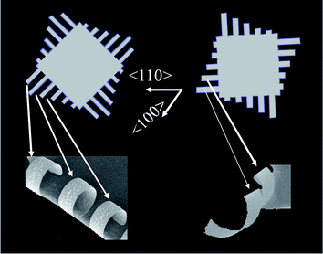 | ||
| Fig. 1 Si/SiGe bilayer cantilever membrane released from patterned substrates. <100>-oriented cantilevers roll into nanorings (left images), while <110>-oriented cantilevers curl into nanocoils (right images), as they prefer to fold along the most compliant <100> direction. The nanorings have a thickness of 60 nm, radius of ∼3.2 μm, and width of 3 μm; the nanocoils have a thickness of 76nm, radius of ∼2.8 μm, and width of 4 μm. Reprinted from ref. 11 with permission. | ||
Another important variable is the relative thicknesses of the two layers making up a bilayer strained membrane. In general, the strain in a bilayer strained membrane can not only relax elastically via bending but also can relax via stretching of the whole film when it is freestanding, depending on the thickness ratio of the two layers.31 The influence of the membrane thickness on bending or stretching of a bilayer can be described as follows. When a compressively strained layer grows on a substrate, its lattice relaxes outward, which applies both a force (stress) and a torque (moment) to the substrate, the former tending to stretch the substrate uniformly and the latter to bend the substrate downward. The magnitude of the force is proportional to the strain and the film thickness (F ∼ εd); the magnitude of torque equals the force (F) times the distance (l) from the mean position of the applied force (middle of the film) to the line of the center of the whole system [middle of the (film + substrate)], as illustrated in Fig. 2. For a thickness much less than that of the substrate, the film applies a relatively small force but a large torque because of a large l, as shown in Fig. 2(a). Consequently, the film bends the substrate without much stretching. The bending increases with increasing film thickness, following the classical Stoney formula,44 but is typically hardly noticeable because the film is generally very thin compared to the substrate. Conversely, for a thickness much greater than that of substrate, the film applies a relatively large force but a small torque because of a very small l, as shown in Fig. 2(c). Consequently, the film stretches the substrate uniformly without much bending. The bending decreases with increasing film thickness, because the torque decreases as force is applied more and more closely to the center of the whole system (diminishing l). When both thicknesses are comparable, the film bends as well as stretches the substrate, as shown in Fig. 2(b). The bending behavior now follows the classical Timoshenko formula.34
 | ||
| Fig. 2 2D schematic illustration of the force (F) and torque (F × l) applied by a compressively strained film (red) grown on a substrate (green) for different film-to-substrate thickness ratios. Reprinted from ref. 31 with permission. | ||
When the elastic properties are isotropic, the bending, rolling, or curling behavior is not so intuitive. It is, however, a situation that can be treated quantitatively. Geometric conditions and shear stress now affect the final membrane morphology. Fig. 3 shows the conditions schematically. If the strained membrane has isotropic elastic properties, it tends to roll into a tube or rug when it is wide or a ring when it is narrow. A long narrow strip may, however, form a coil, as described below, and involves minimization of energy that involves a shear term.
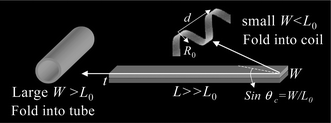 | ||
| Fig. 3 Schematic diagram of rolling or curling a strained bilayer membrane upon release, illustrating the geometric parameters to determine the membrane morphology. The arrows indicate the folding direction. Reprinted from ref. 11 with permission. | ||
The characteristic bending curvature (κ) can be calculated using the Timoshenko formula, shown in eqn (1).31–34 For simplicity, we assume the two layers have the same thickness (t/2) and the same isotropic elastic constants. Then eqn (1) simplifies to κ = −(3εm)/(2t). The bilayer membrane will roll into a tube or ring whose rotations have a characteristic radius R0 = 1/κ and a perimeter length L0 = 2πR0.
 | (1) |
 | (2) |
As the material is elastically isotropic, the membrane is able to curl or roll along all directions that have equal bending energy. But there is also an optimum tube radius, as shown above. When a strained membrane is longer than the perimeter length (L > L0), some extra energy may be associated with it. Any tube that forms can adopt the optimum radius R0 with minimum bending energy only for the first revolution, after which it must adopt a larger radius, thus failing to minimize the total energy. A wide membrane (W > L0) that is being underetched still has no choice but to roll into a tube. There exists a geometric condition to form coils, i.e., W < L0. The strained membrane can roll into a coil by choosing a curling direction having an angle θ with its long edge, so that all the rotations in the coil adopt the optimal radius R0 with the minimum bending energy, but at some cost in shear energy. In contrast, if the membrane rolls into a ring with multiple rotations by curling along its long edge, only its first rotation can adopt R0, while additional rotations must adopt a radius larger than R0, with extra cost of bending energy. From the energy standpoint, a coil can always be favored to form over a tube when W < L0. There is a critical angle θc = sin−1(W/L0) to ensure the membrane rolls into a coil with a certain pitch (d), as shown in Fig. 3. If θ < θc, the membrane rolls into a tube with a continuous tube wall, i.e., “a coil with zero d”. Therefore, there exist two required geometric conditions for coil formation, W < L0, and θ > θc.
The total elastic energy for tube-vs-coil formation can be calculated, in terms of length, width, and thickness of the starting membrane. Fig. 4 shows a phase diagram for a 60nm thick SiGe/Si bilayer membrane, by assuming it has isotropic elastic properties. It defines the geometric regime for tube-vs-coil formation. For a given film length L < L0, tubes dominate no matter how wide the bilayer membrane is, i.e., the minimum length for coil formation is L0. Once L > L0, there exists a critical membrane width above which tubes form and below which coils form. For example, when L/L0 = 10, W/L0 has to be smaller than 0.01 for coil formation; above this value, tube formation is favored. Conversely, for a given membrane width W, there exists a critical length for coil formation L0. Wider membranes (larger W/L0) would require longer membranes (larger L/L0) for coil formation. For example, when W/L0 = 0.02, L/L0 has to be larger than 100 for coil formation; below this value, only tubes form. There exists an upper limit of width, W, for coil formation, 3% of L, as shown in Fig. 4. The phase boundary also depends on the magnitude of membrane elastic properties. Increasing bending modulus or decreasing shear modulus suppresses tube formation and favors coil formation, so that the boundary line in Fig. 4 shifts upward either with increasing bending modulus or decreasing shear modulus.
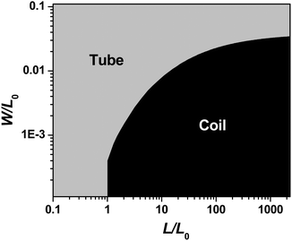 | ||
| Fig. 4 Log-log plot of thermodynamic stability for nanotube or nanocoil formation, as a function of reduced film length L/L0 and reduced width W/L0, for a given set of bending and shear moduli. Here the SiGe/Si bilayer membrane is treated as an isotropic material. Reprinted from ref. 11 with permission. | ||
As mentioned at the start of this section, when elastic anisotropy is introduced, the strained membrane curls only along the most compliant direction, in other words, that factor dominates the energy. The formation of coils is determined by the alignment of the curling direction and the soft direction. The helicity angle, chirality, diameter, and pitch of coils are all width dependent, as shown in Fig. 2 in ref. 48.
A bilayer strained membrane can also wrinkle when released from the holding substrate.29,49–53 In general, wrinkles are caused by the interplay between bending and stretching in the presence of geometric constraints. Fig. 5(a) shows a 3D partially released bilayer strained membrane (L ≫ h), the released portion of which is free to relax elastically.29 There is a constraint, i.e., the boundary condition that no elastic strain relaxation can occur where the membrane is still bonded to the substrate, as shown by the dashed line. The strain gradient and the average strain are defined as Δε = ε1 − ε2 and ![[small epsilon, Greek, macron]](https://www.rsc.org/images/entities/i_char_e0c6.gif) = (ε1t1+ε2t2)/(t1 + t2), respectively, in a bilayer strained membrane.
= (ε1t1+ε2t2)/(t1 + t2), respectively, in a bilayer strained membrane.
 | ||
| Fig. 5 Schematic diagrams of distortions of a strained bilayer membrane with isotropic elastic properties upon release, illustrating the geometric parameters to determine the membrane morphology. (a) Free-hanging bilayer film comprising two layers with thicknesses t1 and t2, subject to biaxial strains ε1 and ε2, respectively. The total length of the bilayer is L. h is the etching length, defined as the distance over which the release layer has been etched away. (b) A bent film with inner radius R, and (c) wrinkled structure with deflection profile ζ(x, y), amplitude A, and wavelength λ. Reprinted from ref. 29 with permission. | ||
We first consider wrinkle formation in elastically anisotropic materials. Again, the membrane will deform only along the most compliant direction. As shown in Fig. 5, if the y direction is the most compliant direction, the bilayer strained membrane will bend and/or stretch freely in the y direction, forming a tube. If the x direction is the most compliant direction, the sheet will attempt to bend and stretch in the x direction, but the constraint causes the formation of wrinkles. This qualitative explanation is valid for single-layer or multilayer membranes. Wrinkling has been demonstrated experimentally,49 as shown in Fig. 6, in an end-constrained single SiGe freestanding layer after release from the host substrate along a trench that is mechanically scratched in the <100> direction, the most compliant direction in SiGe. Three groups of SiGe samples with different Ge composition and thickness were prepared. They all show wrinkles forming in <100> direction after release. The wavelength of wrinkling is measured via atomic force microscopy. The detailed experiment is described in ref. 49.
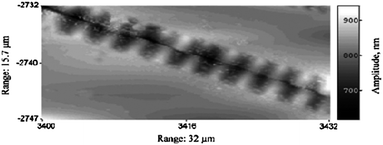 | ||
| Fig. 6 Atomic force microscopy image of a wrinkled freestanding Si0.7Ge0.3 layer. The wrinkles form at both the edges and along the elastically soft <100> directions. Wrinkles are shown as bright regions separated by dark regions. Reprinted from ref. 49 with permission. | ||
Fig. 7 shows that the measured wavelength of wrinkling starts at a certain lateral etching length h for all three groups of samples and then increases with increasing h, (as defined in Fig. 5), indicating there is a critical hc for wrinkle formation. Below hc, the geometric constraint does not allow strain to relax along the trench direction, even though it is the most compliant direction. Energetically, strain could less likely relax along the transverse direction, i.e., the hard <110> direction, so it will be retained mostly in the membrane until h > hc. Wrinkles can only form when h > hc. The wavelength and amplitude of wrinkles as a function of the strain gradient has also been investigated (Fig. 2 in ref. 49). As the strain gradient increases, the wavelength decreases while the amplitude increases. Because the increased strain relaxes preferentially in <100> directions, narrow and high wrinkles form.
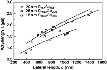 | ||
| Fig. 7 Measured wavelength with respect to the lateral length h, as defined in Fig. 5, for three groups of samples. The solid lines represent the calculated wavelength, Reprinted from ref. 49 with permission. | ||
We now consider strained bilayer membranes with isotropic elastic properties. The strained membrane is able to wrinkle along all directions that have equal bending/stretching energy, if no boundary condition exists. What it does depends on the magnitude of the strain gradient created in it. Qualitatively, if the strain gradient is large, the strained layer must be much thinner than the unstrained layer before releasing the bilayer, to prevent plastic deformation or relaxation and so a large bending moment exists, as shown in Fig. 2(a), which will bend or curl the membrane. Conversely, if the strain gradient is small, the strained layer can be thicker than the unstrained layer, so a large force exists to stretch the bilayer, as shown in Fig. 2(c), leading to wrinkle formation if appropriate boundary conditions exist.
For isotropic elastic properties, again the geometric condition is important for deciding the formation of tubes vs. wrinkles. The etching length (h) determines the released region of the bilayer strained membrane (see Fig. 5). When h is small (L ≫ h), the geometric confinement in the x direction limits relaxation in x; instead strain is relaxed via bending and stretching in the y direction only (unlike the anisotropic case). Increasing h reduces the effect of the constraint in x (it moves the constraint some distance away), and strain can now begin to be relaxed via bending and stretching in both directions. There is no geometric constraint for strain relaxation in the y direction (free boundary condition), while there is a geometric constraint for strain relaxation in x direction (fixed boundary condition). Stretching and/or bending with a constraint leads to wrinkling.29,49–53 There exists a critical etching length for wrinkling, hc. The geometric condition to determine wrinkle formation is h > hc. Large h should allow the bilayer to roll better if the strain gradient is large. A small strain gradient does not provide enough bending moment to roll. If the film cannot roll, it will stretch at the free end, leading to wrinkling (stretching with a constraint) if h is large enough.
The total elastic energy of bent and wrinkled structures has been calculated, in terms of strain gradient, etching length, and layer thickness, for both bilayer11,31–34 and single-layer29,49,53 strained membranes. In this calculation, the membranes are assumed to have isotropic linear elastic properties. The condition to determine bending and wrinkling can be calculated as a function of these variables. For example, Fig. 8 shows a calculated phase diagram29 for a 20nm-thick In0.1Ga0.9As/GaAs bilayer. For small Δε = 0.20% and ![[small epsilon, Greek, macron]](https://www.rsc.org/images/entities/i_char_e0c6.gif) = 0.36%, h0 is calculated as ∼700 nm. The lower-left part of Fig. 8 shows that when h< h0, bending is dominant; when h > h0, wrinkling starts to dominate. To shift bending to wrinkling, one can increase
= 0.36%, h0 is calculated as ∼700 nm. The lower-left part of Fig. 8 shows that when h< h0, bending is dominant; when h > h0, wrinkling starts to dominate. To shift bending to wrinkling, one can increase ![[small epsilon, Greek, macron]](https://www.rsc.org/images/entities/i_char_e0c6.gif) . Fig. 8 shows that by increasing
. Fig. 8 shows that by increasing ![[small epsilon, Greek, macron]](https://www.rsc.org/images/entities/i_char_e0c6.gif) (the dashed line shows 1% tensile strain), the phase boundary shifts upward and wrinkling becomes more dominant (the wrinkling region is enlarged). This can be understood as follows. Large
(the dashed line shows 1% tensile strain), the phase boundary shifts upward and wrinkling becomes more dominant (the wrinkling region is enlarged). This can be understood as follows. Large ![[small epsilon, Greek, macron]](https://www.rsc.org/images/entities/i_char_e0c6.gif) can be achieved by either increasing the strained-layer thickness d2 or decreasing the unstrained-layer thickness d1 by assuming Δε is constant. Doing so will make wrinkling (stretching with constraints) energetically favorable without much bending, as shown in Fig. 5(c). The color bars in Fig. 8 show that in the bending regime, the inner radius of tubes decreases with increasing Δε, while in the wrinkling regime, the wavelength of wrinkles increases with increasing h.
can be achieved by either increasing the strained-layer thickness d2 or decreasing the unstrained-layer thickness d1 by assuming Δε is constant. Doing so will make wrinkling (stretching with constraints) energetically favorable without much bending, as shown in Fig. 5(c). The color bars in Fig. 8 show that in the bending regime, the inner radius of tubes decreases with increasing Δε, while in the wrinkling regime, the wavelength of wrinkles increases with increasing h.
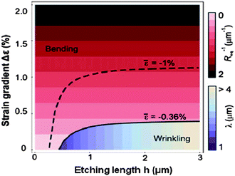 | ||
| Fig. 8 Phase diagram of favorable film shapes based on an energetics comparison between bent and wrinkled structures. Req is the inner radius of the bent structure and λ is the wavelength of the wrinkled structure. Reprinted from ref. 29 with permission. | ||
2.2 Scalability of nanomechanical architectures
A century ago, the bending of a bimetallic strip was analyzed by Timoshenko34 with continuum elasticity theory. The same formula has been applied to model many other materials systems, such as epitaxially grown bilayer thin films.11,31–34 Our design principles for nanomechanical architectures of strained bilayer membranes, strain sharing multilayer membranes, and even membranes made from single materials with a strain gradient, are therefore based on the classical Timoshenko formula.34 However, as the strained membrane gets sufficiently thin, stresses associated with the existence of nearby surfaces become important in the bending, and the classical Timoshenko formula must be modified to account for them.30,35,36,54,55 We discuss these modifications below.Because of the large surface-to-volume ratio, stresses associated with the presence of surfaces are expected to play an important role in determining the bending of nanomembranes. As the membrane gets thinner, the influence of surface related stresses becomes more dominant. The classical Timoshenko formula neglects surface and interface stresses and is therefore valid, in principle, only for relatively thick films for which the surface/interface and the atomic structure can be neglected. As shown in Fig. 9, there exist significant discrepancies between Timoshenko's formula (dashed line) and experimental results (square dots) for very thin membranes.
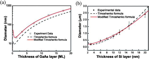 | ||
| Fig. 9 Comparison of results with the classical and modified Timoshenko formulas. (a) Diameters of GaAs/InAs nanotubes as a function of thickness of the GaAs layer with the thickness of the InAs layer fixed at two monolayers (MLs). See ref. 57 for experimental details. (b) Diameters of pure Si micro- and nanotubes as a function of thickness of the Si layer with the thickness of the strained Si layer fixed at 2 nm. See ref. 58 for experimental details. Reprinted from ref. 35 with permission. | ||
Because the surface of most materials is relaxed in some way, either via reconstruction or via chemical modification, one can think of the surface region as a separate phase with its own elastic properties. These are negligible when the nanomembrane is thick, but become important when it is very thin. The properties of this separate phase must be included in the Timoshenko formula. Bending induces an additional surface stress, which equals the product of bending strain and the surface layer elastic constant, namely “surface stress induced by large bending”.35
The Timoshenko formula can be modified to include surface effects. The detailed derivation is described in ref. 35. As an example, Fig. 9(a) plots the diameters of a series of GaAs/InAs nanotubes made with diameters ranging from 20 to 500 nm by varying the thickness of the GaAs layer.57 The dashed line shows smaller diameters predicted by the classical Timoshenko formula. For a GaAs/InAs strained bilayer, the upward bending is induced by the relaxation of misfit strain. When the bilayer is very thin, the surface stress can influence the bending behavior. The intrinsic surface stress of GaAs is, by nature, different from that of InAs due to the surface reconstruction. The differential intrinsic surface stresses between top GaAs and bottom InAs surfaces causes an effect opposite to the bending due to relaxation of misfit strain, causing the radius of curvature to increase. Modifying the classical Timoshenko formula by adding this effect produces a good fit to the data.
The same design principle can be used to scale the diameters of RUNTs made from a single-material membrane. Single-material membranes can, for example, be a membrane of Si in which part of the thickness is strained. This structure can be achieved by growing Si on a Ge layer at a low temperature (300 °C) via molecular beam epitaxy.58 The initial Si layers are strained (although partially relaxed and thus with dislocations), but then begin to relax plastically more fully with increasing film thickness, leading to a strain gradient in the single layer. The detailed fabrication is described in Sec. 3.1. For rolling up single-material strained membranes, α = 1 and eqn (1) reduces to a simpler form
 | (3) |
The diameter of a pure-Si RUNT is estimated by using eqn (3) and compared to experiment, as shown in Fig. 9(b). The classical Timoshenko formula (dashed line) does not fit the data well. Here the surfaces phases on both sides of the nanomembrane are the same and the differential surface stress mentioned above can play no role. But, because the radii of curvature of the inner and outer surfaces are different, the strain induced in the surface phases on each side differs. By adding this effect into eqn (3), the calculation fits the data well.
![Bending of a nanomembrane induced by surface reconstruction. (a) Schematic diagram of the Si(001)-(2 × 1) surface reconstruction, consisting of rows of dimers, which introduce a large surface stress anisotropy. (b)(c) Side views of a six-layer Si film, showing the parallel surface dimer orientations and the balancing surface stress with the dimer bonds on both the top and bottom surfaces. (d) Side view of a five-layer Si film, showing the orthogonal surface dimer orientations and the simulated self bending induced by surface stress imbalance. (e) Conventional picture of a SiGe bilayer film that always bends toward the Si side. (f) Side view of a simulated bent SiGe film demonstrating the increased bending curvature [compared to (e)] as the surface stress acts in concert with the misfit strain. (g) The surface dimers and surface stress configurations are switched as compared to (f), now opposing the misfit strain to induce a bending in the opposite direction. Arrows mark stress directions. Reprinted from ref. 36 with permission.](/image/article/2011/NR/c0nr00648c/c0nr00648c-f10.gif) | ||
| Fig. 10 Bending of a nanomembrane induced by surface reconstruction. (a) Schematic diagram of the Si(001)-(2 × 1) surface reconstruction, consisting of rows of dimers, which introduce a large surface stress anisotropy. (b)(c) Side views of a six-layer Si film, showing the parallel surface dimer orientations and the balancing surface stress with the dimer bonds on both the top and bottom surfaces. (d) Side view of a five-layer Si film, showing the orthogonal surface dimer orientations and the simulated self bending induced by surface stress imbalance. (e) Conventional picture of a SiGe bilayer film that always bends toward the Si side. (f) Side view of a simulated bent SiGe film demonstrating the increased bending curvature [compared to (e)] as the surface stress acts in concert with the misfit strain. (g) The surface dimers and surface stress configurations are switched as compared to (f), now opposing the misfit strain to induce a bending in the opposite direction. Arrows mark stress directions. Reprinted from ref. 36 with permission. | ||
Surface stress caused by reconstruction of the clean surface will act with or against the misfit strain in bending SiGe bilayer membranes, depending on the orientation of surface dimers. Normally, a SiGe membrane bends always towards the Si side, as illustrated in Fig. 10(e). Fig. 10(f) shows surface stress acting with misfit strain to increase the bending toward the Si side, as seen by comparing Fig. 10(e) to Fig. 10(f). However, if we switch the top and bottom surface dimer orientation, as shown in Fig. 10(g), the surface stress will act against misfit strain to decrease the upward bending. For a thin enough membrane or weak lattice mismatch strain the surface stress can be strong enough to reverse the “normal” bending direction defined by misfit strain, making the film bend downward, toward the Ge side.
2.3 Accurate positioning of nanomechanical structures
The position in the surface plane of nanomechanical structures is defined by patterning the corresponding 2D strained membranes via lithographic techniques. Two most common techniques are photo- and electron-beam (e-beam) lithography. Conventional photolithography can be used to pattern many identical structures, suitable for large-scale production. E-beam lithography can be used to pattern individual structures with much smaller dimensions. After patterning, the 2D strained membrane is released from the substrate and rolled up into 3D structures by etching away the underlying sacrificial layer. As mentioned in Sec. 1, the etching rate of the sacrificial layer is one of the extrinsic parameters that defines the desired ultimate 3D structure.Real-time video microscopy reveals that the rolling-up process is highly nonlinear at the beginning, linear at the intermediate stage, and stops for long etching time.9,59 A nonlinear rolling-up process implies a fast mean etch rate, whereas a linear roll-up process would imply a low mean etch rate. Fig. 11 shows a detailed evolutionary view of the process.9 All etching processes start at zero time; the time bar shows the beginning and ending of membrane deformation, respectively, when they are observable.
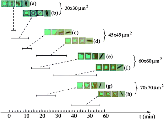 | ||
| Fig. 11 Snapshots of two different etching processes. Fast tube formation from a 30 × 30 μm2 square, a 45 × 45 μm2 square, a 60 × 60 μm2 square, and a 70 × 70 μm2 square are shown in (a), (c), (e), and (g), respectively. Correspondingly, much slower processes are shown in (b), (d), (f), and (h). The time bar shows the beginning and ending of membrane deformation, respectively; when they are observable. The fast process is kinetically controlled and is linearly dependent on the square size. In contrast, the slow process is transport controlled and is nonlinearly dependent on the square size. Reprinted from ref. 9, with permission. | ||
The etching rate has a strong influence on the shape of tubes. Fast etching leads to an asymmetric rolling of tubes while slower etching leads to more symmetric rolling of tubes. When the membrane size is sufficiently large, the degrees of freedom in rolling increase, as well as the possibility of asymmetric rolling,9 as shown in Fig. 11. Moreover, the fast etching process has a linear dependence on the membrane dimension (etching length), which indicates that the mass transport of chemicals is fast enough so that etching is mainly determined by the chemical reaction at the etch front, namely a kinetically controlled etch rate. Conversely, the slow etching process has a nonlinear dependence on the etching length, indicating that the etch rate is transport-controlled. This transport dependence may explain why, in Fig. 11, for the slow processes the 70 × 70 μm2 bar is shorter than the 60 × 60 μm2 one.
Precise positioning of rolled-up tubes can be achieved by controlling the etch rate as well.59 A slow etch rate is the general rule to achieve symmetric rolling of membranes and precise positions of the rolled-up structures over a large area.
3. Fabrication methods
The fabrication of freestanding rolled-up 3D micro- and nano-objects generally consists of three critical steps: (1) the formation of nanometer-thick single- and multilayer strained membranes with defined and generally maximal strain gradient, (2) patterning of the strained membranes into desired geometries, and (3) releasing the patterned membranes from the underlying substrate by selective etching of a sacrificial layer. More specifically, conventional optical lithography and/or e-beam lithography and other nanopatterning techniques can be used to pattern strained membranes into various geometries as well as along different directions. After lithography, the desired patterns are transferred onto strained membranes by using reactive ion etching (RIE). A rinsing/drying step can be added after selective etching. Because they are based on standard device fabrication technology, one can expect the processes to create these rolled-up structures to be highly scalable.3.1. Establishing and tuning strain
Strain modifies the Si band structure by splitting the conduction and valence band valleys or maxima. This band splitting suppresses intervalley scattering and reduces the effective transport mass, resulting in significant carrier mobility enhancement and hence has been used to improve the performance of semiconductor devices and to advance significantly the field of Si-based quantum electronics.60 In contrast, strain relaxation is the driving force behind the rolling-up technology, i.e., formation of 3D nanostructures from 2D patterned sheets. In general, the strain can be created by the following methods: (1) via the lattice mismatch between different crystalline materials with an epitaxial relationship, (2) via non-epitaxial deposition, (3) via differential thermal expansion of two materials, (4) via differential swelling of materials, or (5) in very thin membranes, via differential surface stress, as mentioned in Sec. 2.2.2.We focus on the Group IV materials here. The heteroepitaxial growth of Si/Ge heterostructures is well established. There is a 4% lattice mismatch between Si and Ge. Ideally, one can grow a Ge layer epitaxially onto a Si(001) substrate to create a 4% misfit strain at the Si/Ge interface if the Ge is fully strained. In practice, the strain is so large that the consequences of strain are already evident with the deposition of fraction of a monolayer of the different material. For example, scanning tunneling microscopy (STM) shows the formation of linear defects (misfit dislocations in the surface plane) when pure Ge is deposited on pure Si.74,75 With subsequent growth of pure Ge, coherent 3D nanocrystals form in what is known as the Stranski-Krastanov growth mode76 (initial 2D layer growth, also called the wetting layer, followed by 3D island growth). These 3D nanocrystals can relieve strain because, even though they are coherent with the substrate, their lattice constant can increase vertically, effectively relieving strain. The 3D nanostressors, termed “huts”,1 have four (105) facets whose structure has been thoroughly investigated.1,77Fig. 12 shows a near-atomic-resolution STM image of one such 3D hut, and also shows a cross-section transmission electron microscopy (XTEM) image of the same structure.33
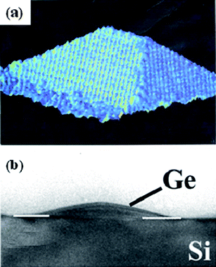 | ||
| Fig. 12 Ge “hut” nanostressor on Si(001). (a) STM image; (b) XTEM image: the white lines show the Ge hut-Si substrate interface. Reprinted from ref. 33 with permission. Images courtesy of Y.-W. Mo and E. Sutter. | ||
In addition to the formation of 3D coherent nanostressor islands as above, a strained film growing on a rigid substrate can reduce built-in strain by a competing mechanism, via dislocation formation, the more conventionally known way. The strain energy tends to be released plastically by dislocations when the strain is relatively small, i.e., for a low-Ge-concentration SiGe alloy on Si(001).78 For films with larger misfit strain, e.g., Ge on Si(001), the system prefers 3D island formation after the 2D-film critical thickness is exceeded, if the temperature is high enough to allow the required diffusion and nucleation kinetics. The nucleation barrier for a 3D coherently strained island79 decreases rapidly with strain as ε−4, while that for dislocations is linear with ε−1. Hence for large strain (high Ge concentration, in this case), 3D island formation is the preferred path to strain energy reduction.
In the creation of strain-engineered nanoarchitectures, we want in general to maximize the strain gradient and to be able to tune the strain to the desired level, which implies that we generally want to avoid unknown plastic strain relaxation, and we generally want a flat film rather than hut formation. Therefore, a practical way to form strained Si/Ge bilayer films is to grow low-Ge-concentration SiGe alloy on a Si(001) substrate, for which the preferential growth is as a 2D layer. The magnitude of misfit strain can be tuned by varying the composition of the SiGe alloy layer, but there are limitations. In order to keep the SiGe alloy layer fully strained, its thickness is always kept below the kinetic critical thickness for the formation of dislocations for that composition.80,81 There are added complications in determining the strain gradient and the maximum strain. Essentially all prior effort has focused on epitaxy on substrates that are much thicker than the growing film, and the models for dislocation formation referenced above relate to that situation. It is only quite recently that systems have been considered in which the substrate is not thick. The way the strain is shared between the growing film and substrate begins to change as the substrate gets thinner. The growing strained film applies effectively an “external” stress to bend and stretch the substrate (Fig. 2). To remain coherent, i.e., not plastically relaxed, the growing film in the conventional system must always be below the critical thickness for dislocation formation, i.e., much thinner than the substrate. When the deposited film is much thinner than the substrate, bending dominates (even though it is ignored because it is so small) and increases linearly with increasing film thickness, following Stoney formula,44 as shown in Fig. 2(a). The behavior when the film thickness becomes comparable to the substrate thickness deviates dramatically from the Stoney formula linear dependence. The behavior now follows the classical Timoshenko formula, as shown in eqn (1) in Sec. 2.1, and can be understood by considering the evolution of strain sharing between the film and substrate (Fig. 2). Strain sharing affects critical thicknesses and defect formation in heteroepitaxy and produces most interesting results in nanoepitaxy.
Using a thin, freestanding substrate allows better strain sharing between growing film and substrate and makes it possible to grow a thicker, fully strained, unrelaxed film on it; whereas the same film grown on a bulk substrate is relaxed via the formation of dislocations. That is so because the thin substrate shares elastically in the strain, by distorting via bending or changing linear dimensions. By doing so, one can maximize the strain gradient and tune the strain to the desired level.
A complication that is not obvious or easily understood works in the opposite direction. If the thin substrate is, in fact, held on a carrier such as the oxide in silicon-on-insulator (SOI) substrate, then it is neither freestanding, nor is the system the same as bulk. The thin substrate in this configuration cannot readily share strain elastically until the oxide is etched and the bilayer structure is released. That has the following consequence: the thermodynamic critical thickness for plastic relaxation actually is lower than for growth of the same layer on a bulk substrate. The reason is that the energy associated with dislocation formation is lower at the oxide/crystalline interface82 and thus the critical thickness is lower. This factor affects the degree of strain one can introduce starting with layered structures such as SOI.
Many possibilities exist for the preparation of substrates for strained-layer Si/Ge growth and subsequent growth. We describe an example. The Si substrate is cleaned with diluted hydrofluoric acid (HF) to etch off the native oxide on the surface, followed with a piranha clean (H2SO4/H2O2) in 10 min, and a diluted HF etch for a few seconds to remove the oxide layer formed during the piranha clean. Epitaxial growth can be most readily achieved via molecular beam epitaxy (MBE) or chemical vapor deposition (CVD), which both provide a precise control of film thickness in the monolayer range. For ultrahigh-vacuum MBE or CVD (UHV-MBE/CVD) growth, the sample is cleaned with an additional 15-minute SC1 clean (NH4OH/H2O2/H2O-mixture) at ∼80 °C and dipped deliberately into diluted HF acid to terminate the surface with hydrogen before transfer to the MBE or CVD chamber, in order to prevent the growth of native oxide. The epitaxial Si/SiGe alloy layer is then grown, for example, onto a Si (001) substrate. The growth temperature is generally ∼600 °C or lower, measured by an optical pyrometer. The Ge composition in the SiGe layer can be varied by changing Ge flux rate in MBE or germane flow rate in CVD, i.e., changing the Ge content in the gas phase. The lower growth temperature prevents the nucleation of dislocations via surface roughening, as surface roughening is thermally activated.78 The composition of SiGe alloy is determined ex-situ by X-ray diffraction. The 2D growth of the strained SiGe layer, or the Si layer on top of that, is monitored in situ with reflection high-energy electron diffraction in UHV by following the diffraction pattern of the (2 × 1) reconstruction. Fig. 13 shows 3D nanostructures83,84 that form from epitaxially grown Si/SiGe bilayer or multilayer membranes after release from the handle substrate.
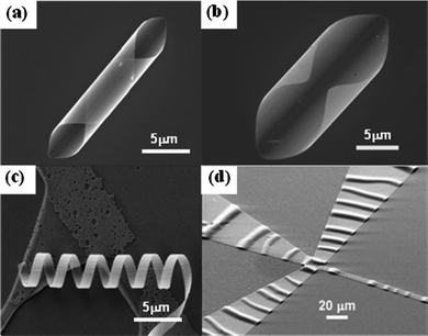 | ||
| Fig. 13 A variety of rolled-up structures fabricated from all-semiconductor strained layers (bilayer and multilayer). (a)–(c) A closed, a partially opened microtube and a microcoil fabricated from Si/Si0.8Ge0.2 (19nm/30nm) (d) Wiggles fabricated from a Si/Si0.8Ge0.2/Si (19nm/30nm/20nm) strained multilayer. Reprinted with permission from ref. 83 and 84. Images courtesy of Minrui Yu. | ||
In Sec. 2 we briefly discussed single-element membranes with a strain gradient that roll up into micro- and nano-objects. We describe the process more fully here. A strain gradient in a Si membrane is created by growing a Ge layer on Si(001) via UHV-MBE at 300 °C.58 The low growth temperature ensures the growth of a smooth, fully plastically relaxed Ge layer. A very thin Si layer is then grown over the Ge. The first few Si monolayers grown on the Ge layer are highly tensilely strained and then, with increasing Si thickness, dislocations start to form in the Si to relax misfit strain. Subsequently deposited Si relaxes further, leading eventually to a fully plastically relaxed Si near the top without relaxing completely the Si deposited first. The result is a tensile-strain gradient in the Si layer with a maximum value at the Si/Ge interface and a minimum value at the outer Si surface (partially/fully relaxed, depending on its thickness). The strain graded Si membrane rolls into a microtube after release from the handle substrate by selectively etching the Ge layer. In this method, the fully plastically relaxed Ge layer is both the stressor layer and the sacrificial layer, providing a unique way to form microtubes. The strain-graded Si contains dislocations.
The Ge condensation technique67,85,86 provides another approach to introduce strain into a membrane system. For example, a 40nm-thick layer of SiGe alloy with uniform Ge composition of 8% is grown on silicon-on-insulator (SOI) with a 27nm-thick template layer and capped with a thin Si layer.67 This Si/SiGe/SOI structure is oxidized at 1050 °C in an oxygen-rich environment. Si in the SiGe alloy is oxidized and Ge is rejected from the alloy and diffuses into the Si template layer of the SOI substrate. The outdiffusion of Ge during the oxidation is prevented by the top SiO2 layer. As a result, the Si template layer becomes SiGe and a gradient of Ge concentration exists in this layer, leading to a compressive-strain gradient in this final SiGe layer on oxide (called SGOI). Both the Ge distribution profile and the Ge content in the SGOI can be tuned by changing the oxidation time. If all Si in SGOI is oxidized, GeOI can be made by using this technique. The membrane will, of course, have dislocations in it. If this SiGe layer is released from the oxide, it will curl because of the strain gradient, just as the Si described in the prior paragraph. It can form into microtubes and wrinkles, depending upon the Ge distribution profile, and the patterning and the length of undercut.28,67Fig. 14 shows microtubes and periodic wrinkles formed by rolling up single-layer strained Si and SiGe films, respectively.
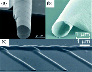 | ||
| Fig. 14 A variety of rolled-up structures fabricated from single-layer strained semiconductor membranes. (a) A 20nm-thick Si tube with diameter of 2 μm, (b) A 10nm- thick SiGe tube with diameter of 1.6 μm. (c) SiGe periodic wrinkles fabricated from SGOI by the Ge condensation technique. Image (a) from ref. 64. Image (b) from ref. 67. Image (c) from ref. 28 with permission. | ||
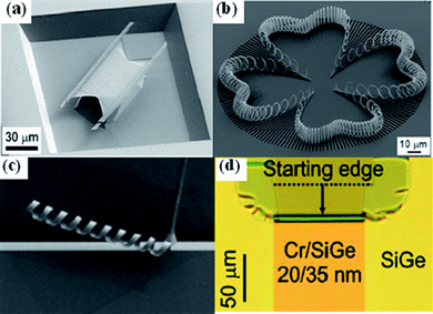 | ||
| Fig. 15 3D structures fabricated from hybrid strained layers. (a) Two suspended Si0.6Ge0.4/Si/Si3N4/Cr (10/10/10/18nm) tubes with the diameter of 3.8 μm. (b) SEM image of ringlike structures formed from a Si/Cr bilayer. (c) A coil formed from a Si0.6Ge0.4/Si/Cr trilayer (11/8/21 nm). (d) A tube formed from a Cr/SiGe bilayer (10/35nm). Image (a) reprinted from ref. 56, images (b) and (c) from ref. 48, and image (d) from ref. 68 with permission. | ||
Metal films have also been incorporated with semiconductor layers to form strained multimaterial nanomembrane structures.12,48,56,68 The metal layer, for instance chromium (Cr), is deposited on top of semiconductor layers by using thermal or e-beam evaporation. The amount of strain created can be controlled by the evaporation rate. A strain gradient can be achieved in metal layers by low-angle glancing deposition. The diameter of micro- and nanotubes or belts formed from hybrid structures can be modeled by the design rules as described in Sec. 2. Fig. 15(c)–(d) show 3D architectures fabricated from hybrid strained layers.
The same principle can be applied to make wavy Si ribbons on flexible polymer substrates87 [e.g., poly(dimethylsiloxane) (PDMS)], as shown in Fig. 16. The CTE of PDMS is approximately two orders of magnitude larger than that of Si. Si membranes can bond to PDMS very well (no delamination even while strained), so the large CTE mismatch between Si and PDMS can cause a large thermally induced strain when the bilayer is heated or cooled. The large strain can shape Si into different forms. This approach has been demonstrated, as shown in Fig. 16(a). First, the Si ribbons are patterned on SOI by photolithography and RIE, and then released in place by underetching the oxide. Second, a PDMS substrate with thickness of 1–3 mm is elastically stretched by heating it to temperatures of between 30 °C and 180 °C. The prestrained PDMS substrate (while it is hot) is bonded with the Si ribbons. The prestrained PDMS is then released by cooling, leading the PDMS to relax back to its unstrained state. This relaxation leads to the spontaneous formation of well-controlled, highly periodic, stretchable wavy structures in Si ribbons. Fig. 16(b) shows wavy Si ribbons with excellent uniformity over a large area and in a highly reproducible fashion.
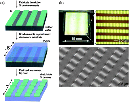 | ||
| Fig. 16 Arrays of wavy Si ribbons on rubber substrates. (a) Schematic illustration of the process for creating wavy Si ribbons on elastomeric substrates (from top to bottom). (b) Top: Optical images of a large-scale aligned array of wavy Si ribbons (widths = 20 μm, spacing = 20 μm, thicknesses = 100 nm) on PDMS. Bottom: SEM image of four wavy Si ribbons from the array shown on top. Images from ref. 87 with permission. Images courtesy of John Rogers. | ||
3.2 Patterning 2D sheets to make rolled-up structures
2D strained layers can be patterned into a variety of geometries as well as along different directions. Many identical structures can be made over a large area, depending on the lithographic techniques. Three general methods are reviewed here. The straightforward method to make patterns is mechanical scratching. Scratching can be simply done using a micrometer sized diamond tip. This method provides a quick check of the rolling behavior of a grown layer system in a short processing time. However, the low controllability of this method makes it difficult to have uniform patterns and smooth edges.Well-controlled patterning is achieved by using either optical or e-beam lithography followed by RIE. The general procedure is as follows: optical/e-beam lithography is used to transfer defined patterns on a photo/e-beam resist film covering the sample surface. Photolithography requires a photomask consisting of a chrome film deposited on a quartz glass. The desired patterns are predefined on it by etching the chrome film. The photomask is inserted between the light source and a resist-covered sample. The patterns are then created on photoresist by exposure and development. The big advantage of photolithography is its high throughput. Many identical patterns can be created over a large area (wafer-level) simultaneously. Light diffraction limits the feature size that can be made by photolithography to optical-wavelength dimensions.
E-beam lithography is used to make features at the nanometer scale by scanning an electron beam across the surface covered by the resist. A predefined mask is not required. E-beam lithography offers flexibility in pattern design and is good for initial characterization of geometric effects on self-rolling. The pattern created in the resist by lithography is then realized in the strained film by using dry etching (RIE). In this process a reactive chemical gas interacts with the surface by using a combination of chemical and physical etching processes. Etch gas atoms are accelerated toward the substrate by a large radio frequency voltage applied in the system and, upon contact, chemically react with the surface while also physically removing material due to their high kinetic energy. RIE is known for its excellent vertical sidewall etching (anisotropic) properties, avoiding the undercut issue in wet etching.
3.3 Selective etching
The fabrication of freestanding rolled-up structures requires releasing the strained membranes from the underlying substrate by selective etching. A sacrificial layer is introduced to facilitate this release. The key factor is the etching selectivity between a sacrificial layer and the membrane. In principle, the sacrificial layer must etch away without etching/damaging the membranes. A high etching selectivity is crucial for a successful release, putting constraints on materials selection.Several release approaches to achieve high etching selectivity to fabricate Group IV semiconductor nanomembranes have been demonstrated. 7–9,11–13,28,48,62–68 Four major approaches are summarized in Table 1 and briefly described here.
• Approach 1: Tubes and coils can be formed from a strained highly boron doped Si/SiGe bilayer with low-doped Si serving as the sacrificial layer.7,12,13 An ammonium hydroxide-water solution (3.7%) is used as the selective etchant because it can etch away low-doped Si at 75 °C,7 8000 times faster than highly doped Si, with boron concentration as high as 1020 cm−3. The etch stop effect is more distinct if a SiGe film is used, because the etching selectivity between Si0.9Ge0.1 and Si is better than 80.62
• Approach 2: Tubes can be rolled up from a strained Si/SiGe layer grown onto a Ge buffer layer, serving as a sacrificial layer.8,58,63 The Ge buffer layer is selectively etched away with 30% H2O2 at room temperature58 or at 90 °C.8 The temperature will determine the differential etch rate, which is critical in the release.
• Approach 3: SiO2 is the most commonly used sacrificial layer for Si membranes. The advantage of using SOI is the very high selectivity of etching between Si and SiO2, in contrast to the use of heavily boron-doped Si or Ge as sacrificial layers. A compressively strained SiGe alloy grows epitaxially on SOI below the kinetic critical thickness for formation of dislocations. The SiGe/Si bilayer would bend or roll naturally downward upon release. This is because compressively strained SiGe would like to expand while tensilely strained Si would like to shrink, resulting in a net downward bending moment, as shown in Fig. 2. The spacing for bending is limited by the thickness of the buried oxide, putting a constraint on the bending process. In order for the SiGe/Si strained bilayer to bend or roll upward upon release from the SOI substrate, an extra thin Si layer is grown on top of the SiGe/Si bilayer to form a Si/SiGe/Si trilayer membrane. The top Si layer has to be thinner than the bottom Si layer to ensure upward bending. The bending curvature decreases (the diameter of tube increases) when the total film thickness increases as predicted by eqn (1) in Sec. 2.1. Alternatively, if one started with SGOI, described in Sec. 3.1.1, tensilely strained Si can be grown on it. The Si/SiGe strained bilayer will bend or roll upward upon release, because an upward bending moment is created (Si grown on SGOI). The advantages of using SGOI over SOI as a substrate is the bending is upward without space limitation and tubes with smaller diameters are possible because the Si/SiGe bilayer is thinner than Si/SiGe/Si trilayer. The drawback is that there are dislocations in SGOI.
• Approach 4: The requirement of high etch selectivity between a sacrificial layer and strained membranes restricts the material choices. Recently, a new approach, using a polymer layer as a sacrificial or template layer, has been developed to overcome this limitation.25,26 As mentioned earlier, most deposited thin films contain stress and a stress (strain) gradient. If such a film (it will be non-single crystal) is deposited onto a polymer sacrificial layer, such as a photoresist, it will contain either compressive or tensile strain. These films will be likely elastically isotropic materials. The strain gradient can be created in single layers or multilayers. In either case, the strained layer, released from the substrate by removing the photoresist (e.g., with acetone), will form micro- or nanotubes or wrinkles, depending on the magnitude of the strain gradient and the geometric conditions (Sec. 2.1).
The uniqueness of this approach is that acetone can remove a polymer layer with 100% selectivity over almost all inorganic materials. The approach makes it possible to roll up a wide spectrum of materials and materials combinations. Moreover, the diameter of microtubes can be tuned by varying the thickness and built-in strain of deposited films. This approach has limitations. Only polycrystalline or amorphous inorganic membranes can be deposited on a polymer layer and they must be deposited at very low substrate temperature to prevent the decomposition of the polymer.
Fig. 17 shows microtubes fabricated via these four major approaches. For all of them, it is clear that the differential etching rate is important. Less clear is that the absolute etching rate is equally important, as the final rolled-up structure is determined by the rate of strain relaxation relative to the absolute etching rate. Several experiments have demonstrated that the rolling process is strongly dependent on the etching rate,9,59,72 as described in Sec. 2.3.
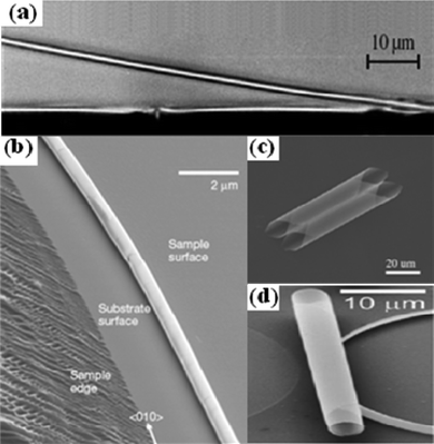 | ||
| Fig. 17 SEM images of tubes formed via different releasing approaches. (a) A highly B-doped Si0.6Ge0.4/Si (20/10nm) tube released via approach 1 described in the text. (b) An undoped Si0.8Ge0.2/Si (6/1nm) tube released via approach 2. (c) Two Si0.8Ge0.2/Si (50/20nm) tubes released from SGOI via approach 3. (d) A SiO2/SiO tube released from a polymer sacrificial layer via approach 4. Image (a) from ref. 61. Image (b) from ref. 8. Image (c) from ref. 9. Image (d) from ref. 26 with permission. | ||
3.4 Large-scale fabrication
Large-scale fabrication of identical strained-membrane nanomechanical architectures not only depends on the intrinsic geometric and physical conditions as described in Sec. 2, but also relies on extrinsic processing parameters as described in Secs. 3.1 and 3.2. In order to fabricate many identical nanoarchitectures simultaneously, a controllable and reliable fabrication process is required.9,72 The nanomechanical-architecture approach is compatible with standard device fabrication technology. Strained nanomembranes are created via CVD growth with a precise control of film uniformity. Conventional lithography is performed to pattern the strained membrane into many identical patterns, which are then realized by RIE. Release is performed with selecting etching. Etching uniformity is necessary to obtain consistent tube or other structure formation over a large area. Uniform etching over a large area can be achieved in a controlled wet-etching process. Fig. 18 shows arrays of Si/SiGe microtubes that have been made in parallel by following the procedure described here. The large-area fabrication of InAs/GaAs nanotubes has also been demonstrated.72 Uniform-etching processes are described in ref. 9 and 72. | ||
| Fig. 18 An array of 270 tubes rolled up from SiGe/Si bilayer squares (30μm × 30μm) by underetching of SiO2 in HF solution for 13.2 min. Snapshots at 20 s, 10 min, and 13.2 min are shown in (a), (b), and (c), respectively. Reprinted from ref. 9 with permission. | ||
4. Properties of membrane-based 3D nanoarchitectures
The nanomechanical architectures described in Secs. 2 and 3 combine the excellent properties of their constitutive materials with their unique 3D geometry, with significant implications for their use as electro- and optomechanical sensors, and in electronic, optoelectronic, and nanofluidic applications. In this scenario a detailed knowledge of structural, mechanical, electronic, optical, and surface properties of rolled-up films is a prerequisite.A significant effort has indeed been made in the characterization of various kinds of rolled-up structures. Detailed structural characterization of tube walls, performed by scanning and transmission electron microscopy (SEM/TEM) reveals that semiconductor membranes rolled into tubes with diameters in the micro- and sub-micrometer range preserve their single-crystal nature, and that defects form in a tube only where the rolling of the membrane involves misorientation.39,42,59,61 Good structural stability of various rolled-up objects (i.e., tubes, rings, and spirals) subjected to mechanical12,13,90 and thermal stresses17,42 has been reported. Electrical conductivity in a bent membrane has been measured and proven to be in the same range as for a flat film.17 The magnetotransport in electron systems formed in curved membranes has been investigated.15,65,91 Visible photoluminescence (PL) has been observed at room temperature from Si nanostructures embedded in a cylindrical solid matrix.16,20,92 The intensity of the PL signal acquired from rolled-up films, including Si nanostructures, is of the same order of magnitude. Rolled-up tubes can act as optical ring resonators, because of their circular cross-section.16 More recently, optical wave guiding in Si/SiOx tubes has also been demonstrated.92 A novel radiation emission mechanism has been proposed in wrinkled SiGe/SiGe membranes.93 A local-wetting induced deformation of SiGe/Si curled membranes has been demonstrated. This deformation suggests that distinctive far-field radiation patterns in the terahertz (THz) range could be achieved.84 In this section, we briefly review the results that lead to the conclusions listed above.
4.1 Structural properties
A detailed study of the wall structure of rolled-up tubes has been reported for all-semiconductor and hybrid structures. Scanning and transmission electron microscopy (SEM/TEM), electron energy loss and secondary-ion mass spectroscopy (EELS and SIMS), as well as micro-Raman spectroscopy, have been performed for this purpose. This section focuses on characterization of all-semiconductor group-IV structures.In early work,61 high-resolution TEM (HRTEM) was performed to demonstrate the single-crystalline structure of a Si0.2Ge0.8/Si/Si0.2Ge0.8 trilayer rolled-up tube with an inner diameter of 10 nm. Fig. 19 shows TEM images of a portion of the tube freestanding over the edge of the substrate. A HRTEM image of the tube wall [Fig. 19(b)] clearly shows the single-crystal structure of the bent trilayer with {111} atomic planes spaced by 3.1 Å. Recent advances in TEM sample preparation have allowed cross-sectional TEM (XTEM) of rolled-up tubes and investigation of the elemental distribution across the tube wall by spatially resolved EELS.16,39,59 This technique has been employed to demonstrate that the walls of the rolled-up tubes formed by multiple rotations of the semiconductor membranes alternate crystalline semiconductor and thin amorphous-oxide layers. A detailed description of the fabrication process and of the characterization of this structure is reported in ref. 16.
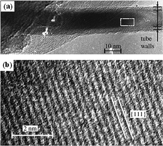 | ||
| Fig. 19 TEM images of a freestanding rolled-up tube. (a) Plane-view HRTEM image of a 1nm Si0.2Ge0.8/1nm Si/0.5nm Si0.2Ge0.8 tube with a diameter of 10nm. (b) Zoomed-in image of the area denoted by the rectangle in (a). Reprinted from ref. 61 with permission. | ||
The prospect of integrating Group IV based tubes with mainstream Si electronics to make lab-on-chip devices requires considering the structural stability of rolled-up layers at high annealing temperatures. The thermal stability of B doped Si0.67Ge0.33/Si tubes was investigated via local laser heating combined with SEM and Raman spectroscopy.42 Approach 1 described in Sec. 3.3 for releasing the bilayer was used. The TEM image and selected-area electron diffraction pattern reveal the good crystal quality of a single freestanding tube.39 SIMS profiles indicate that uniform B doping with a concentration of ∼1 × 1020 cm−3 exists in a 9nm/Si0.67Ge0.33/17 nm Si bilayer. The wall thickness measured by SEM (17nm) was thinner than the value derived from SIMS data (∼26nm), as shown in Fig. 1 in ref. 42. This discrepancy was attributed to an insufficient etching selectivity. As a result, the bilayer was partially etched during the release processing, which led to a lower wall thickness, demonstrating that high etching selectivity is crucial for a controlled release with predictable outcomes.
Fig. 20 shows the Si0.67Ge0.33/Si tube collapses after local laser annealing at an excitation power of 6.7 mW for 5 min. Raman spectroscopy is used to measure the vibrations of chemical bonds in materials. Heating a material causes a change in vibration frequency and a Raman peak shift and so Raman spectroscopy can be used to characterize the thermal stability of tubes.42Fig. 21 shows Raman spectra as a function of excitation power and corresponding tube wall temperature. The laser annealing is performed in air. At low excitation power (≤ 0.7 mW), the measured Raman spectra are dominated clearly by separated peaks related to the vibration modes of the Si–Si bond in the Si and SiGe layers of the tube wall. There is no observable shift of the Si–Si peak at the low excitation power, indicating that no significant heating of the tube occurs. A tensile-strain gradient in the Si layer of the tube wall causes the Si–Si peak of the Si layer to broaden and shift to 517 cm−1, relative to the peak of Si–Si bonds in the unstrained substrate at 520 cm−1.
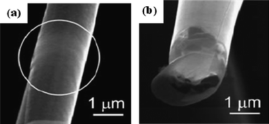 | ||
| Fig. 20 SEM images of single freestanding tube rolled from a 9nm-Si0.67Ge0.33/17-nm Si bilayer, before (a) and after (b) annealing at 6.7 mW for 5 min. The circle in (a) indicates the local annealed region. Reprinted from ref. 42 with permission. | ||
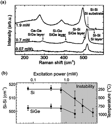 | ||
| Fig. 21 Raman spectra of a single freestanding 9 nm Si0.67Ge0.33/17 nm Si tube. (a) Raman spectra at excitation power ranging from 0.07 to 1.9 mW. (b) Raman shifts of Si–Si vibration mode in the Si and SiGe layers, respectively, as a function of excitation power and corresponding tube wall temperature. Reprinted from ref. 42 with permission. | ||
When the excitation power is increased to 1.9 mW or above, heating causes the Si–Si peaks from the Si and SiGe layers to shift toward lower wave numbers. These two Si–Si peaks merge at high excitation power. The Si-Ge and Ge-Ge peaks in the SiGe layer become more pronounced after heating, indicating the tube structure is changed because of interdiffusion of Si and Ge, and due to Ge condensation in the annealed area. The tube wall structure starts to become unstable. Fig. 21(b) shows the temperature corresponding to an excitation power of 6.7 mW is 925 °C, i.e., a temperature high enough to promote a significant Si-Ge interdiffusion and Ge condensation in the tube wall. The tube is then broken after heating at a high temperature for several minutes, as shown in Fig. 20. The trend of degradation of the tube structure, according to the shifts of Si–Si peaks caused by thermal heating, is summarized in Fig. 21(b). The detailed Raman spectroscopy is described in ref. 42.
4.2 Mechanical properties
The excellent mechanical strength of a Si/SiGe microspiral was demonstrated qualitatively in early work.61 It can be bent through an angle > 900 and can be significantly stretched along its axial direction without fracture.61 This behaviour indicates the microspiral is extremely elastic. A quantitative study of mechanical properties of a nanocoil and a nanobelt has been performed recently via the micromanipulation technique.12,13,90 We briefly describe the mechanical characterization here.The strained membranes roll into 3D nanostructures after release from the substrate. The rolled-up structures rest on or are still attached to the substrate. They can be cut off and picked up by a manipulator, for example, a sharp tungsten (W) probe, and soldered to an AFM cantilever using e-beam induced deposition in the SEM chamber, as shown in Fig. 22(a) and (b). A micromanipulator installed in a SEM chamber, equipped with an atomic force microscope (AFM) cantilever, allows in situ monitoring of the manipulation process.
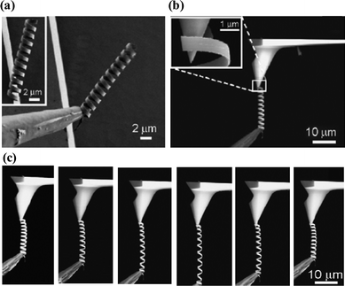 | ||
| Fig. 22 SEM images for picking up and manipulation processes of a nanocoil created from the 11 nm SiGe/8 nm Si/21 nm Cr trilayer. (a and b) An as-fabricated nanocoil (inset of a) is picked up by a W probe and soldered to the tip of an AFM cantilever. Inset to (b) is an enlarged image. (c) Stiffness characterization via stretching and relaxing the nanocoil between the W tip and AFM cantilever (from left to right). All images have the same 10 μm scale bar. Reprinted from ref. 12 with permission. | ||
The detailed soldering process can be found in ref. 12. By moving the W tip downward (upward), the nanocoil is elastically stretched (contracted). The applied force is measured by the AFM cantilever and the deformation of the nanocoil is recorded by SEM. The mechanical properties of a nanocoil rolled from a 11 nm SiGe/8 nm Si/21 nm Cr multilayer have been investigated with such an experimental setup.12Fig. 22(c) shows a series of SEM images of the manipulation process. The durability of the nanocoil is tested by repeating the pulling process for several cycles. No damage to the nanocoil is observed. The elongation length with respect to applied force reveals that a linear relationship between applied force and elongation exists until the spring is extended to 91% of its original length, indicating the excellent elasticity of the nanocoil. A spring constant of 0.003 N/m for this nanocoil is obtained by linear fitting of experimental data.12 This spring constant is an order of magnitude smaller than that of the most flexible available AFM cantilever (∼10−2 N/m). Such nanocoils are expected to be useful as ultrasensitive force sensors.
The radial stiffness of a multiwalled Si/Cr nanoring has also been investigated using the same method.13 The enlarged SEM image in Fig. 23 shows no plastic deformation and sliding between interlayers, indicating the multi-walled nanoring remains closed during the pulling process. The elongation with respect to external load is plotted in Fig. 23. The spring constant of a 2.5-turn Si/Cr (35/10nm) nanoring is determined as 0.332 N/m by linear fitting of experimental data. The stiffness of the nanoring is tunable by varying the number of rotations (wall thickness) and the ring width.
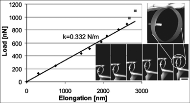 | ||
| Fig. 23 Radial stiffness characterizations of single 35 nm Si/10 nm Cr nanobelts. Inset shows a series of SEM images for pulling the nanoring from left to right with increasing external load. Zoomed-in image of the nanoring denoted in the circle shows no fracture occurs during the pulling. Reprinted from ref. 13 with permission. Image courtesy of Li Zhang. | ||
Another interesting study tests the interlayer bonding strength of a multi-walled nanoring by unrolling it using a manipulator probe.90 SEM measurements reveal that the adjacent interlayers of a Si/Cr multi-walled nanoring are bonded, forming a closed ring. The strong interlayer bonding can be attributed to hydrogen bonds formed between bilayers, originating from the wet selective etching generally used in the releasing process.90
4.3 Electrical properties
The first electrical characterization of a rolled-up structure was performed in 2001.61 The results showed a resistance of 10 kΩ for a highly boron doped 124 nm-thick rolled-up SiGe/Si microspiral with a diameter of 13 μm.61 In this work, the microspiral was detached by a manipulator from the Si substrate after release and transferred onto a new substrate with two metal contacts. Very recently, a novel device has been designed to integrate a freestanding microtube with two metal contacts, which facilitates a comprehensive electrical characterization of a freestanding microtube.17Fig. 24 shows a device layout and SEM images of a freestanding tube connected to two contacts. The strained Si0.64Ge0.36/Si bilayer was highly boron doped (Si0.64Ge0.36:B/Si:B). It rolled into a tube after etching off the sacrificial layer (lightly doped Si) via Approach 1 described in Sec. 3.3. The SEM images in Fig. 24 show a typical 10nm Si0.64Ge0.36:B/8nm Si:B tube bridged over the substrate surface between the two designated contacts. A 10nm Ti/200nm Au film was evaporated in the contact areas for the Si:B/SiGe:B bilayer, forming ohmic contacts, which is crucial for a two-probe measurement.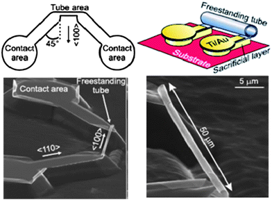 | ||
| Fig. 24 A device with a freestanding SiGe/Si tube connected to two contacts. Upper panel: A mask design for a tube bridged between two contacts and a schematic diagram of the device after etching the sacrificial layer; bottom panel: SEM images of a freestanding tube rolled from a Si0.64Ge0.36:B/Si:B bilayer bridging two contacts. Reprinted from ref. 17 with permission. | ||
The electrical characterization is performed by applying a voltage and measuring the current between the contacts. The current–voltage (I–V) characteristic was measured for three different cases as shown in Fig. 25: before (dash-double dotted line) and after (solid line) rolling up a 10 nm Si0.64Ge0.36/8 nm Si bilayer, and after the complete lift-off of the bilayer from the substrate (dashed line). Fig. 25 shows that the I–V curve is linear in the whole range, both for the unreleased film and the rolled-up tube, a characteristic of ohmic contacts. The grey area represents the error bar (±3%) obtained for the I–V curve of the rolled-up film by measuring fifteen tubes. The inset shows that the maximum current passing from one contact to the other through the substrate is about two orders of magnitude lower than the one measured prior to the complete release of the tube. The resistances (Rasg) of the unreleased film and a rolled-up tube are 10 and 22 kΩ, respectively, and the corresponding sheet resistances are 0.2 and 0.44 kΩ/square, respectively. These values are in fairly good agreement with the calculated values. The calculated sheet resistance for the unreleased bilayer with doping level N = 1.7 × 1020 cm−3 is 0.33 kΩ/square, which corresponds to a resistance of 14 kΩ for the designed pattern. An increase of sheet resistance of the film after release from the substrate is observed. This may be explained by the influence of charging in surface states on the conductance. A high density of surface states that act as charge traps may be generated on the inner and outer surfaces of the tube wall, which are covered with a thin chemical oxide. A surface depletion layer grows with the surface charges, leading to a decrease of the effective conducting region of the tube wall.17
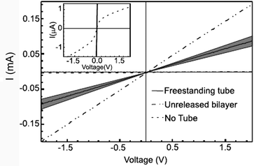 | ||
| Fig. 25 I–V curves measured for a Si0.64Ge0.36:B/Si:B bilayer between the two contacts before the etching of the sacrificial layer: Rasg = 10 kΩ (dash-double dotted line) and after it, for a freestanding tube: Rasg = 22 kΩ (solid line) and in the case that the bilayer is completely lifted off (dashed line). The inset is a magnification of the I–V curve recorded after the removal of the tube from the substrate. Reprinted from ref. 17 with permission. | ||
The tube resistance with respect to the thickness of the SiGe/Si bilayer was also investigated. The dependence of the tube resistance on the bilayer thickness shows a monotonic decrease, from 110 kΩ for the thinnest film (15 nm) to 9 kΩ for a 30-nm-thick layer. The tube resistance can be decrease further after rapid thermal annealing at a moderate temperature (∼700 °C). The details of the measurement with respect to the tube thickness and annealing are described in ref. 17.
Electron transport in low-dimensional electron systems with respect to the magnetic field (magnetotransport) has been characterized in rolled-up III–V membranes.15,71 The results show that magnetotransport in freestanding curved/tubular membranes after release is quite different from that in its planar counterpart, still attached to the underlying substrate. The magnetoresistance in the nonplanar membranes is higher than in the planar ones at zero magnetic field and then increases further with applied magnetic field, but in a manner similar to the planar one.71 The initial rise may be attributed to an increase of electron scattering by surfaces. There exist dangling bonds at the bottom (inner) surface of tubular membranes after releasing from the host substrate by etching away the sacrificial layer. They may act as surface scattering centers and affect the electrical properties. The top surface is assumed to be the same as that of flat ones.
The magnetotransport in nonplanar SiGe/Si membranes has been investigated as well.91 In this work, the low-temperature ballistic magnetoconductance is calculated in a curved SiGe/Si resonant quantum cavity (RQC) under a low bias. Fig. 1 in ref. 91 shows a sketch of a curved 300 x300 nm2 RQC created on a SiGe/Si bilayer membrane with a flat bottom tethered to the substrate. Narrow (∼50nm) quantum point contacts connect the cavity to the source and drain leads. The 2D electron system is formed at the interface between the strained undoped Si and the relaxed n-type doped SiGe. The detailed calculation can be found in ref. 91. The influence of curvature on electric transport with/without the magnetic field is calculated.
Fig. 4 in ref. 91 shows that the conductance (G0 = 2e/h) is very sensitive to the curvature (α) variation at a given sheet carrier density (N = 4 × 1010 cm−2). In zero/low magnetic field, at lower curvatures, the carrier density is high at the drain-end quantum contacts, meaning there is a current flow between the source and the drain. As curvature increases, the coupling between the source and the drain decreases, reducing the conductance. The conductance can be modulated by changing the curvature while in the high magnetic field as well.91
4.4 Optical properties
Rolled-up tubes as building blocks for optical devices were proposed for the first time in 2006.15 The functionality of III–V based tubes was demonstrated via ring resonators and optical waveguides. In these early works, optical modes circulating in the tube cavity (i.e., whispering-gallery modes), and propagating along the tube axis were probed by the photoluminescence from low-density InAs quantum dots embedded in the tube wall. The same concept (i.e., incorporating an optically active material as an internal light source in the circular cavity) was applied to demonstrate the optical functionality of group IV based tubes.16,92 In both these studies, annealing of Si/SiOx tubes is used to fabricate Si nanostructures integrated into a rolled-up solid-state matrix. The detailed description of the fabrication process can be found in ref. 16.The Si/SiOx tubes undergo rapid thermal annealing at 850 °C for 30 min to activate a Si/SiO2 phase separation in the Si-rich oxide, leading to the formation of Si agglomerates in the tube wall. The optical properties of a hybrid Si/SiOx microtube have been investigated using fluorescence and microphotoluminesence (μ-PL) spectroscopy. SEM and XTEM images, shown in Fig. 26, demonstrate that 7 nm SiOx/8nm Si bilayers can roll into microtubes with multiple rotations, resulting in the formation of a radial SiOx/Si superlattice in the tube wall. The XTEM image [Fig. 26(b)-top panel] shows the tube wall structure after the thermal-annealing step. The SiOx/Si superlattice remains intact and a sharp SiOx/Si interface is observed. Energy filtered TEM (EFTEM) is performed to reveal the oxygen content in the amorphous regions [see Fig. 26(b) bottom panel].
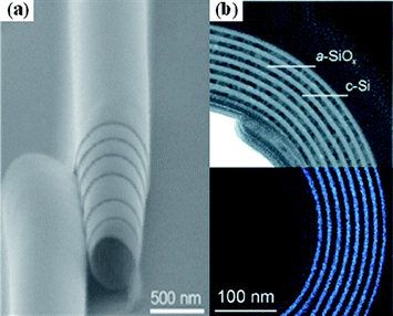 | ||
| Fig. 26 A typical rolled-up tube from 7 nm SiOx/8 nm Si. (a) SEM image. (b) XTEM image of a tube wall consisting of 7 nm a-SiOx (bright area) and 8 nm c-Si (dark area). False-color EFTEM of the Si/SiOx tubewall illustrates the oxide content in the SiOx layer. Reprinted from ref. 16 with permission. Image courtesy of Oliver Schmidt. | ||
μ-PL spectroscopy is performed on SiOx/Si rolled-up tubes at both 8 K and room temperature. A laser operating at 532 nm with a spot size of ∼2 μm was used as a light source. A modulation of the PL spectrum appears in freestanding SiOx/Si tubes because of optical resonant modes occurring inside the tube wall as a certain wavelength of light circulates in the tube. The PL spectra at 8 K in Fig. 27 show that pronounced modes with different spacing depend on the tube diameter. The mode spacing is inversely proportional to the diameter of the resonator. Following the discussion in ref. 16, finite domain time difference (FDTD) simulations were performed to obtain both the optical resonant energies and the intensity pattern from the rolled-up tube structures. Modes are labeled according to their azimuthal (M) and radial (N) numbers. The refractive index of the SiOx area is assumed as a constant value equal to 1.7. The refractive index of the Si area is varied as a function of wavelength. The simulated results are in good agreement with the experiment. Fig. 27 presents the intensity pattern of a mode at an energy of 1.95 eV (M = 20 and N = 1). This pattern reveals that the light can be confined inside the tube wall despite its small thickness (40 nm). Nevertheless, the limited tube wall thickness is probably the main reason for the linewidth broadening of the resonant modes. Based on FDTD simulations, it is expected that by increasing the number of rotations, the light losses can be reduced, leading to an improvement of the quality factor of the structure and a narrowing of the mode peaks.
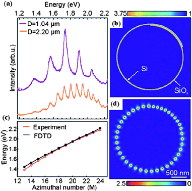 | ||
| Fig. 27 PL spectra at 8 K of a single freestanding SiOx/Si microtube with diameters of 1.04 μm (upper spectrum) and 2.2 μm (lower spectrum). (b) Refractive-index contrast of the rolled-up tube used for the FDTD simulations. The tube wall consists of 20 nm SiOx/20 nm Si.(c) Energy positions of the modes extracted from the lower spectrum in (a) compared to the mode energies as a function of the azimuthal number (M) obtained from FDTD simulation. (d) Intensity pattern of the resonant mode at 1.95 eV with M = 20 and N = 1 from the structure shown in (b). Reprinted from ref. 16 with permission. | ||
Waveguiding along the axis of annealed Si/SiOx tubes has also recently been demonstrated.92 Microtubes rolled from a 20 nm Si/5 nm SiOx bilayer are investigated. The Si/SiOx tubes undergo the previously described annealing process to promote formation of emitting Si nanoclusters in the tube wall. Tubes lying on the substrate or transferred onto a quartz plate are excited using a laser with wavelength of 532 nm focused to a 4 μm spot by a 20x microscope objective. The emitted light is collected through the same objective and detected with a spectrometer equipped with a Si charge-coupled-device (CCD) camera. To study light emission and propagation along its whole length, the rolled-up tube is aligned with the entrance slit of the spectrometer. In this way the tube is imaged on the CCD camera, enabling spatially resolved spectroscopy. Motorized linear stages allow the tube to be translated with respect to the laser spot in the direction parallel and perpendicular to its axis.
Fig. 28 (a)–(c) displays PL spectra collected at the photoexcited region and at the tube exits when the laser beam is focused near the bottom end of a 80 μm-long tube with a ∼2 μm diameter [see inset in Fig. 28(b)]. The modulation of the broad PL spectrum observed in Fig. 28(b) is caused by the resonant optical modes confined in the tube wall. Because modes are caused by constructive interference of light confined in a section of the tube, no modulation is observed for light propagating along the tube axis and escaping from the tube ends [Fig. 28(a) and (c)]. The spectra collected from those regions are red-shifted with respect to the spectrum collected from the region where the laser spot is focused. The measured red shift is attributed to light re-absorption in delocalized states of the nanostructured Si, more pronounced at shorter-wavelength mode peaks. The asymmetry of the wide band emitted at the photoexcited point drastically changes for the PL signal acquired at the tube exits, as shown in Fig. 28.
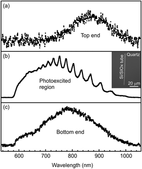 | ||
| Fig. 28 PL spectra acquired from the top end (a), the photo excited region (b), and the bottom end (c) of a 80 μm-long tube with laser beam focused near the bottom end. The inset in (b) is an optical image of a typical tube on quartz. Reprinted from ref. 92 with permission. | ||
Conventionally, optical emission from semiconductors is via the conduction-to-valence band optical transitions. Very recently, a novel radiation emission mechanism from wrinkled Si1−xGex/Si1−yGey membranes has begun to be explored.93 The emission mechanism is based on the change of acceleration of carriers, when they travel along the sinusoidal trajectory in wrinkled Si1−xGex/Si1−yGey membranes, a manner similar to synchrotron radiation with undulators, or like a free-electron laser. As shown in Fig. 29, as a voltage is applied across the periodically wrinkled structure, the carriers (holes in p-type Si1−xGex/Si1−yGey wrinkled structures) change direction periodically. The acceleration of carriers will change correspondingly, resulting in emission of radiation. The same effect is expected to occur in n-type wrinkled membranes.
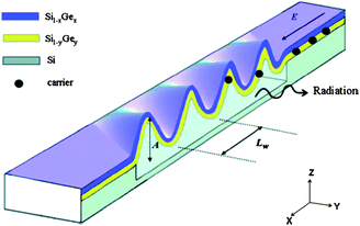 | ||
| Fig. 29 Schematic illustration of a wrinkled structure. A voltage applied across the wrinkled structure leads to carriers (solid dots) moving in the wrinkled bilayer though a sinusoidal path. Reprinted from ref. 93 with permission. | ||
The theoretical analysis demonstrates that the emission wavelength covers a wide spectrum, depending upon the periodicity of wrinkles (Lw) and the velocity of holes in response to the electric field (E). The velocity of carriers is proportional to the magnitude of electric field, i.e., v = μE, where μ is the mobility. Fig. 30 shows the emission wavelength (λ′) as function of E for different Lw. λ′ decreases as E increases and/or Lw decreases. The mobility is set to 1400 cm2 V−1 s−1. The detailed calculation is described in ref. 93. The calculated radiation power in the infrared (IR) range is in the order of milliwatts for a p-type Si0.51Ge0.49/Si0.82Ge0.18 wrinkled structure with Lw of 0.1 μm. An optimal Lw can be designed based on the design principles described in Sec. 2. Periodically wrinkled membranes may be the realization of a real-space undulator, and can serve as an electromechanically tunable broadband electromagnetic frequency source (the Blick–Lagally oscillator).94
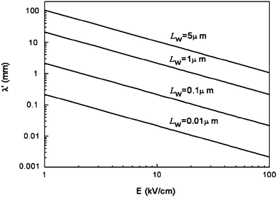 | ||
| Fig. 30 Emission spectra with respect to the wrinkle periodicity and the electrical field. Reprinted from ref. 93 with permission. | ||
4.5 Surface properties
Thinness, a unique feature of nanomembranes, creates a large surface-to-volume ratio. Nanomembranes are mechanically ultra-compliant as well, which make them sensitive to very small external forces. One can expect that modification of membrane surfaces may lead to the deformation of membranes. Very recently, local-wetting induced deformation of rolled-up SiGe/Si membranes has been demonstrated.84 The SiGe/Si membranes are patterned and aligned to the <100> crystalline orientation (the most compliant direction in SiGe/Si). The Si layer is epitaxially grown on SGOI to form the bilayer membrane and it is released from its host substrate via Approach 3 described in Sec 3. By careful control of the rate and uniformity of etching, a large array of freestanding 3D tubes can be achieved, as shown in Fig. 18.As shown in Fig. 13 (a) and (b), two different tube shapes can be obtained by careful design of membrane patterns. The partially opened tubes are used to study the surface chemical modification of curved membranes. Acetone, dyed green, is chosen to modify the surface properties. A small amount of acetone is dropped on the partially opened tube. As acetone evaporates the surface tension on the tube surfaces changes correspondingly. The differing evaporation rates of acetone from top (Si) and bottom (SiGe) surfaces of the tube causes an imbalance in surface tension, leading to a net force to open the tube. The opening process is recorded via video microscopy. Fig. 31(a)–(d) shows micrographs of time sequences of tube opening and recovery as acetone evaporates from its surfaces. The evaporation rate of acetone inside the tube can be represented as a wetting length (L). Fig. 31(e) shows that the opening gap of the tube does not increase until five seconds and reaches a maximum value in six seconds, and then decrease to its initial gap, as L decreases with time. The detailed description can be found in ref. 84.
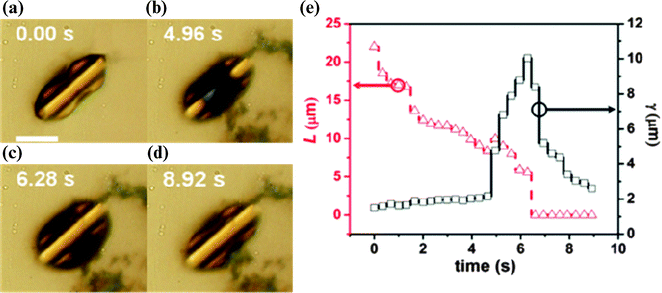 | ||
| Fig. 31 Time-lapse sequences of a tube being opened and then recovering due to acetone evaporation on its surface. (a)–(d) Optical images. (e) Temporal changes of wetting length L (left axis) and the opening gap γ (right axis). Scale bar is 10 μm. Reprinted from ref. 84 with permission. Images courtesy of Minrui Yu. | ||
5. Potential applications of rolled-up and wrinkled membranes
In Secs. 2 and 3, we described the design principles and fabrication techniques to roll up semiconductor and composite membranes into a variety of 3D nanostructures. In order to provide a backdrop for potential applications, we discussed materials properties in Sec. 4. In this section, we briefly enumerate some of the most promising applications.5.1 Microfluidics for biomedical applications
A promising application of rolled-up microtubes is as microfluidic channels.15,18 The microtubes constrain the flow of liquids. Fluorescence measurements were performed to observe the liquid spread in the tubes. 15,18 Because Si-based tubes are more readily integrated with modern Si technology, one can, in principle, position the microfluidic channel near electronic sensing circuits that can be used, for example, to count the flow of charged molecules through the tubes. Furthermore, the tubes may be envisioned as possible drug delivery systems in living organisms. Tubes can be made in quite small size by engineering the strain and film thickness of strained layers based on the design principles described in Sec. 2. Tubes with small diameter (<20 nm) can potentially be used for nanoinjection needles, nozzles for inkjet printing, and small-quantity fluid dispensers.5.2 Ultrasensitive force sensors
Rolled-up nanosprings can have a very small spring constant,12 at least an order of magnitude smaller than that of the most flexible available AFM cantilever (∼10−2 N/m), as described in Sec. 4.2. Hence nanosprings are capable of sensing very small force with high accuracy and can be used as ultra-small force nanosensors/nanoactuators. The radial stiffness of a multiwalled Si/Cr nanoring has also been measured. For example, the spring constant of a 2.5-turn Si/Cr (35/10nm) nanoring is determined as 0.332 N/m.13 The stiffness of a nanoring is tunable by varying the number of rotations (wall thickness) and the ring width, so nanorings may be usable as compact extended-range pressure sensors.5.3 Current-driven swinging micromirrors
A micromirror device has been fabricated by release of a SiGe/Si epitaxial bilayer from the underlying SOI substrate.95 The micromirror is supported by curved hinges. A gold conductive layer is deposited onto the bilayer for electrical characterization before the release step. The mechanical swinging of the micromirror is demonstrated by passing a current through it. Net angular displacements larger than 10 degrees are obtained at voltages smaller than 2V. The performance characteristics of these micromirrors are comparable to or better than the reported values for other MEMS optical switches or beam scanning devices.5.4 On-chip refractometric sensors
Rolled-up Si/SiOx miocrotubes can be used as refractometers.20 A Si/SiOx microtube acts both as a natural pipe and as an optical sensor. Refractometry was tested by inserting a sugar solution into the microtube, leading to a change in refractive index and resulting in a shift of resonant-mode peak positions. μ-PL spectroscopy using a laser was employed to characterize the microtube's optical response. Integrated PL intensity mapping was performed by scanning the laser over the microtube in submicron steps before and after the sugar solution was introduced into the microtube. These results reveal that spatial regions can be identified by air and solution modes, respectively. Comparing experimental data with simulations shows that the spectral sensitivity of this refractometer is remarkable. 205.5 Semiconductor optical emitter
Emission of radiation from periodic wrinkled Si1−xGex/Si1−yGey bilayer membranes has been proposed.93,94 When carriers move through a periodically wrinkled structure, the acceleration of carriers will change correspondingly, resulting in emission of radiation. The radiation frequency can cover a wide spectral range depending on the wavelength of wrinkles and velocity of carriers. A radiation power of mWs in the IR region is predicted for a microdevice containing a two-dimensional electron gas with a wrinkle wavelength of 0.1 μm.5.6 Remote chemical sensors
A partially opened Si/SiGe tube is mechanically very flexible, making it sensitive to tiny external-load changes on its surface. Such tubes can be used as chemical sensors if molecules selectively adsorb/desorb to/from the Si/SiGe bilayer and cause an elastic deformation of the tube.84 Chemically functionalizing one side of the membrane can enhance selectivity.5.7 Advanced antenna architectures
High-frequency lightweight antennas are needed for wireless communications ranging from consumer electronics to defense and space applications. Increasing the operating frequency of antennas from the MHz range into the THz range reduces signal loss and enhances efficiency. Conventionally, a metal coil fabricated by bending a metal strip is used for making antennas. A THz antenna requires the diameter of coil to be at the nanometer scale. Nanocoils created by rolling up nanomembrane strips are potential candidates for making THz antenna. Simulations reveal that nanocoil antennas can be operated at THz frequencies.96,97 The operating frequency can be tuned by varying the geometric parameters of nanocoils, such as the diameter, spacing, and number of turns. These parameters can be precisely controlled by the film thickness, length, and built-in strain. Nanocoil fabrication is compatible with standard semiconductor technology, making it is possible to fabricate antennas and other components of communication devices simultaneously and define their positions precisely.6. Conclusions
In this review we retraced the successful story of strain-driven nanoarchitectures with a particular focus on group IV semiconductors. Templated self-assembly of nm-thick membranes into 3D objects combines top-down semiconductor processing and strain-driven actuation to fold 2D membranes into predictable shapes (e.g., tubes, helices, corner cubes, and periodic wrinkles) and configurations (e.g., wrinkled channel networks) on a substrate surface.An additional value to the approach reviewed in the previous sections comes from the uniqueness of the result, i.e., nanostructures that combine the excellent properties of their constitutive materials (e.g., semiconductors or hybrid multilayer stacks) with their 3D geometry and ordered arrangement. Indeed, the work done in the past 10 years has demonstrated that the excellent structural, mechanical, electronic, optical, and surface properties of semiconductor thin films are not confined to planar configurations, but are preserved to a large extent in a 3D shaped membrane. The crystal structure of nanomembranes has proved to be unaffected by out-of-plane deformation for Si tubes with diameters of a few hundred nanometers or less, and good structural stability of various rolled-up objects (i.e., tubes, rings, and spirals) under mechanical and thermal stresses has been reported. These are significant results in the perspective of fabricating electronic, mechatronic, or photonic devices onto a 2D template before release from the substrate surface.
The hollow geometry of many of the nanomechanical architectures described in this review makes them ideal candidates for micro- and nanofluidics, optical ring resonators, and high-frequency radiation emitters. Both rolled-up tubes and periodic wrinkles are highly scalable in size, enabling a high tunability of resonator, emitter, or microfluidic-device response. The flexibility of nanomembranes also allows dynamic or post-processing changes of a 3D device response, even quite locally.
There is a message from the work of the last 10 years on nanoarchitectures. A century after Timoshenko analyzed the bending of bimetallic strips, fabrication of nanomechanical architectures has grown into a well established technology, yielding device structures with unique functionalities. Future research in this field may involve the integration of 3D devices implementing different functionalities on the same substrate and eventually on a transferable flexible support. Starting with 2D nanomembranes as a platform, the self-assembly into 3D nano-objects in a controllable manner paves the way for exploring many potential additional applications of inorganic nanomembranes based on single-crystal semiconductors.
Acknowledgements
Work described in this review that was performed at the University of Wisconsin-Madison was supported by US DOE (Grant No. DE-FG02-03ER46028), by US NSF/MRSEC Program (DMR-0520527), and by US AFOSR (FA9550-09-1-0230). Work described in this review that was performed at the University of Utah was supported by US DOE (Grants No. DE-FG02-03E46027 and DE-FG02-04ER46148). Preparation of this review was supported by AFOSR-MURI (Grant #FA9550-08-1-0337). The authors would like to thank R. Blick and D. Savage for helpful discussions and thank M. Yu, Y.-W. Mo, E. Sutter, L. Zhang, O. Schmidt, and J. Rogers for the use of images.References
- Y.-W. Mo, D. E. Savage, B. S. Swartzentruber and M. G. Lagally, Phys. Rev. Lett., 1990, 65, 1020 CrossRef CAS.
- R. Nötzel, Semicond. Sci. Technol., 1996, 11, 1365 CrossRef.
- K. Hiruma, M. Yazawa, K. Haraguchi, K. Ogawa, T. Katsuyama, M. Koguchi and H. Kakibayashi, J. Appl. Phys., 1993, 74, 3162 CrossRef CAS.
- C. Thelander, P. Agarwal, S. Brongersma, J. Eymery, L. F. Feiner, A. Forchel, M. Scheffler, W. Riess, B. J. Ohlsson, U. Gösele and L. Samuelson, Mater. Today, 2006, 9, 28 CrossRef CAS.
- S. Iijima, Nature, 1993, 354, 56.
- H. Engelkamp, S. Middelbeek and R. J. M. Nolte, Science, 1999, 284, 785 CrossRef CAS.
- V. Ya. Prinz, V. A. Seleznev, A. K. Gutakovsky, A. V. Chehovskiy, V. V. Preobrazhenskii, M. A. Putyato and T. A. Gavrilova, Phys. E., 2000, 6, 828 CrossRef CAS.
- O. G. Schmidt and K. Eberl, Nature, 2001, 410, 168 CrossRef CAS.
- H. Qin, N. Shaji, N. E. Merrill, H. S. Kim, R. C. Toonen, R. H. Blick, M. M. Roberts, D. E. Savage, M. G. Lagally and G. Celler, New J. Phys., 2005, 7, 241 CrossRef.
- X. Li, J. Phys. D: Appl. Phys., 2008, 41, 193001 CrossRef.
- M. Huang, C. Boone, M. Roberts, D. E. Savage, M. G. Lagally, N. Shaji, H. Qin, R. H. Blick, J. A. Nairn and F. Liu, Adv. Mater., 2005, 17, 2860 CrossRef CAS.
- L. Dong, L. Zhang, D. J. Bell, D. Grützmacher and B. J. Nelson, J. Phys. Conf. Ser., 2007, 61, 257 CrossRef.
- D. Grützmacher, L. Zhang, L. Dong, D. J. Bell, B. J. Nelson, A. Prinz and E. Ruh, Microelectron. J., 2008, 39, 478 CrossRef.
- T. Kipp, H. Welsch, Ch. Strelow, Ch. Heyn and D. Heitmann, Phys. Rev. Lett., 2006, 96, 077403 CrossRef CAS.
- S. Mendach, R. Songmuang, A. Rastelli, M. Benyoucef and O. G. Schmidt, Appl. Phys. Lett., 2006, 88, 212113 CrossRef.
- R. Songmuang, A. Rastelli, S. Mendach and O. G. Schmidt, Appl. Phys. Lett., 2007, 90, 091905 CrossRef.
- F. Cavallo, R. Songmuang and O. G. Schmidt, Appl. Phys. Lett., 2008, 93, 143113 CrossRef; P. Zhang, E. Tevaarwerk, B.-N. Park, D. E. Savage, G. K. Celler, I. Knezevic, P. G. Evans, M. A. Eriksson and M. G. Lagally, Nature, 2006, 439, 703 CrossRef; S. A. Scott, W. Peng, A. M. Kiefer, H. Jiang, I. Knezevic, D. E. Savage, M. A. Eriksson and M. G. Lagally, ACS Nano, 2009, 3, 1683 CrossRef CAS.
- A. A. Solovev, Y. F. Mei, E. Bermúdez Ureña, G. S. Huang and O. G. Schmidt, Small, 2009, 5, 1688 CrossRef CAS.
- G. S. Huang, Y. F. Mei, D. J. Thurmer, E. Coric and O. G. Schmidt, Lab Chip, 2009, 9, 263 RSC.
- A. Bernardi, S. Kiravittaya, A. Rastelli, R. Songmuang, D. J. Thurmer, M. Benyoucef and O. G. Schmidt, Appl. Phys. Lett., 2008, 93, 094106 CrossRef.
- Y. Forterre, J. M. Skotheim, J. Dumais and L. Mahadevan, Nature, 2005, 433, 421 CrossRef CAS.
- R. Abermann, Thin Solid Films, 1984, 115, 185 CrossRef CAS.
- J. A. Thornton, Thin Solid Films, 1989, 171, 5 CrossRef.
- F. Elstner, C. Gautier, O. Piot, G. Contoux, F. Cosset, F. Nardou and J. Machet, Phys. Status Solidi A, 1996, 154, 669 CrossRef.
- Y. F. Mei, G. S. Huang, A. A. Solovev, E. Bermúdez Ureña, I. Moench, F. Ding, T. Reindl, R. K. Y. Fu, P. K. Chu and O. G. Schmidt, Adv. Mater., 2008, 20, 4085 CrossRef CAS.
- V. Luchnikov, O. Sydorenko and M. Stamm, Adv. Mater., 2005, 17, 1177 CrossRef CAS.
- Ch. Deneke, R. Songmuang, N. Y. Jin-Phillipp and O. G. Schmidt, J. Phys. D: Appl. Phys., 2009, 42, 103001 CrossRef.
- Y. Mei, D. J. Thurmer, F. Cavallo, S. Kiravittaya and O. G. Schmidt, Adv. Mater., 2007, 19, 2124 CrossRef CAS.
- P. Cendula, S. Kiravittaya, Y. F. Mei, C. Deneke and O. G. Schmidt, Phys. Rev. B: Condens. Matter Mater. Phys., 2009, 79, 085429 CrossRef.
- F. Liu, M. G. Lagally and J. Zang, MRS Bull., 2009, 34, 190 CAS.
- M. Huang, P. Rugheimer, M. G. Lagally and Feng Liu, Phys. Rev. B: Condens. Matter Mater. Phys., 2005, 72, 085450 CrossRef.
- F. Liu, P. Rugheimer, E. Mateeva, D. E. Savage and M. G. Lagally, Nature, 2002, 416, 498 CrossRef CAS.
- F. Liu, M. Huang, P. Rugheimer, D. E. Savage and M. G. Lagally, Phys. Rev. Lett., 2002, 89, 136101 CrossRef.
- S. Timoshenko, J. Opt. Soc. Am., 1925, 11, 233 Search PubMed.
- J. Zang and F. Liu, Appl. Phys. Lett., 2008, 92, 021905 CrossRef.
- J. Zang, M. Huang and F. Liu, Phys. Rev. Lett., 2007, 98, 146102 CrossRef.
- A. Cho, Science, 2006, 313, 164 CrossRef CAS.
- A. Malachias, C. Deneke, B. Krause, C. Mocuta, S. Kiravittaya, T. H. Metzger and O. G. Schmidt, Phys. Rev. B: Condens. Matter Mater. Phys., 2009, 79, 035301 CrossRef.
- N. Y. Jin-Philipp, J. Thomas, T. Kelsch, R. Songmuang, Ch. Deneke and O. G. Schmidt, Appl. Phys. Lett., 2006, 88, 033113 CrossRef.
- S. Mendach, S. Kiravittaya, A. Rastelli, M. Benyoucef, R. Songmuang and O. G. Schmidt, Phys. Rev. B: Condens. Matter Mater. Phys., 2008, 78, 035317 CrossRef.
- D. J. Thurmer, C. Deneke, Y. Mei and O. G. Schmidt, Appl. Phys. Lett., 2006, 89, 223507 CrossRef.
- R. Songmuang, N. Y. Jin-Phillipp, S. Mendach and O. G. Schmidt, Appl. Phys. Lett., 2006, 88, 021913 CrossRef.
- Y. F. Mei, S. Kiravittaya, M. Benyoucef, D. J. Thurmer, T. Zander, C. Deneke, F. Cavallo, A. Rastelli and O. G. Schmidt, Nano Lett., 2007, 7, 1676 CrossRef CAS.
- G. G. Stoney, Proc. R. Soc. London, Ser. A, 1909, 82(553), 172–178 CAS.
- J. J. Wortman and R. A. Evans, J. Appl. Phys., 1965, 36, 153 CrossRef CAS.
- P. G. Evans, D. S. Tinberg, M. M. Roberts, M. G. Lagally, Y. Xiao, B. Lai and Z. Cai, Appl. Phys. Lett., 2005, 87, 073112 CrossRef.
- H.-J. Kim-Lee, D. E. Savage, C. S. Ritz, M. G. Lagally and K. T. Turner, Phys. Rev. Lett., 2009, 102, 226103 CrossRef.
- L. Zhang, E. Ruh, D. Grützmacher, L. Ding, D. J. Bell, B. J. Nelson and C. Schönenberger, Nano Lett., 2006, 6, 1311 CrossRef CAS.
- A. I. Fedorchenko, A.-B. Wang, V. I. Mashanov, W.-P. Huang and H. H. Cheng, Appl. Phys. Lett., 2006, 89, 043119 CrossRef.
- W.-P. Huang, H. H. Cheng, A. I. Fedorchenko and A.-B. Wang, Appl. Phys. Lett., 2007, 91, 053103 CrossRef.
- R. Huang and Z. Suo, J. Appl. Phys., 2002, 91, 1135 CrossRef CAS.
- V. Ya. Prinz, V. A. Seleznev, A. V. Prinz and A. V. Kopylov, Sci. Technol. Adv. Mater., 2009, 10, 034502 CrossRef.
- E. Cerda and L. Mahadevan, Phys. Rev. Lett., 2003, 90, 074302 CrossRef CAS.
- J. Zang and F. Liu, Nanotechnology, 2007, 18, 405501 CrossRef.
- D. Yu and F. Liu, Nano Lett., 2007, 7, 3046 CrossRef CAS.
- S. V. Golod, V. Ya. Prinz, P. Wagli, L. Zhang, O. Kirfel, E. Deckhardt, F. Glaus, C. David and D. Grützmacher, Appl. Phys. Lett., 2004, 84, 3391 CrossRef CAS.
- Ch. Deneke, C. Muller, N. Y. Jin-Phllipp and O. G. Schmidt, Semicond. Sci. Technol., 2002, 17, 1278 CrossRef CAS.
- R. Songmuang, Ch. Deneke and O. G. Schmidt, Appl. Phys. Lett., 2006, 89, 223109 CrossRef.
- Ch. Deneke and O. G. Schmidt, Phys. E., 2004, 23, 269 CrossRef CAS.
- N. Shaji, C. B. Simmons, M. Thalakulam, L. J. Klein, H. Qin, H. Luo, D. E. Savage, M. G. Lagally, A. J. Rimberg, R. Joynt, M. Friesen, R. H. Blick, S. N. Coppersmith and M. A. Eriksson, Nat. Phys., 2008, 4, 540 CrossRef CAS.
- S. V. Golod, V. Ya Prinz, V. I. Mashanov and A. K. Gutakovshy, Semicond. Sci. Technol., 2001, 16, 181 CrossRef CAS.
- F. Wang, Y. Shi, J. Liu, Y. Lu, S. Gu and Y. Zhang, J. Electrochem. Soc., 1997, 144, L37 CrossRef CAS.
- O. G. Schmidt and N. Y. Jin-Phillipp, Appl. Phys. Lett., 2001, 78, 3310 CrossRef CAS.
- L. Zhang, E. Deckhardt, A. Weber, C. Schönenberger and D. Grützmacher, Nanotechnology, 2005, 16, 655 CrossRef CAS.
- L. Zhang, E. Deckardt, A. Weber, C. Schönenberger and D. Grützmacher, Microelectron. Eng., 2006, 83, 1233 CrossRef CAS.
- A. Vorob'ev, P. O. Vaccaro, K. Kubota, T. Aida, T. Tokuda, T. Hyayshi, Y. Sakano, J. Ohta and M. Nunoshita, J. Phys. D: Appl. Phys., 2003, 36, L67 CrossRef CAS.
- F. Cavallo, R. Songmuang, C. Ulrich and O. G. Schmidt, Appl. Phys. Lett., 2007, 90, 193120 CrossRef.
- F. Cavallo, W. Sigle and O. G. Schmidt, J. Appl. Phys., 2008, 103, 116103 CrossRef.
- P. O. Vaccaro, K. Kubota and T. Aida, Appl. Phys. Lett., 2001, 78, 2852 CrossRef CAS.
- Ch. Deneke and O. G. Schmidt, Phys. E., 2004, 23, 269–273 CrossRef CAS.
- N. Shaji, H. Qin, L. J. Klein, C. Deneke, O. G. Schmidt and R. H. Blick, Appl. Phys. Lett., 2007, 90, 042101 CrossRef.
- I. S. Chun and X. Li, IEEE Trans. Nanotechnol., 2008, 7(4), 493 CrossRef.
- J. Q. Hu, Y. Bando, J. H. Zhan, M. Y. Liao, D. Golberg, X. L. Yuan and T. Sekiguchi, Appl. Phys. Lett., 2005, 87, 113107 CrossRef.
- X. Chen, Z. Y. Zhang and M. G. Lagally, Phys. Rev. Lett., 1994, 73, 850 CrossRef CAS.
- F. Wu, X. Chen, Z. Y. Zhang and M. G. Lagally, Phys. Rev. Lett., 1995, 74, 574 CrossRef CAS.
- I. N. Stranski and V. L. Krastanov, Abhandlungen der Mathematisch-Naturwissenschaftlichen Klasse. Sitzungsberichte der Akademie der Wissenschaften in Wien, Math.-naturwiss. Kl. IIb, 1939, 146, 797 Search PubMed.
- Y. Fujikawa, K. Akiyama, T. Nagao, T. Sakuri, M. G. Lagally, T. Hashimoto, Y. Morikawa and K. Terakura, Phys. Rev. Lett., 2002, 88, 176101 CrossRef CAS.
- F. K. LeGoues, B. S. Meyerson, J. F. Morar and P. D. Kirchner, J. Appl. Phys., 1992, 71, 4230 CrossRef CAS.
- J. Tersoff and F. K. LeGoues, Phys. Rev. Lett., 1994, 72, 3570 CrossRef CAS.
- J. W. Matthews and A. E. Blakeslee, J. Cryst. Growth, 1974, 27, 118 CAS.
- D. C. Houghton, J. Appl. Phys., 1991, 70, 2136 CrossRef CAS.
- C. Euaruksakul, M. M. Kelly, B. Yang, D. E. Savage, M. G. Lagally and G. K. Celler, ACS Nano Search PubMed , submitted.
- Y. Zhang, M. Yu, D. E. Savage, M. G. Lagally, R. H. Blick and F. Liu, Appl. Phys. Lett., 2010, 96, 111904 CrossRef.
- M. Yu, M. Huang, D. E. Savage, M. G. Lagally and R. H. Blick, IEEE Trans. Nanotechnol., 2010 DOI:10.1109/TNANO.2010.2066986.
- T. Tezuka, N. Sugiyama and S. Takagi, Appl. Phys. Lett., 2001, 79, 1798 CrossRef CAS.
- S. Nakaharai, T. Tezuka, N. Sugiyama, Y. Moriyama and S. Takagi, Appl. Phys. Lett., 2003, 83, 3516 CrossRef CAS.
- D. Khang, H. Jiang, Y. Huang and J. A. Rogers, Science, 2006, 311, 208 CrossRef CAS.
- S. Tanaka, C. C. Umbach, J. M. Blakely, R. M. Tromp and M. Mankos, Appl. Phys. Lett., 1996, 69, 1235 CrossRef CAS.
- V. Zielasek, F. Liu, Y. Zhao, J. B. Maxson and M. G. Lagally, Phys. Rev. B: Condens. Matter Mater. Phys., 2001, 64, 201320 CrossRef.
- L. Zhang, L. Dong and B. J. Nelson, Appl. Phys. Lett., 2008, 92, 143110 CrossRef.
- G. J. Meyer, N. L. Dias, R. Blick and I. Knezevic, IEEE Trans. Nanotechnol., 2007, 6, 446 CrossRef.
- F. Cavallo, R. Songmuang, A. Rastelli, M. Benyoucef and O. G. Schmidt, Proceedings of the IV Conference of Group IV Photonics, San Francisco, 9–11 Sept 2009 Search PubMed.
- A. I. Fedorchenko, H. H. Cheng, G. Sun and R. A. Soref, Appl. Phys. Lett., 2010, 96, 113104 CrossRef.
- R. Blick and M. G. Lagally, patent applied for, 2007.
- T. Tokuda, Y. Sakano, D. Mori, J. Ohta, M. Nunoshita, P. O. Vaccaro, A. Vorob'ev, Kubota and N. Saito, Electron. Lett., 2004, 40, 1333 CrossRef CAS.
- Y. M. Senousy, E. V. Moiseva and C. K. Harnett, University Government Industry Micro/Nano Symposium (UGIM), Louisville, KY, July 200813–16 Search PubMed.
- M. Yu and R. H. Blick, private communication.
| This journal is © The Royal Society of Chemistry 2011 |
