Nanostructure of buried interface layers in TiO2 anatase thin films grown on LaAlO3 and SrTiO3 substrates
Regina
Ciancio
*a,
Elvio
Carlino
a,
Carmela
Aruta
b,
Davide
Maccariello
b,
Fabio Miletto
Granozio
b and
Umberto
Scotti di Uccio
b
aCNR-IOM TASC, Area Science Park, Basovizza S.S. 14 Km 163.5, 34149, Trieste, Italy. E-mail: ciancio@tasc.infm.it
bCNR-SPIN and Dipartimento di Scienze Fisiche, Complesso Universitario di Monte SantAngelo,
Via Cintia, I-80126, Napoli, Italy
First published on 24th October 2011
Abstract
TiO2 anatase thin films grown by pulsed laser deposition are investigated by high resolution transmission electron microscopy and high angle annular dark field scanning transmission electron microscopy. The analyses provide evidence of a peculiar growth mode of anatase on LaAlO3 and SrTiO3 characterized by the formation of an epitaxial layer at the film/substrate interface, due to cationic diffusion from the substrate into the film region. Pure TiO2 anatase growth occurs in both specimens above a critical thickness of about 20 nm. The microstructural and chemical characterization of the samples is presented and discussed in the framework of oxide interface engineering.
One of the most exciting developments of modern condensed-matter physics has been the recent discovery of a wide spectrum of functional behaviors in complex oxide heterostructures.1,2 The recent technological advancements in producing oxide thin films with a high degree of crystal perfection and the capability to tailor the electronic structure of their interfaces have propelled these systems towards new perspectives of device applications and technology. In this context, semiconductor heterostructures have represented the birthplace of fascinating discoveries both in fundamental research as well as for potential applications in nanoscale photonics and electronics. Among them, the binary oxide TiO2 is a key material for the wide spectrum of applications including photocatalytic, catalytic and optical devices, gas and humidity sensors, optoelectronic and spintronic devices.3–5 In all the cases, highly textured thin films of TiO2 are required and a crucial role is played by the interface properties. For instance, it has been observed that crystalline defects and poor interfacial quality may cause spin-flips in ferromagnetic TiO2 films, thus reducing the spin polarization value.2 Since a well defined interface is known to have an impact on both microstructures and properties of the deposited films, a precise control of the crystalline quality and of the nature of the film/substrate interface is mandatory both to optimize the performances of TiO2-based devices and to investigate fundamental processes in this material.
TiO2 most commonly exists in three polymorphs: anatase, rutile and brookite, the rutile phase being thermodynamically favored at high temperature. Nevertheless, epitaxial growth of anatase is sometimes preferred due to the higher photocatalytic activity with respect to the rutile phase. TiO2 anatase thin films have been grown by several deposition techniques2,6–11 and on a wide variety of oxide substrates. In particular, the perovskites (001)LaAlO3 (LAO) and (001)SrTiO3 (STO) have low lattice mismatch (0.26% and 3.1%, respectively) with the anatase tetragonal cell (a = 0.378 nm and c = 0.952 nm) allowing epitaxy with a high level of crystal perfection.2,9–11
In spite of the considerable effort of the scientific community, the heteroepitaxial growth of TiO2 thin films, usually pursued by molecular beam epitaxy and sputtering techniques, has not been completely optimized to date.2 An exhaustive understanding of the chemical assessment of the anatase/substrate interfaces is also lacking. To date, a few works report on TiO2 anatase growth by pulsed laser deposition (PLD), although this technique allows growing very high quality thin films and heterostructures.2
In this communication, we show that interphase epilayers easily form at the film/substrate interface when TiO2 is deposited on LAO and STO by PLD under usual growth conditions. Such interphase epilayers are related to the intrinsic thermal reactivity of TiO2 with the LAO and STO perovskite substrates. By resorting to cross-sectional high resolution transmission electron microscopy (HRTEM) and high angle annular dark field (HAADF) scanning TEM (STEM) analyses, we determine the nanostructure of the TiO2 films and of the interfaces with the substrates and derive conclusions on the role of atomic interdiffusion in TiO2 anatase samples grown on (001) LAO and TiO2-terminated STO substrates. The samples were deposited by pulsed laser deposition (KrF excimer laser, 248 nm) with fluence 2 J cm−2 at the target, 700 °C substrate temperature and 10−1 mbar oxygen pressure, at a rate of about 0.02 nm s−1 and monitored in situ by reflection high energy electron diffraction (RHEED). The TEM/STEM analyses were carried out using a JEOL 2010 UHR field emission gun microscope operated at 200 kV with a measured spherical aberration coefficient Cs of 0.47 ± 0.01 mm. Hence, the relevant interpretable resolution limit in HRTEM is 0.19 nm.12 The microscope is equipped with an Oxford system for energy dispersive X-ray spectroscopy (EDS) studies. HAADF images were acquired using an illumination angle of 12 mrad and a collection angle 88 ≤ 2θ ≤ 234 mrad. The setup for the STEM dark field experiments produces images whose contrast is approximately proportional to the square of the average atomic number of the illuminated area and to the thickness of the specimen foil.17EDS analyses were carried out in STEM mode by scanning an electron probe of 0.5 nm to precisely determine the elemental chemical profiles across the interfacial region. Cross-sectional samples in the [010] zone axis suitable for TEM/STEM analyses have been obtained by a conventional polishing technique followed by dimpling and ion milling. The ion mill process was performed following a well-established protocol to avoid preferential sputtering at the substrate/film interface.13
Fig. 1 is the RHEED pattern acquired at the end of the film deposition on a LAO substrate which shows the expected 4 × 1 reconstruction and a good surface quality. Similar results have been obtained also for the film grown on a STO substrate.
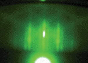 | ||
| Fig. 1 RHEED pattern at the end of the deposition of a 40 nm thick TiO2 film on LAO substrate. | ||
A representative overview of the TiO2/LAO cross-sectional region is given in the bright field image of Fig. 2(a) obtained under multi-beam conditions with the primary electron beam parallel to the [010] crystal direction of the film. The film is about 40 nm thick and has a typical domain structure with a domain size ranging from 20 to 100 nm (two domain's boundaries are pointed by arrows in Fig. 2(a)). As shown in Fig. 2(a), the film is made of two adjacent slabs (henceforth called L1 and L2), each about 20 nm thick, running parallel to the [100] LAO crystallographic direction. Diffractograms recorded over several areas of the two regions reveal no differences between the Bravais lattice of L1 and L2, both being compatible with the anatase polytype. The [010] zone axis HRTEM image in Fig. 2(b) shows the characteristic modulated structure of the film due to the occurrence of crystallographic shear planes.14HRTEM investigation shows that the interface region is atomically flat and, differently from previous works,9,10 no secondary phases are present in the film nanostructure. The film and the substrate have a (001)(010)TiO2//(001)(010)LAO orientation relationship, as highlighted by the diffractogram displayed in Fig. 2(c) related to the region in Fig. 2(b). To better understand the origin of the diffraction contrast variation between the two regions of the film, HAADF and EDS experiments have been performed. A representative HAADF image of the LAO/L1/L2 region is shown in Fig. 2(d). Because of the strong difference in the average atomic number between LAO and TiO2, the HAADF signal saturates over the substrate region (bright saturated contrast region in Fig. 2(d)) when ideal detection conditions are achieved for imaging the film. Image contrast variations are seen between the L1 and the L2 region indicating possible chemistry differences between them, the brighter contrast of L1 being characteristic of a higher average atomic number. EDS elemental profiles collected across the L2/L1 region (dash edged box in Fig. 2(d)) reveal indeed the occurrence of Al diffusion from the substrate into the L1 region, as displayed in Fig. 2(e). The results from the HAADF and EDS experiments along with the crystallographic evidence indicate that, under the deposition conditions, the Al diffusion occurs over the first 20 nm of the film leaving the crystal structure unchanged. Since, as enlightened by HAADF contrast, the area affected by Al diffusion has a higher average atomic number with respect to pure TiO2, we can conclude that the diffusing Al ions are most likely allocated at the interstitial sites of the anatase structure to stabilize the formation of oxygen vacancies. These findings are also supported by theoretical calculations.15
![(a) Bright field TEM image of the TiO2/LAO film in the [010] zone axis showing the splitting of the film into adjacent regions (L1 and L2) with different diffraction contrast. The arrows point two crystal domain boundaries; (b) HRTEM image in the [010] zone axis of the TiO2/LAO interfacial region; (c) diffractrogram of the TiO2/LAO interfacial region; (d) HAADF/STEM image of the TiO2/LAO interfacial region. The dash-edged box indicates the area where the EDS map of aluminium distribution has been acquired; (e) EDS elemental profile of Al.](/image/article/2012/NR/c1nr11015b/c1nr11015b-f2.gif) | ||
| Fig. 2 (a) Bright field TEM image of the TiO2/LAO film in the [010] zone axis showing the splitting of the film into adjacent regions (L1 and L2) with different diffraction contrast. The arrows point two crystal domain boundaries; (b) HRTEM image in the [010] zone axis of the TiO2/LAO interfacial region; (c) diffractrogram of the TiO2/LAO interfacial region; (d) HAADF/STEM image of the TiO2/LAO interfacial region. The dash-edged box indicates the area where the EDS map of aluminium distribution has been acquired; (e) EDS elemental profile of Al. | ||
Bright field analysis performed under two-beam conditions with STO (002) reflection excited on TiO2/STO samples, reveal that also in this case the film region is made up of two adjacent slabs (hereafter called S1 and S2) of about 20 nm thickness each, separated by a sharp interface (see Fig. 3(a)). The two regions have different diffraction contrast with respect to each other and to the innermost substrate region. A domain structure is observed in the S2 region with 10–100 nm domain width (the arrows in Fig. 3(a) point some of the domain boundaries). The film is characterized by trenches at the intersection of the domain boundaries with its external surface. Fig. 3(b) is a representative HRTEM image focused at the interface between S1 and S2. The phase contrast in S2 and the relevant diffractograms (not shown here) are peculiar of TiO2 anatase in the [010] zone axis. In contrast to the case of the TiO2/LAO film, where the L1 and L2 regions share the same structure, the phase contrast between S1 and S2 is instead different. The diffractogram of S1, shown in Fig. 3(c), corresponds (within the experimental error) to that of the STO substrate being indexed as a cubic structure in the [010] zone axis. At a closer inspection, the diffractogram reveals that the (001) and (002) spots (pointed by arrows in Fig. 3(c)) are split, thus enlightening the occurrence of two phases within the S1 region. By measuring the lattice spacing, the two phases result to be compatible with a STO cubic cell with a = (0.39 ± 0.01) nm and with a cubic lattice of a* =(0.37 ± 0.02) nm crystallographic parameters, respectively (the experimental errors are calculated as standard deviation). The nature of this phase is elucidated by HAADF analyses. In the HAADF image of Fig. 3(d), focused at the substrate/epilayer cross-sectional region, the substrate of STO (left side of the image) has a quite homogeneous brighter contrast (higher average atomic number) with respect to the S1 region, in which an inhomogeneous contrast is also observed. Because of the different high angle scattering factors between STO and TiO2, in Fig. 3(d) the signal from the TiO2 region is below the detection value. EDS linescan profiles across the STO/S1/S2 interfacial region (Fig. 3(e)) reveal a Sr depletion over about a 7 nm wide region at the STO/S1 interface, followed by a linear decay over the S1/S2 cross-sectional area.
![(a) Bright field TEM image of the TiO2/STO specimen taken in the [010] STO zone axis where the presence of two regions, with different contrast (S1 and S2) is observed; (b) HRTEM in the [010] TiO2 zone axis focused on the S2/S1 interfacial region. (c) Diffractograms of the S1 region, the arrows point the splitting of two reflections; (d) HAADF/STEM image in the [010] zone axis of a substrate/epilayer. The dash-edged area indicates the region where EDS mapping has been performed; (e) EDS elemental profiles of Sr, Ti and of the Sr/Ti ratio.](/image/article/2012/NR/c1nr11015b/c1nr11015b-f3.gif) | ||
| Fig. 3 (a) Bright field TEM image of the TiO2/STO specimen taken in the [010] STO zone axis where the presence of two regions, with different contrast (S1 and S2) is observed; (b) HRTEM in the [010] TiO2 zone axis focused on the S2/S1 interfacial region. (c) Diffractograms of the S1 region, the arrows point the splitting of two reflections; (d) HAADF/STEM image in the [010] zone axis of a substrate/epilayer. The dash-edged area indicates the region where EDS mapping has been performed; (e) EDS elemental profiles of Sr, Ti and of the Sr/Ti ratio. | ||
HRTEM and HAADF/STEM results are in agreement with data from X-ray diffraction carried out on the as-made samples. We indeed performed symmetrical θ–2θ scans around the 001 Bragg reflection of STO at various values of ω (ω = 0 corresponds to the geometrical configuration of substrate alignment). Subsequently we numerically added all the θ–2θ scans in a single final scan which is reported in the main panel of Fig. 4 (the θ–2θ vs. ω map is plotted in the inset). The two-peaks Gaussian fit of the θ–2θ sum-scan provided the out-of-plane parameters aXRD = (0.3905 ± 0.0001) nm and aXRD* = (0.3887 ± 0.0001) nm, which correspond to the lattice parameter of the STO substrate and of a pseudocubic phase with a slightly smaller parameter than STO, respectively.
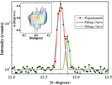 | ||
| Fig. 4 θ–2θ sum-scan (i.e. summation of 23 θ–2θ scans with a △ω spread of 0.15°) around 001 STO reflection of the TiO2/STO film. Data refer to experimental points (filled circles) and to two-peaks Gaussian theoretical fitting curves (red and green curves). In the inset the θ–2θ vs. ω map is shown. | ||
Based on the EDS data, the HAADF contrast and the diffractogram in S1, we claim that during deposition, at the growing front of TiO2, the cooperative growth of two phases, namely STO and a Sr deficient SrxTiO2+y phase (x, y < 1), is enabled due to the thermal reactivity of TiO2 with the perovskite substrate. Such a phenomenon can be attributed to the migration of Sr atoms from the STO substrate towards the film surface. Sr is thus progressively incorporated by the TiO2 growing front18,19 eventually yielding the epitaxial stabilization of a Sr-deficient region with perovskite structure. This interphase is coherent with the STO substrate and extends over a 20 nm thick region. Notably, both the Sr migration and the epitaxial stabilization of the thermodynamically unstable SrxTiO2+y phase are only observed when TiO2 is grown on atomically flat TiO2-terminated STO substrates.19 However, when TiO2 is grown on untreated STO surfaces, anatase has a relaxed structure, consistently with earlier works.9 This evidence supports the idea that SrxTiO2+y is only stabilized under biaxial strain. As revealed by XRD performed on the as-grown samples, we exclude that our observations are affected by the ion damage during TEM specimen preparation, which is known could determine a different microstructure.10
The above results underscore that in both the TiO2/LAO and TiO2/STO samples interdiffusion phenomena, not thoroughly investigated in previous works, occur between the substrate and the film region, leading to the formation of adjacent regions with different density. In the case of TiO2/LAO, Al diffuses into the growing anatase TiO2 film without affecting its crystallographic structure. The profile of diffusion extends over a 20 nm thick region away from the substrate and the resulting phase keeps a good crystallographic match with the LAO substrate. When TiO2 is grown on STO, Sr also migrates from the substrate to the film region. However, such a migration is here accompanied by a change in the structural arrangement of the growing film. The epitaxial stabilization of thermodynamically unstable phases is quite frequent in oxide epitaxy20–23 and is strictly related to the balance between volume and surface contributions to the Gibbs energy of the film islands during the nucleation. It is suggestive to relate the different crystal structures originated by the migration of Al/Sr cations to their corresponding ionic radii: the smaller size of the Al ions does not in fact generate structural modification in the TiO2 anatase structure. Nevertheless, it is remarkable that in both the systems, in spite of the completely different properties of the substrates (e.g. bonding energy, energy surfaces, cation diffusion length) the diffusion profile of Al and Sr ions extends over about the same distance. Such an issue is of fundamental interest since LAO and STO are usually considered as ideal substrates for anatase. Moreover, the issue of Al interdiffusion is also relevant in connection with the isostructural LAO/STO interfaces, where the same sequence of planes (TiO2–AlO) is present, even though in reverse order.16 Finally, the observation of a Sr-deficient epitaxial interphase at TiO2/STO interfaces has implications for fundamental knowledge as well as for technological perspectives: the TiO2/SrxTiO2+y/SrTiO3 heterostructure could be engineered to display ad hoc functionalities.
Conclusions
In summary, we investigated the nanostructural arrangement of anatase TiO2 thin films on LAO and STO substrates. HRTEM, HAADF and EDS analyses unveiled the occurrence of interdiffusion phenomena connected to a peculiar reactivity of TiO2 with perovskite substrates. Such an exhaustive investigation allowed us to shed light on the nature and fundamental properties of the interphase layers only achievable by highly advanced local probe techniques. Our findings open intriguing perspectives toward the possibility of engineering new heterostructures with targeted properties. Our work therefore provides fundamental insights for the optimization of the heteroepitaxial growth of TiO2 and for the advancement in the knowledge of LAO and STO as substrates as well as for the general issue of intrinsic oxide-interface roughening and engineering.Acknowledgements
E. Cociancich is gratefully acknowledged for the assistance in the TEM specimen preparation. Valuable and fruitful scientific discussions with P. Orgiani are thankfully acknowledged. R.C.'s research activity has received funding from the European Community's Seventh Framework Programme 2007–2011 under grant agreement no. 212348 NFFA.Notes and references
- J. Mannhart and D. Schlom, Science, 2010, 327, 1607 CrossRef CAS.
- S. A. Chambers, Adv. Mater., 2010, 22, 219 CrossRef CAS.
- B. Weinberger and R. Garber, Appl. Phys. Lett., 1995, 66, 2409 CrossRef CAS.
- J. P. Chen and R. T. Yang, J. Catal., 1993, 139, 277 CrossRef CAS.
- G. E. Jellison, F. A. Modine and L. A. Boatner, Opt. Lett., 1997, 22, 1808 CrossRef CAS.
- H. L. M. Chang, H. You, J. Guo and D. J. Lam, Appl. Surf. Sci., 1991, 48–49, 12 CrossRef CAS.
- M. Murakami, Y. Matsumoto, K. Nakajima, T. Makino, Y. Segawa, T. Chikyow, P. Ahmet, M. Kawasaki and H. Koinuma, Appl. Phys. Lett., 2001, 78, 2664 CrossRef CAS.
- S. Yamamoto, T. Sumita, T. Sugiharuto, A. Miyashita and H. Naramoto, Thin Solid Films, 2001, 401, 88 CrossRef CAS.
- A. Lotnyk, S. Senz and D. Hasse, Thin Solid Films, 2007, 515, 3439 CrossRef CAS.
- X. Weng, P. Fisher, M. Skowronski, P. A. Salvador and O. Maksimov, J. Cryst. Growth, 2008, 310, 545 CrossRef CAS.
- Z. Wang, W. Zeng, L. Gu, M. Saito, S. Tsukimoto and Y. Ikuhara, J. Appl. Phys., 2010, 108, 113701 CrossRef.
- J. C. H. Spence, Experimental High-Resolution Electron Microscopy, Oxford University Press, Oxford, 2nd edn, 1988, p. 87 Search PubMed.
- E. Carlino, in Beam Injection Based Nanocharacterization of Advanced Materials, ed. G. Salviati, T. Sekiguchi, S. Heun and A. Gustafsson, Research Signpost 37/661 (2) Fort P.O. Trivandrum-695 023, Kerala, India, 2008, p. 237 Search PubMed.
- L. A. Bursill and G. J. Wood, Philos. Mag. A, 1978, 38, 673 CrossRef CAS.
- R. Shirley, M. Kraft and O. R. Inderwildi, Phys. Rev. B: Condens. Matter Mater. Phys., 2010, 81, 075111 CrossRef.
- N. Nakagawa, H. Y. Hwang and D. A. Muller, Nat. Mater., 2006, 5, 204 CrossRef CAS.
- E. Carlino and V. Grillo, Phys. Rev. B: Condens. Matter Mater. Phys., 2005, 71, 235303 CrossRef.
- T. Kubo and H. Nozoye, Surf. Sci., 2003, 542, 177–191 CrossRef CAS.
- M. Radović, M. Salluzzo, Z. Ristić, R. Di Capua, N. Lampis, R. Vaglio and F. Miletto Granozio, J. Chem. Phys., 2011, 135, 034705 CrossRef.
- U. Scotti di Uccio, F. Miletto Granozio, A. Di Chiara, F. Tafuri, O. I. Lebedev, K. Verbist and G. van Tendeloo, Phys. C, 1999, 321, 162 CrossRef CAS.
- F. Ricci, M. F. Bevilacqua, F. Miletto Granozio and U. Scotti di Uccio, Phys. Rev. B: Condens. Matter, 2002, 65, 155428 CrossRef.
- U. Scotti di Uccio, F. Bevilacqua, G. G. Condorelli, G. Mascolo, F. Ricci and F. Miletto Granozio, Eur. Phys. J. B, 2004, 41, 3 CrossRef.
- F. Miletto Granozio and U. Scotti di Uccio, J. Alloys Compd., 1997, 251, 56 CrossRef.
| This journal is © The Royal Society of Chemistry 2012 |