Direct force producing uniform ultra-thin chitosan films by atomic force microscopy
Huiling
Zhao†
a,
Shuai
Zhang†
b,
Qiang
Li
b,
Yinli
Li
a,
Bo
Liu
*a,
Flemming
Besenbacher
b and
Mingdong
Dong
*b
aInstitute of Photo-biophysics, School of Physics and Electronics, Henan University, Kaifeng, 475004, Henan, P.R. China. E-mail: boliu@henu.edu.cn
bInterdisciplinary Nanoscience Center (iNANO), Department of Physics and Astronomy, University of Aarhus, DK-8000 Arhus C, Denmark. E-mail: dong@inano.au.dk; Fax: (+45) 87155892
First published on 30th January 2012
Abstract
Biopolymer chitosan plays an important role in functional nanomaterials, tissue engineering and other biological applications. Chitosan thin films have also been involved in many optical phenomena in living organisms, which potentially allows the use of chitosan for optical applications. However, it is rather difficult to produce uniform thin chitosan films because of its intrinsic viscoelasticity. Here we report the fabrication of uniform ultra-thin chitosan films with a thickness of several nanometres using a two-step physical approach with the help of spin coating and mechanical manipulation.
Polysaccharide is one of the major classes of biopolymers, and plays diverse roles in living organisms.1–3 Amino polysaccharides, the most interesting in producing biological thin films, have been studied extensively.4–6 Chitosan, one of the amino polysaccharides, a derivative (obtained by removing enough acetyl groups) of chitin, is a renewable source, being extracted from the shells of marine crustaceans, fungi and so on.7,8 Recently chitosan has received much attention from researchers working in various fields, due to its unique chemical, physicochemical, and biological properties.9–13 The biocompatibility of chitosan ensures its being used in tissue engineering as a bio-structuring material (temporary replacement of skin and bone tissue), for example in components of artificial blood vessels and valves, and in implants in cosmetic surgery.14–17 Interestingly, it has been fully proved that multiple layers of chitin are related to the diversity of the colour found in nature.18–21 This is related to its optical phenomena, such as reflection, refraction, and alternating-layer thin-film interference.22 One convincing example is vertical diffraction gratings, found in nature-employed layers, which are a few nm in depth.23 These layers can be arranged in a regular stack, in alternating layers of equal thickness, in a chirped stack with layers of decreasing thickness, or in a chaotic stack with layers of random thickness.24 For industry applications (such as optical devices, or functional surface coating) chitosan films with defined thickness and low roughness over a relatively large area are expected. Furthermore, optically transparent properties (non-absorbing and non-scattering) of chitosan films require nanoscale thickness. Recently spin coating has been the method commonly used for the fabrication of polymer-like films. By varying spin speeds, chitosan films, thicknesses in the range of 120–200 nm with a standard deviation of 6–10 nm,22 can be formed reproducibly. However, forming uniform ultra-thin chitosan films below 10 nm seems to remain out of the ability of this method.
In this communication, we report a two-step strategy (Fig. 1) to produce uniform ultra-thin chitosan films with small height variation, by means of the two physical approaches of spin coating and atomic force microscopy (AFM) mechanical manipulation. AFM is a powerful surface technique, allowing the manipulation of nanomaterials with defined forces.25–27 Moreover the uniformity could be monitored and evaluated easily. Hence, it provides the possibility to fabricate ultra-thin chitosan films, which is out of the capability of the spin coating method itself. Such ultra-thin films may have potential applications in constructing vertical gratings with certain reflective and transparent properties. At the same time, the two-step method allows the preparation of ultra-thin films from high intrinsic viscoelasticity polymers for surface functionalization.
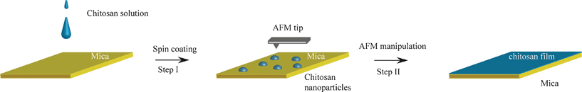 | ||
| Fig. 1 Schematic of the creation of a uniform ultra-thin chitosan film. Step I: deposition of soluble chitosan solution onto the mica substrate and spin coating to obtain chitosan nanoparticles; Step II: manipulation of the nanoparticle layer by means of an AFM tip with constant exerted force to fabricate the ultra-thin chitosan film. | ||
For thin film fabrication, the physical properties of selected substrates have a great influence on the thickness of the film. In this work hydrophilic mica (contact angle ∼20°)28 was used as the supporting plate for the chitosan film composed of nanoparticles. Due to the highly hydrophilic properties, the mica surface could adsorb a water layer to spread the chitosan molecules. In addition, the negatively charged mica further allowed the spread of positive chitosan solution/nanoparticles across the surface. Last but not least, the atomic flat mica surface provided an ideal template to make uniform low height-variation ultra-thin films.
During the experimental process, we used a fully soluble solution of chitosan with short chains (the chemical structure is given in Fig. 2a). The chain length of the chitosan polymer was shortened by using acid cleavage to increase its solubility to stabilize the chitosan nanoparticles against fluctuations of temperature and humidity. Initially, 100 μl chitosan solution was deposited onto the substrate. By spin coating at 500 rpm at room temperature, the initial coating could be formed (shown as step I in Fig. 1). However, due to the highly viscoelastic properties of chitosan, such little chitosan solution could not form a continuous film by spin coating itself. Though, increasing the volume of chitosan solution would result in the formation of a coherent film, only a thick film could be formed. It is very difficult to fabricate thin films only through the spin-coating method. On the other hand, discontinuous chitosan nanoparticles were formed from the spin coating of a solution with a small volume. Additional physical manipulation is required to produce a continuous thin film. Before the AFM manipulation process, the morphology of the chitosan nanoparticles was further characterized, as the height of the nanoparticles would influence the final thickness of the chitosan film strongly, which can lead to different optical properties. And a broad height distribution of the nanoparticles makes it difficult for the AFM probes to apply a constant force to the neighbouring chitosan nanoparticles, therefore nanoparticles with uniform particle size are required.
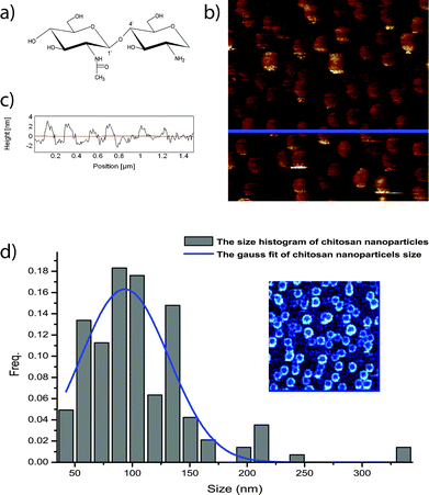 | ||
| Fig. 2 (a) Chemical structure of carbohydrate chitosan; (b) morphology image of chitosan nanoparticles; (c) line profile of the blue solid line in (b), and the height of chitosan nanoparticles is around 2.5 nm; the size of the image is 1.5 μm by 1.5 μm; (d) size distribution of the chitosan nanoparticles, and the height is 93.3 ± 36.8 nm. (inset phase image of the chitosan nanoparticles). | ||
AFM with tapping mode was used to characterize the chitosan nanoparticle layer under ambient conditions. Fig. 2b shows an AFM morphology image of the chitosan nanoparticles on the mica surface after spin coating. The line profile, Fig. 2c, indicating the blue solid line in Fig. 2b, shows the typical height of the particles is around ∼2.5 nm. The height variations of the nanoparticles are very small, which means that the force between the nanoparticles and the AFM probe can be kept constant easily. On the other hand, by fitting a Gaussian distribution to the size histogram of the chitosan particles (Fig. 2d), the diameter of the nanoparticles is found to be 93.3 ± 36.8 nm. The small diameter variation results from the viscoelasticity of chitosan, which restricts the movement of chitosan, and exerts a negative effect on chitosan distribution.
After the characterization of the chitosan nanoparticles on mica, chitosan particles were further executed by Step II (Fig. 1). AFM, as a key type of surface probe microscopy, is used to detect force changes across surfaces, which allows us to monitor the morphology change. Hence, it is possible to accurately control the force exerted on a certain position through adjusting the parameters, such as the set point and drive amplitude. During the manipulation, 5∼10 nN force was applied to the chitosan particles forming ultra-thin films with the help of AFM. Besides controlling the force precisely, another two important factors, humidity and temperature, also needed to be considered carefully, as the viscoelastic properties of the chitosan particles can be influenced strongly by these two factors. If the ambient humidity or temperature alters suddenly, the viscoelastic properties of chitosan will change dramatically. As a result, the chitosan film may swell and crack during the scanning process. The humidity (∼60%) and room temperature were kept constant in the whole process. Another reason why high humidity was used is that in ambient air surroundings, a water layer is captured by the chitosan nanoparticles and mica substrate. Wettability determines solid surface properties.29–31 Hence, the narrow gap capillary phenomenon between the AFM tip and the sample will appear.32–35 When the tip approaches the sample surface, it is proposed that the chitosan molecules could be transported from the substrate to the tip and vice versa, depending on the water humidity and the substrate wetting properties, which results in the spread of the ultra-thin chitosan film.
Another advantage of AFM is that it allows one to monitor the whole manipulation process in situ. By capturing the images continuously, a series of time-lapse AFM topographies were recorded during the manipulation of one certain region of the chitosan nanoparticle layer sample. The resolution is 512 pixels by 512 pixels per image with 1 Hz scan frequency. The velocity of the probe is 1.5 μm s−1. So the time span between the two adjacent images is about 8.5 min. The close-up images (from T1 to T20 in Fig. 3a) were recorded over three hours. In Fig. 3a, it is obvious that the particles disappear and merge into a large film gradually, and surface coverage increases at the same time. Then the initial image of nanoparticles (T1) and the final film (T20) were further analyzed through the height distribution of chitosan, respectively (Fig. 3b and Fig. 3c). The height of the background was referred to the relative zero value. At the T1 time stage, the height of these nanoparticles is 2.2 ± 1.1 nm with low coverage and the background is dominant (Fig. 3b). However, at the end of the series of images (T20), the peak of the background has nearly disappeared, while the peak of the chitosan film has grown dramatically (Fig. 3c). Image T20 further proves that the film grows across the mica surface and dominates the whole surface. The thickness of the chitosan film is 2.9 ± 0.8 nm (Fig. 3c). Compared with previous work,22 the height variation of the fabricated ultra-thin film is much smaller; it could be concluded that the ultra-thin chitosan film should be homogeneous. All in all, by analyzing Fig. 3 systematically, a uniform ultra-thin chitosan film with height ∼3 nm was created successfully.
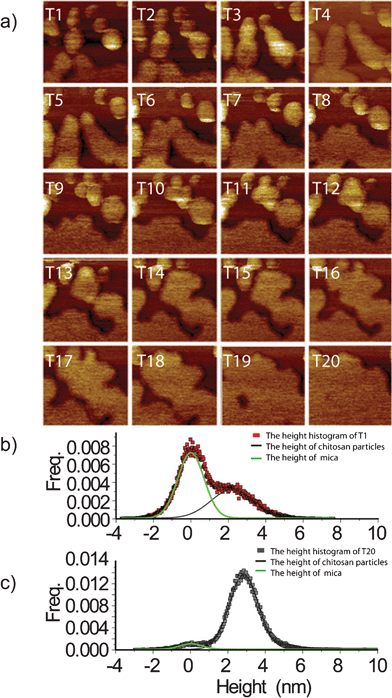 | ||
| Fig. 3 (a) Time-lapse in situ morphology images of chitosan nanoparticles/film; (b) height histogram of T1; (c) height histogram of T20; the size of the images is 500 nm by 500 nm. | ||
In this communication, we have reported a two-step physical method to prepare uniform ultra-thin (2.9 ± 0.8 nm) chitosan films by means of the combination of spin coating and AFM-based manipulation. This method has some advantages that the classic methods do not have. First, it can be operated under mild conditions, friendly to biomolecules, which is hard for traditional chemical vapor deposition (CVD)36 and molecular beam epitaxy (MBE)37 approaches. Second, it decreases the film thickness to several nanometres, which is out of the capability of the single spin coating method.
By keeping the AFM probe tip scanning with a controlled stable force, under certain humidity and temperature with the capillary effect, the chitosan nanoparticles can be transformed into ultra-thin films with a small height distribution of about three nanometres. This novel strategy opens a new way for the construction of a chitosan vertical diffraction grating with certain reflective properties. Such chitosan films can potentially be used to improve the optical quality of films, for example modifying the refractive index. The concept can be applied not only on mica surfaces, but also on other solid substrates, which can be further applied to nanoscale surface functionalization. In the end, though this work is mainly a fundamental one, multiple cantilever arrays,38,39 thousands of parallel AFM probes, may be a good choice to facilitate it, in future, to fabricate large size ultra-thin films for industrial applications.
References
- S. Geresh and S. A. Malis, Bioresour. Technol., 1991, 38, 195–201 CrossRef CAS.
- L. Diez, Z. Guadalupe, B. Ayestaran and F. Ruiz-Larrea, J. Agric. Food Chem., 2010, 58, 7731–7739 CrossRef CAS.
- M. Y. K. Leung, C. Liu, J. C. M. Koon and K. P. Fung, Immunol. Lett., 2006, 105, 101–114 CrossRef CAS.
- C. F. Hu, J. H. Li, D. Y. Yang, Y. J. Pan and H. T. Wan, J. Nat. Prod., 2010, 73, 1489–1493 CrossRef CAS.
- F. Di Renzo, R. Valentin, M. Boissiere, A. Tourrette, G. Sparapano, K. Molvinger, J. M. Devoisselle, C. Gerardin and F. Quignard, Chem. Mater., 2005, 17, 4693–4699 CrossRef CAS.
- O. G. Jones, J. Adamcik, S. Handschin, S. Bolisetty and R. Mezzenga, Langmuir, 2010, 26, 17449–17458 CrossRef CAS.
- J. M. Dorioz, M. Robert and C. Chenu, Geoderma, 1993, 56, 179–194 CrossRef.
- U. Edlund, Y. Z. Ryberg and A. C. Albertsson, Biomacromolecules, 2010, 11, 2532–2538 CrossRef CAS.
- M. Y. Cheng, J. U. Deng, F. Yang, Y. D. Gong, N. M. Zhao and X. F. Zhang, Biomaterials, 2003, 24, 2871–2880 CrossRef CAS.
- M. Hiorth, I. Tho and S. A. Sande, Eur. J. Pharm. Biopharm., 2003, 56, 175–182 CrossRef CAS.
- A. P. Martinez-Camacho, M. O. Cortez-Rocha, J. M. Ezquerra-Brauer, A. Z. Graciano-Verdugo, F. Rodriguez-Felix, M. M. Castillo-Ortega, M. S. Yepiz-Gomez and M. Plascencia-Jatomea, Carbohydr. Polym., 2010, 82, 305–315 CrossRef CAS.
- M. Vargas, A. Albors, A. Chiralt and C. Gonzalez-Martinez, Food Hydrocolloids, 2009, 23, 536–547 CrossRef CAS.
- Q. Wang, Z. F. Dong, Y. M. Du and J. F. Kennedy, Carbohydr. Polym., 2007, 69, 336–343 CrossRef CAS.
- J. L. Doublier, C. Garnier, D. Renard and C. Sanchez, Curr. Opin. Colloid Interface Sci., 2000, 5, 202–214 CrossRef CAS.
- C. O. Ferreira, C. A. Nunes, I. Delgadillo and J. A. Lopes-da-Silva, Food Res. Int., 2009, 42, 807–813 CrossRef CAS.
- S. Puttipipatkhachorn, J. Nunthanid, K. Yamamoto and G. E. Peck, J. Controlled Release, 2001, 75, 143–153 CrossRef CAS.
- S. Rivero, M. A. García and A. Pinotti, Carbohydr. Polym., 2010, 82, 270–276 CrossRef CAS.
- H. Ghiradella, Appl. Opt., 1991, 30, 3492–3500 CrossRef CAS.
- E. A. Monroe and S. E. Monroe, Science, 1968, 159, 97–98 Search PubMed.
- A. R. Parker, Mater. Today, 2002, 5, 26–31 CrossRef CAS.
- M. Srinivasarao, Chem. Rev., 1999, 99, 1935–1961 CrossRef CAS.
- F. S. Ligler, B. M. Lingerfelt, R. P. Price and P. E. Schoen, Langmuir, 2001, 17, 5082–5084 CrossRef CAS.
- A. R. Parker, Am. Sci., 1999, 87, 248–255 Search PubMed.
- A. R. Parker, J. Exp. Biol., 1998, 201, 2343–2347 CAS.
- M. Dong and O. Sahin, Nat. Commun., 2011, 2, 247 CrossRef.
- M. D. Dong, S. Husale and O. Sahin, Nat. Nanotechnol., 2009, 4, 514–517 CrossRef CAS.
- O. Sahin, S. Magonov, C. Su, C. F. Quate and O. Solgaard, Nat. Nanotechnol., 2007, 2, 507–514 CrossRef.
- A. Keller, M. Fritzsche, Y.-P. Yu, Q. Liu, Y.-M. Li, M. Dong and F. Besenbacher, ACS Nano, 2011, 5, 2770–2778 CrossRef CAS.
- M. Chen and F. Besenbacher, ACS Nano, 2011, 5, 1549–1555 CrossRef CAS.
- K. Koch, B. Bhushan and W. Barthlott, Soft Matter, 2008, 4, 1943–1963 RSC.
- P. G. de Gennes, Rev. Mod. Phys., 1985, 57, 827–863 CrossRef CAS.
- M. Binggeli and C. M. Mate, Appl. Phys. Lett., 1994, 65, 415–417 CrossRef CAS.
- M. Fujihira, D. Aoki, Y. Okabe, H. Takano, H. Hokari, J. Frommer, Y. Nagatani and F. Sakai, Chem. Lett., 1996, 499–500 CrossRef CAS.
- L. Xu, A. Lio, J. Hu, D. F. Ogletree and M. Salmeron, J. Phys. Chem. B, 1998, 102, 540–548 CrossRef CAS.
- R. D. Piner, J. Zhu, F. Xu, S. H. Hong and C. A. Mirkin, Science, 1999, 283, 661–663 CrossRef CAS.
- A. Henry, J. ul Hassan, J. P. Bergman, C. Hallin and E. Janzen, Chem. Vap. Deposition, 2006, 12, 475–482 CrossRef CAS.
- W. P. McCray, Nat. Nanotechnol., 2007, 2, 259–261 CrossRef CAS.
- P. Vettiger, M. Despont, U. Drechsler, U. Durig, W. Haberle, M. I. Lutwyche, H. E. Rothuizen, R. Stutz, R. Widmer and G. K. Binnig, IBM J. Res. Dev., 2000, 44, 323–340 CrossRef CAS.
- M. Favre, J. Polesel-Maris, T. Overstolz, P. Niedermann, S. Dasen, G. Gruener, R. Ischer, P. Vettiger, M. Liley, H. Heinzelmann and A. Meister, J. Mol. Recognit., 2011, 24, 446–452 CrossRef CAS.
Footnote |
| † These authors contributed equally to this work. |
| This journal is © The Royal Society of Chemistry 2012 |