Large surface photovoltages observed at methyl-terminated silicon surfaces synthesised through a two-step chlorination-alkylation method†
Nicholas
Alderman
*ab,
Lefteris
Danos
a,
Martin C.
Grossel
b and
Tom
Markvart
a
aSolar Energy Laboratory, Engineering Sciences, Faculty of Engineering and the Environment, University of Southampton, Highfield, Southampton, UK SO17 1BJ. E-mail: N.Alderman@soton.ac.uk; Tel: +44 2380 596769
bFaculty of Natural and Environmental Science, University of Southampton, Highfield, Southampton, UK SO17 1BJ
First published on 10th July 2012
Abstract
Methylation of the silicon surface through a chlorination-alkylation method has been used to improve the electronic properties of silicon. Upon alkylation of the surface, an increase in the minority carrier recombination lifetime and the surface photovoltage is observed, in line with an increase in surface charge. A likely explanation of this unusually large band bending is charge accumulation during the removal of chlorine from the surface.
Covalently bonded organic monolayers on silicon surfaces have been shown to give excellent passivation properties1,2 and oxide resistance3 using minority recombination lifetime and ellipsometry measurements. Nevertheless, the surface photovoltage (SPV) of alkylated silicon surfaces has not been widely investigated and can provide an important insight into the electrostatic properties of the surface. We present a new insight into the mechanism of passivation from the attached methyl layer involving trapped charges on the silicon surface.
Surface properties of semiconductors are becoming increasingly important due to the reduced size of micro-electronics and the search for ever more efficient devices such as solar cells.4 Alkylation of silicon surfaces can lead to excellent passivation properties as well as being a lower-temperature technique than current passivation methods.5 This gives the advantage of having a lower impact on bulk silicon properties.
Organic modification of semiconductor surfaces would therefore be an attractive solution to reduce electron-hole recombination in these devices as well as providing a test-bed for further functionalisation. Recently a large amount of research has examined the possibility of secondary functionalisation of alkylated silicon surfaces.6,7 It is therefore of importance that we understand the electronic properties and the mechanism of functionalization of these surfaces in detail.
Covalently bound monolayers attached on silicon were first produced by Lindford and Chidsey in 1993.8 These were synthesised by immersing a hydrogen-terminated silicon surface in diacyl peroxides and heating, resulting in pyrolysis which produced alkyl radicals.
In 1996, Lewis et al. proposed a route for alkylation of silicon surfaces using a two-step halogenation/Grignard route.9 Since then, several other techniques for attaching organic monolayers on to silicon have been investigated, involving ultra-violet light,10 transition metal complexes,2 electrochemical grafting11 or thermal grafting.12,13
The technique used in this paper has been modified from the method of Lewis et al. as this has been shown to have greater versatility for the introduction of small alkyl chains whilst retaining excellent chemical and electrical properties.14 This method has also been found to produce monolayers for a wide range of silicon substrates; Si(100),3 Si(111),1 silicon nanowires15 and porous silicon,16 allowing greater flexibility in the choice of the substrate.
Recent studies into surface photovoltage measurements on organically passivated silicon surfaces have been focused on those produced by either thermal reactions with alkenes and alcohols or those produced electrochemically. Literature examples have shown an improvement in surface photovoltage, giving values of 40–80 mV.17,18 Synchrotron photoelectron spectroscopy suggests that samples produced by the two-step chlorination-alkylation technique are close to being in a flat-band state.19
These varied surface photovoltage results suggest that there might be a different mechanism of passivation of the organic monolayers depending on the preparation method. It is therefore important to gain more detailed insight into the factors which control the electronic properties of the passivation layers.
The mechanism of the chlorination-alkylation reaction involves the generation of charged species and the flow of electrons within the silicon sample.1 Therefore charging of the alkylated surface could occur during step 1 of the alkylation reaction as shown in Scheme 1.
 | ||
| Scheme 1 Mechanism of the alkylation step of the synthesis. | ||
 | ||
| Scheme 2 Synthesis of alkyl monolayers on silicon. | ||
Charging of semiconductor surfaces has been of great interest recently, with investigations focusing on charging by immersion in chemicals,20 corona discharge21 and atomic layer deposition.22 This work provides a further insight into the effect of charging on semiconductor surfaces arising from changes in surface bonding.
Materials and methods
All chemicals were obtained anhydrous from Sigma-Aldrich, stored under nitrogen and used as supplied. Freshly prepared Grignard solutions were used to maximise the surface coverage obtained.23The silicon samples (Siltronix, 10 mm × 10 mm, n-type, double side polished with a resistivity of 25.5 Ω cm−1 and guaranteed bulk lifetime of >1000 μs) were cleaned in a solution of hydrogen peroxide and sulphuric acid (1![[thin space (1/6-em)]](https://www.rsc.org/images/entities/char_2009.gif) :
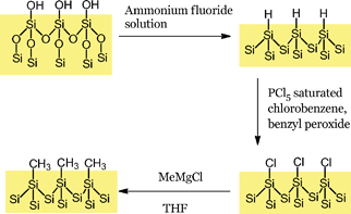
:![[thin space (1/6-em)]](https://www.rsc.org/images/entities/char_2009.gif) 3) for 30 min prior to use. After a thorough rinse in ultra-pure water (>18 MΩ cm−1) the samples were etched in degassed ammonium fluoride for 15 min. The freshly etched sample was then transferred into a glovebox for surface functionalisation (see Scheme 2).
3) for 30 min prior to use. After a thorough rinse in ultra-pure water (>18 MΩ cm−1) the samples were etched in degassed ammonium fluoride for 15 min. The freshly etched sample was then transferred into a glovebox for surface functionalisation (see Scheme 2).
The hydrogen-terminated surface was immersed in a saturated solution of phosphorus pentachloride in chlorobenzene, to which a few grains of benzyl peroxide had been added, for 2 h at 110 °C.
After washing the sample in chlorobenzene and tetrahydrofuran, the chlorinated sample was placed in a 1 M solution of methylmagnesium chloride in THF and heated for 24 h at 110 °C. After sonicating in a 1![[thin space (1/6-em)]](https://www.rsc.org/images/entities/char_2009.gif) :
:![[thin space (1/6-em)]](https://www.rsc.org/images/entities/char_2009.gif) 10 solution of acetic acid–methanol and drying under nitrogen, spectroscopic measurements were carried out.
10 solution of acetic acid–methanol and drying under nitrogen, spectroscopic measurements were carried out.
It was found that samples with the highest minority recombination lifetimes were synthesised when the reaction mixtures were heated to 110 °C and freshly-opened bottles of the Grignard were used. It was observed that storage of the Grignard reagent in the glovebox led to a reduced lifetime and infrared data suggested a lower surface coverage with reduced passivating effects. Similar observations have been reported in the literature.23
All infrared spectra were obtained using a Bruker Tensor 27 spectrometer fitted with a mercury-cadmium-telluride (MCT) detector and a PIKE VEEMAX II variable angle reflection accessory which was set to 37° from normal with S-polarisation of the reflected beam. A total of 500 scans were obtained between 600 and 4000 cm−1 with background scans of a native oxide sample subtracted from each spectrum.
X-ray photoelectron spectroscopy (XPS) was performed on samples using a Thermo-Scientific ME17 Thetaprobe XPS spectrometer with a 400 μm spot size.
The effective recombination lifetimes of the samples were measured on a Sinton Instruments WCT-120 wafer-lifetime tool. This inductively measures the photoconductance over time of a decaying light pulse. The original fitting parameters were modified to take into account the reduced area of our samples. As the lifetime measured here is an effective lifetime, it will contain a contribution from both the bulk and surface recombination. As the bulk lifetime of the samples were high (guaranteed >1000 μs), the bulk contribution will be negligible.
SPV measurements were performed on a scanning Kelvin Probe system (SKP5050) from KP Technology. The Kelvin probe measures the work function of the surface, and by taking measurements in dark and illuminated conditions both the bent and flat-band conditions can be measured. The difference between the two measurements is known as the surface photovoltage (SPV) and is directly related to the amount of band bending at the surface.
The samples were illuminated by optical fibre whilst in the Kelvin Probe with a xenon lamp as the source. The illumination intensity was varied until the surface photovoltage reached saturation.
Results and discussion
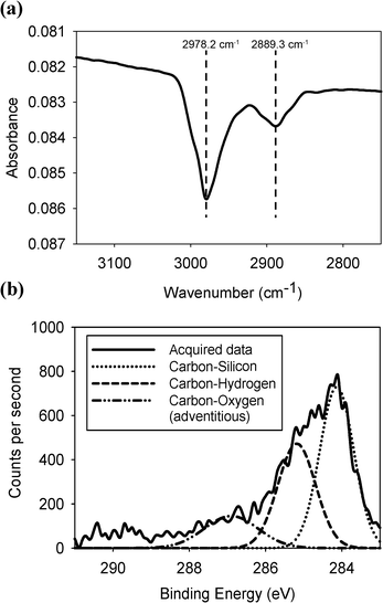
A section of the IR spectrum showing the methyl group C–H stretches obtained from a methylated silicon surface is shown in Fig. 1. The methyl-terminated surface contains two peaks at 2978.2 and 2889.3 cm−1, corresponding to a symmetric and an asymmetric C–H stretch of a CH3 unit in agreement with previous studies.24 We found that the best spectra were produced when the reflected beam was s-polarised. | ||
| Fig. 1 (a) Infrared spectrum of the C–H stretching region and (b) the XPS data of the carbon 1s peak of the methyl terminated surface. | ||
X-ray photoelectron spectroscopy confirmed that the methyl group was covalently bonded to the silicon surface, as shown in Fig. 1. Peaks for carbon bonded to carbon and silicon (with some adventitious carbon bonded to oxygen) were observed. In the silicon 2p binding energy region, no silicon-oxygen peaks were visible confirming that no surface oxidation had occurred. This also demonstrated that the carbon-oxygen peak observed in the carbon 1s binding region was caused by either physisorbed methanol from the washing step or by carbon dioxide (see ESI†).
Kelvin probe (SPV) measurements were recorded at each stage of the processing. Table 1 shows the results obtained from SPV and recombination lifetime measurements on each stage of the methyl attachment on silicon surfaces. An improvement in the SPV signal was observed when moving from the native oxide samples to the hydrogen-terminated surface. However the effective recombination lifetimes remained low.
Moving from the hydrogenated to the chlorinated surface, the SPV signal was diminished indicating a flat band. This is likely to be due to the higher electronegativity of the chlorine when compared to that of silicon, allowing charge neutralisation of the surface and reducing band bending. Once again, the effective lifetime remained low, indicating that the surface photovoltage measured is not directly correlated to the lifetime measured—therefore, in these samples we have both flat bands due to the electronegativity of chlorine removing surface charge, and the presence of surface states allowing recombination to occur.
Upon alkylation of the surface with a Grignard reagent a substantial increase in SPV to around 450 mV was observed. This is indicative of larger band bending than even that present in the native oxide sample, showing a surface which is highly charged. Interestingly, the effective recombination lifetime increases from under 10 μs to over 100 μs.
A high SPV and lifetime was observed on multiple samples, and contradicts a large amount of research on organic layers produced by alternative methods.17 It was widely believed that samples with a high lifetime would be in an almost flat-band state when organically passivated—the surface states that promote recombination would not be present after passivation and therefore there would be no surface charge. However this is not observed on samples produced by the chlorination-alkylation technique.
The SPV remained high on these samples even after multiple washes in methanol–acetic acid, confirming that the band bending observed was not due to adsorbed magnesium salts or any other ions present on the surface.
To confirm that the observed increase in SPV was not due to the presence of magnesium in the surface depletion layer, a chlorinated surface was heated to the reaction temperature in a solution of magnesium chloride in tetrahydrofuran. Kelvin probe measurements on these samples still showed a low SPV of around 10 mV. Therefore evidence suggests that the increase in SPV is not due to the inclusion of charged magnesium salts on the surface.
The observed large SPV signal is likely to be due to the charging of the silicon surface during step 1 of the reaction scheme. During this step, the negative charge could be trapped in slow traps, which would give a high SPV for extended periods of time. This step would allow the surface to become more charged than native oxide samples, increasing the band bending observed and therefore the SPV obtained. Repeating the measurements on samples that were stored in air for two weeks still showed a very high SPV (within 5% of SPV values from freshly made samples). This is a key difference in the reaction of chlorinated surfaces with Grignard reagents, and could explain why the increase in SPV is not observed with other organic monolayer synthesis methods.17,25
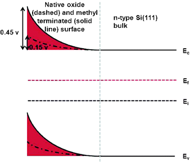
A high SPV is consistent with a highly negatively charged silicon surface, which could arise during step 1 in the reaction shown in Scheme 1. This has the effect of bending the surface bands, as shown in Fig. 2.
 | ||
| Fig. 2 The surface bands as measured by Kelvin probe for both the native oxide and methyl terminated surface. | ||
Interestingly, samples produced by the two-step chlorination-alkylation technique show excellent passivation properties when compared to other organic monolayers produced on silicon. A likely explanation for this observation is that the band bending reduces the concentration of the majority carriers (electrons) at the surface, and increases the gap between the Fermi level and the conduction band (Fig. 2).
The passivation observed on the samples is different from the conventional picture; that well passivated samples are in a flat band state due to the removal of surface states. However, in the samples produced by the two-step chlorination-alkylation method, both charging of the surface and removal of the surface states can combine to produce a sample with high effective recombination lifetimes.
A likely explanation is that surface states are removed by the formation of silicon-carbon bonds, as well as fixed charge trapping which does not change with the Fermi level. This results in band bending which repels majority carriers, increasing the recombination lifetime.
Conclusions
Methyl-terminated silicon surfaces can be routinely and reproducibly synthesised through a two-step chlorination-alkylation Grignard method. This leads to the attachment of an alkyl monolayer on the surface possessing a high minority recombination lifetime and great stability in ambient conditions. This can also provide a testing ground for further surface functionalisation.Samples were characterised using X-ray photoelectron spectroscopy and infrared spectroscopy. These measurements confirmed the successful methylation of the surface, with C–H stretching bands visible in the infrared spectrum and carbon-silicon binding energies visible in the XPS spectra.
Surface photovoltage measurements of the methyl-terminated surface show a substantial value along with an increase in the effective recombination lifetime. This can be attributed to an increase in surface band bending, lowering the surface electron concentration and reducing recombination. The unusually large band bending observed is attributed to the accumulation of trapped charges during the alkylation procedure.
Acknowledgements
This work was supported by the Engineering and Physical Sciences Research Council under the Supergen program ‘Photovoltaics materials for the 21st century’ (PV21).References
- E. Nemanick, P. Hurley, B. Brunschwig and N. Lewis, J. Phys. Chem. B, 2006, 110, 14800 CrossRef CAS.
- L. Webb and N. Lewis, J. Phys. Chem. B, 2003, 107, 5404 CrossRef CAS.
- E. Nemanick, P. Hurley, L. Webb, D. Knapp, D. Michalak, B. Brunschwig and N. Lewis, J. Phys. Chem. B, 2006, 110, 14770 CrossRef CAS.
- J. Zhao, A. Wang and M. Green, Progr. Photovolt.: Res. Appl., 1999, 7, 471 CrossRef CAS.
- A. El amrani, I. Menous, L. Mahiou, R. Tadjine, A. Touati and A. Lefgoum, Renewable Energy, 2008, 33, 2289 CrossRef CAS.
- S. Puniredd, O. Assad and H. Haick, J. Am. Chem. Soc., 2008, 130, 13727 CrossRef CAS.
- P. Wagner, S. Nock and J. Spudich, J. Struct. Biol., 1997, 119, 189 CrossRef CAS.
- M. Linford and C. Chidsey, J. Am. Chem. Soc., 1993, 115, 12631 CrossRef CAS.
- A. Bansal, X. Li, I. Lauermann and N. Lewis, J. Am. Chem. Soc., 1996, 118, 7225 CrossRef CAS.
- T. Mischki, R. Donkers, B. Eves, G. Lopinski and D. Wayers, Langmuir, 2006, 22, 8359 CrossRef CAS.
- S. Vegunta, J. Ngunjiri and J. Flake, Langmuir, 2009, 118, 7225 Search PubMed.
- T. Mischki, G. Lopinski and D. Wayner, Langmuir, 2009, 25, 5626 CrossRef CAS.
- M. Sung, G. Kluth, O. Yauw and R. Maboudian, Langmuir, 1997, 13, 6164 CrossRef CAS.
- W. Royea, A. Juang and N. Lewis, Appl. Phys. Lett., 2000, 77, 1988 CrossRef CAS.
- M. Bashouti, T. Stelzner, S. Christiansen and H. Haick, J. Phys. Chem. C, 2009, 113, 14823 CAS.
- N. Kim and P. Laibinis, J. Am. Chem. Soc., 1998, 120, 4516 CrossRef CAS.
- X. Bin, T. Mischki, C. Fan, G. Lopinski and D. Wayner, J. Phys. Chem. C, 2007, 111, 13547 CAS.
- Y. Cohen, A. Vilan, I. Ron and D. Cahen, J. Phys. Chem. C, 2009, 113, 6174 CAS.
- R. Hunger, R. Fritsche, B. Jaeckel and W. Jaegermann, Phys. Rev. B: Condens. Matter Mater. Phys., 2005, 72, 45317 CrossRef.
- A. Stephens and M. Green, Sol. Energy Mater. Sol. Cells, 1997, 45, 255 CrossRef CAS.
- J. Mizsei, Appl. Surf. Sci., 2006, 252, 7691 CrossRef CAS.
- K. Weber and H. Jin, Appl. Phys. Lett., 2009, 94, 63509 CrossRef.
- S. Amy, D. Michalak, Y. Chabal, L. Wielunski, P. Hurley and N. Lewis, J. Phys. Chem. C, 2007, 111, 13053 CAS.
- L. Webb, S. Rivillon, D. Michalak, Y. Chabal and N. Lewis, J. Phys. Chem. B, 2006, 110, 7349 CrossRef CAS.
- A. Sieval, C. Huisman, A. Schonecker, F. Schuurmans, A. van der Heide, A. Goossens, W. Sinke, H. Zuilhof and E. Sudholter, J. Phys. Chem. B, 2003, 107, 6846 CrossRef CAS.
Footnote |
| † Electronic Supplementary Information (ESI) available. See DOI: 10.1039/c2ra20465g/ |
| This journal is © The Royal Society of Chemistry 2012 |
