DOI:
10.1039/C2RA21224B
(Paper)
RSC Adv., 2012,
2, 11544-11551
Rapid and large-scale synthesis of Cu nanowires via a continuous flow solvothermal process and its application in dye-sensitized solar cells (DSSCs)†
Received
19th June 2012
, Accepted 27th September 2012
First published on 1st October 2012
Abstract
Single crystalline copper nanowires with pentagonal cross sections and large aspect ratios have been successfully prepared in high yield via a continuous flow solvothermal reduction process at a low temperature. The highly crystalline filaments exhibit the face-centered cubic structure, growing mainly along the [110] direction. Both PVP and the solvent environment play an important role for the growth of nanowires. The growth mechanism has been properly discussed. We also report the flexible transparent Cu nanowire membrane electrode fabricated by coating a polymer layer as a potential replacement for the conventional FTO electrode in dye-sensitized solar cells (DSSCs). Fabricated CuNW membranes exhibit high optical transmittance and electrical conductance, which can be controlled via the synthesis process, conveniently. The efficiency of a DSSC with CuNWs increases upto 5%. The DSSC performs as well as with a FTO electrode, which indicates that the super-high aspect ratio of the Cu nanowires offers a range of electrical transport routes to connect dye loaded photo-anodes, and such an electrode has the potential to replace conventional FTO electrodes for low-cost DSSCs applications.
1 Introduction
Copper is normally the most frequently used metallic material for industrial and commercial applications, either in a finely grained poly- or single-crystalline form. In recent years, there has been growing interest in the pursuit of one-dimensional (1D) copper nanostructures, especially copper nanowires (CuNWs) with high aspect ratios, not only for their unique properties, but also for a variety of potential applications in the fields of nanoelectronics,1–3 chemical sensors,4 and biotechnology.5 In particular, CuNWs are being explored as inexpensive, electrically conducting additives to composites and transparent conducting electrodes for solar cell.6–9 These potentials are not only due to low cost, easy fabrication and compatibility with flexible substrate over large areas of CuNWs, but also because the structure of the nanowires provides a more efficient way to absorb light and extract electrons freed by light. So far, most conventional dye solar cells have been built on slabs of transparent conductive oxide (TCO) semiconductor materials such as fluorine doped tin oxide (FTO) instead of indium tin oxide (ITO), mainly because of its lower cost and higher temperature stability. However, there are several problems preventing its use for future high performance device applications. First, the greater thickness of FTO films means better light absorption, but it also means that it is more difficult for electrons to escape; second, the high temperature processing of FTO to achieve high transmittance and conductivity is not compatible with a flexible plastic substrate; third, the brittle nature means that it not suitable for flexible applications; and fourth, its rough surface causes high leakage current in solar cell devices, leading to low efficiencies. Therefore, a new transparent and conductive electrode made from NWs having the potential to overcome these defects is highly desirable. Cu is well suited for practical solar cell applications due to its much lower cost and similar work function to FTO (ca. 4.7–4.9 eV). Each CuNW is 10 to 200 nm wide and up to tens of microns long. Their length maximizes absorption, but their nanoscale diameter permits a much freer movement and collection of electrons. Additionally, cost becomes less of an issue with NWs because so little cheap raw materials are needed. The copper nanofiber networks also show much better flexibility and stretchabilty than traditional transparent films according to earlier studies.6,7,9 Thus much effort has been devoted to produce CuNWs both in experiments and in theory. The most popular techniques used to fabricate uniform artificial structures with feature sizes in the sub-200 nm range are metal organic chemical vapor deposition (MOCVD) approaches,10,11 hydrothermal methods,12–16 carbon nanotube capillary growth17–20 and electrochemical deposition lithography21etc. Even though these drastic physical and wet-chemical strategies have been developed for preparing CuNWs successfully, they always need a tedious procedure to remove the auxiliary template (SBA-15, porous aluminum oxide etc), or require complex apparatus and rigorous processing conditions. As a result, these defects made it difficult to further test theories of quantum confinement and yield samples with desirable optical, luminescent, and other important physical and chemical characteristics from the point of view of application.
In an effort to improve the applicability of nanodevices made from CuNWs, here we develop a new synthetic method that produces single-crystalline, well-faceted, thinner and longer CuNWs with pentagonal cross sections based on preliminary work.22 This synthesis was performed using a continuous flow solvethermal reduction process under mild conditions. We also proposed a front contact structure of 1D CuNWs as a potential replacement for the conventional FTO electrode applied in dye-sensitized solar cells (DSSCs), which shows low sheet resistance measured with a four-point probe and high optical transmittance comparable to the FTO electrode in the visible range that enable an excellent cell performance with regard to photovoltaic efficiency.
2 Experimental
2.1 Synthesis of CuNWs on glass substrate
All of the chemical reagents used were of analytical grade. Prior to the experiment, all glass substrates used in preparation process were cleaned successively using detergent, deionized water, acetone, and boiling isopropyl alcohol, each under ultrasonication and then treated with nitrogen purging for 15 min. To prepare feed precursor solutions for a typical synthesizing CuNWs, 0.5 mM CuCl2·2H2O (in ethanol solvent), and 0.5 mM long-chain poly-vinylpyrrolidone (PVP, Mw = 60![[thin space (1/6-em)]](https://www.rsc.org/images/entities/char_2009.gif) 000, in ethanol solvent) were, simultaneously, injected dropwise into a round-bottom flask which was magnetically stirred at a rate of 45 mL h−1. Then the precursor solution was pre-heated for 3 min and flowed through a continuous flow reactor (CFR, Scheme 1) using a low flow peristaltic pump at a total rate of 5.0 mL min−1 under refluxing conditions at 80 °C, while hydrazine monohydrate (50% vol. in ethanol) was prepared in a separate flask with the appropriate feed lines inserted, such that the final concentration of the precursor solution in the reaction column would be persisted unchanged. Here, PVP was used as a surface modified reagent and stabilized reagent to prevent the nanowires from coalescing. Cu2+ ions were reduced to copper metal by the introduction of an excess of hydrazine monohydrate under refluxing conditions. The growth substrate (glass) is affixed on the bottom of the inner cavity within the CFR before the reaction begins and their position along the interior column wall can be controlled by rotation. As a result, much longer CuNWs deposited on the glass substrate can be obtained. Further increasing the reflux time over 4 h gave longer NWs.
000, in ethanol solvent) were, simultaneously, injected dropwise into a round-bottom flask which was magnetically stirred at a rate of 45 mL h−1. Then the precursor solution was pre-heated for 3 min and flowed through a continuous flow reactor (CFR, Scheme 1) using a low flow peristaltic pump at a total rate of 5.0 mL min−1 under refluxing conditions at 80 °C, while hydrazine monohydrate (50% vol. in ethanol) was prepared in a separate flask with the appropriate feed lines inserted, such that the final concentration of the precursor solution in the reaction column would be persisted unchanged. Here, PVP was used as a surface modified reagent and stabilized reagent to prevent the nanowires from coalescing. Cu2+ ions were reduced to copper metal by the introduction of an excess of hydrazine monohydrate under refluxing conditions. The growth substrate (glass) is affixed on the bottom of the inner cavity within the CFR before the reaction begins and their position along the interior column wall can be controlled by rotation. As a result, much longer CuNWs deposited on the glass substrate can be obtained. Further increasing the reflux time over 4 h gave longer NWs.
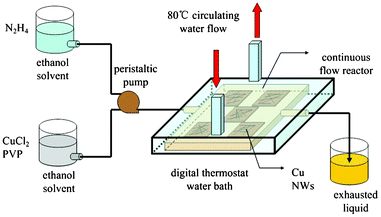 |
| | Scheme 1 Schematic of the CFR for CuNW growth. | |
2.2 Fabrication of CuNW electrode films
For electrode films fabrication, CuNW films were deposited onto clean glass after CFR synthesis process and then treated with poly-L-lysine (Ted Pella). At the same time, poly(3, 4-ethylenedioxythiophene)/poly(styrene-sulfonate) (PEDOT/PSS) aqueous solution (Clevios Al 4083 from H. C. Stark) was deposited on the glass substrate by spin-coating at 2000 rpm. The resulting PEDOT/PSS layer was around 50 nm in thickness. These films were allowed to slowly dry on a shaking plate to prevent wire aggregation. Then, the CuNW/glass was turned side down to face the PEDOT/PSS films. After this step, the CuNWs were transferred onto a 50 nm thick PEDOT/PSS layer spin-coated onto a glass substrate under a heated temperature at 100 °C on the bottom and pressed with a pressure of 0.6 MPa on the top for 20 min (Scheme S1, ESI†).
2.3 Fabrication of glass/CuNWs electrode/P25-TiO2 (N719 dyeing sensitization)/electrolyte/Pt electrode/glass DSSCs
To evaluate the potential use of the fabricated transparent CuNW electrode as a high transparency conducting electrode for DSSC devices, pre-patterned commercial FTO substrates were also used to package FTO-DSSCs for comparison, which were cleaned using the glass clean method described above, including UV-ozone treatment. TiO2 nanoparticles (Degussa P25) were fabricated on pre-treated FTO or CuNW film-coated conducting glass substrates by a screen-printing technique. The dye used in this study was cis-diisothiocyanato-bis(2,2′-bipyridyl-4,4′-dicarboxylato) ruthenium(II) bis(tetra-butylammonium) (N-719, Dyesol) in butanol and acetonitrile (1:1, v/v). Semi-transparent platinum (Pt)-coated glass was used as the counter electrode. An ionic liquid electrolyte containing 0.3 M DMPII, 0.5 M LiI, 0.05 M I2 and 0.5 M 4-TBP in acetonitrile (purchased from HepatChroma SolarTech Co., Ltd) was injected between the two electrodes, driven by capillary force through holes in the hot-melt sealing foil. The ionic liquid possesses high thermal stability, negligible vapor pressure, and low toxicity.
2.4 Characterizations
The powder X-ray diffraction (XRD) patterns were obtained from powder samples mounted on glass slides in a PANalytical D/max-IIIA XRD instrument operating with Cu-Kα radiation (λ = 1.5406 nm). The morphology and elemental composition of the prepared copper nanowires were characterized by scanning electron microscopy (SEM, Netherlands FEI.Co Sirion 200) and energy dispersive X-ray spectroscopy (EDX), respectively. The internal structure and the progress of the synthesis were assessed by transmission electron microscopy (TEM; JEM-2100) performed at an acceleration voltage of 200 kV. Samples were sonicated in ethanol before being dropped on a copper mounted holey carbon film and dried. The statistical characterization of the diameter size distribution of each sample was performed based on the TEM images. Sheet resistance (Rs) of these films was tested by a CheckMate Probe Station CM210 4-point probes resistivity measurement system. The optical transmittance of these films was measured by a U-3900H UV-VIS spectrophotometer. A series of DSSCs were fabricated with traditional sandwich type configuration by using a dye-anchored TiO2 film and a platinum counter electrode deposited on ITO or as-obtained CuNWs film coated conducting glass. A 100 mW cm−2 Xe lamp with an AM 1.5G filter (Sciencetech, Canada) was used as simulation sunlight source. The photovoltaic measurements of DSSCs were recorded by a scanning potentiostat (IVTest Station 2000 Solar Cell I–V Test system, US) and the current–voltage (I–V) curves were measured using a Keithley Model 2400 multisource meter.
3 Results and discussion
3.1 Microstructure characterizations
Typically, 1D CuNWs were obtained by reducing CuCl2·2H2O with hydrazine hydrate through a solvethermal reduction process in the presence of PVP K60, which plays the key role as a structure-directing agent. The color of the solution changed from royal blue to brown after 4 h, indicating the formation of the CuNWs. Compared to our previous work,22 the present process in this study allowed the CuNWs to grow at a lower temperature under 100 °C, resulting in a longer, thinner morphology, and reduced impurities. The morphology and dimensions of the as-prepared CuNWs were investigated by scanning electron microscopy (SEM) as shown in Fig. 1a–c. The CuNWs were straight with diameters in the range of 60–110 nm, and the extraordinary length was over tens micrometers, with an aspect ratio of more than 103. Fig. 1c also shows the tail end of a selected single nanowire, indicating that the nanowires have five side planes forming a pentagonal pyramid tip. The high-resolution TEM (HRTEM) image in Fig. 1e reveals the features of a single-crystal Cu phase. The lattice spacing of the planes perpendicular to the growth direction is 0.209 nm, corresponding to the separation between two (111) planes of face-centered cubic (fcc) copper. The spot feature of selected area electron diffraction (SAED) pattern shown in Fig. 1d, taken along the [110] zone axis perpendicular to the long axis of the corresponding nanowire, also gives evidence for the CuNWs to be single crystalline in nature. The calculated lattice spacing is 2.10 Å which is identical to that of HRTEM observed. Moreover, element and phase analysis of the wires were performed using EDX spectroscopy and XRD. A typical EDX spectrum shows the presence of Cu (8.1 and 8.9 keV) lines (Fig. 1f), which confirms the formation of pure CuNWs. Fig. 1g depicts the XRD pattern of CuNW films drop-casted onto a glass substrate, in which neither a peak proving the presence of a contaminating species nor that of CuO appeared and CuNWs were identified on the basis of the three high angle diffraction peaks that can be indexed as (111), (200) and (220) reflections according to fcc Cu (JCPDS 4-836, a = 3.615 Å).
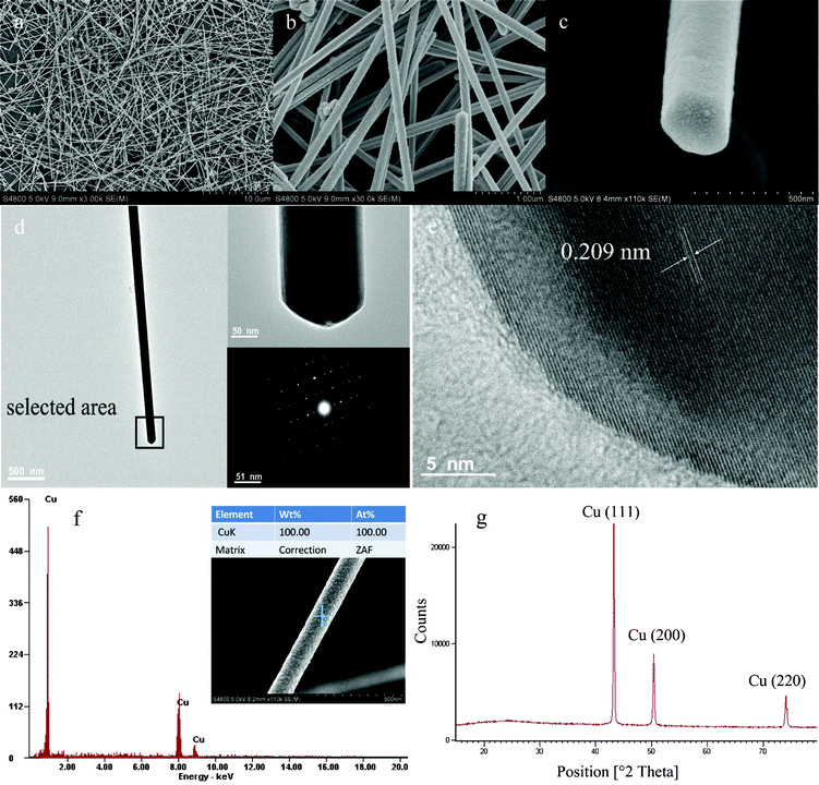 |
| | Fig. 1 (a–c) SEM images of CuNWs at different magnifications, which show ultralong CuNWs with diametersof 60–110 nm and lengths over 30μm. (d) Bright-field TEM image of an individual CuNW (side view), top right inset is high-magnification side view from selected area and the bottom right shows the corresponding SAED pattern which reflects standard fcc-structured copper. e) High-resolution TEM image of an individual CuNW, clearly showing a lattice spacing of 0.209 nm. f) EDX-analysis of a CuNW. g) XRD-pattern of the as-obtained fresh products after drying in an atmosphere of nitrogen. | |
3.2 Growth mechanism
Since the growth mechanism of CuNWs is not yet fully understood, the main reaction taking place to form CuNWs is the reduction of Cu2+ ions (the oxidizing reagent) by the reducing reagent N2H4·H2O which can be represented as eqn (1):| | | 2CuCl2 + N2H4·H2O → 2Cu + N2↑ + 4HCl + H2O | (1) |
For the capping agents/surfactant-assisted wet chemistry method, plenty of surfactants such as PVP in this study have been used to guide the 1D growth of CuNWs. The anisotropic growth of metal crystals is partially ascribed to the selective adsorption of these surfactants onto the specific facet of the nanostructure and leaving the bare facet still active for the further deposition of copper atoms. Additional HRTEM images of seed particles before complete growth reveal that CuNWs are derived from multiply-twinned particles (MTPs), which could be a clue to their origins. As observed in Fig. 2, it is concluded that the anisotropic growth of MTPs is realized by selectively covering the facets {100} with PVP so that they are completely passivated, while the {111} facets at the ends of the nanostructures are largely bare and still quite active. Hence, the reduced copper atoms are preferentially deposited onto {111} facets, leading to the anisotropic growth of CuNWs. Furthermore, we have also found another interesting feature from the HRTEM of this penta-twinned crystal with 5-fold axis—that the theoretical interfacial angle between two {111} facets on the top surface was just 360°/5 = 72°, while actually the angles between the twin boundaries tend to be 70.5° for a perfect fcc crystallite, deviating 0.4–3.0° from the ideal fcc crystal prescribed angle. This data is clear verification that there must be a lattice distortion in the real CuNW crystal and that the atoms surrounding the radial direction are shared irregularly between the five twin-boundaries by crystal strain and dislocation so as to form seamless NWs. This experimental discovery is similar to that reported by Jin et al.,16 who also reported that the solution growth of CuNWs is driven by screw dislocations. Although surfactant-based techniques are very successful and powerful for the fabrication of a large variety of NWs, this method fails to produce nanostructures with feature sizes smaller than 40 nm, owing to a limit of the molecular sizes of capping agents and the stability of the crystal structure in the solution system.
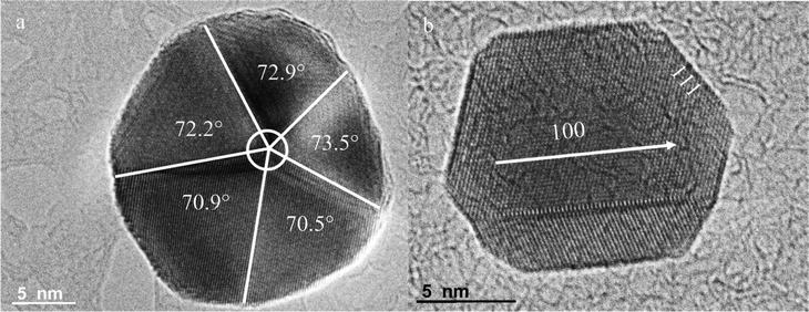 |
| | Fig. 2 a) HRTEM image of Cu multiply-twinned particles (top view) synthesized for 0.5 h by an interrupting growth process, revealing the angles between the {111} planes of the subcrystals. b) The HRTEM image illustrated circumstantial evidence of the pentagonal model for CuNW growth from MTPS, in which the nanoparticle was synthesized for 0.7 h. | |
Previously, we reported that the morphology and the aspect ratio of the nanowires were found to be related to the molar ratio of surfactant to copper source as evidenced by SEM.22 In this case, it also can be seen that the products are not uniform in size and shape and that many irregular particles appear in the products when excess PVP was used. Upon increasing the concentration ratio of PVP to copper chloride from 1 to 4, more and more nanoparticles of almost spherical shape appeared in the SEM images (as shown in Fig. S1, ESI†). Now we could understand that PVP is one of the key parameters determining the final shape of crystallographic structure of the seeds in the nucleation process and in the following stages of growth. In addition, the strong reducing agent N2H4·H2O plays another significant role in the reaction. According to eqn (1), it is easy to know that hydrazine hydrate disturbs the stability of the pH environment as the redox reaction progresses due to HCl by-products that lower the redox over-potential and crystal growth supersaturation. Moreover, HCl can also accumulate in the system and, at certain levels, prove surface corrosion and poor dispersion for the CuNWs (Fig. S2, ESI†). Thus, a CFR was then employed to solve the precursor depletion and accumulation of coproducts problem. Precursor solutions of the same concentration of each component at stable pH conditions were flowed through the CFR to produce NW products with longer lengths and uniform diameters. Besides, in an effort to achieve a suitable pH environment and further lower the supersaturation of the system—which intrinsically promotes the efficiency of the reaction, we also changed the solvent from ethanol to distilled water and added a suitable amount of strong complexing ligand, ammonia, which is capable of complexing with Cu2+ to form Cu(NH3)4(OH)2. Interestingly, HRTEM studies have shown that CuNWs suspended in aqueous solution were readily oxidized to Cu2O nanocrystals by dissolved oxygen, and many oxide pit layers were observed along the CuNWs (Fig. 3, S4, ESI†). The two different lattice spacings of 0.21 and 0.25 nm correspond to the separation between the two (111) planes of fcc copper and (110) planes of cubic Cu2O, respectively. The SAED of a NW (Fig. 3a) also shows the NW to be single-crystalline yet with extra diffraction spots that can be indexed to Cu2O (JCPDS 5-667, a = 4.270 Å). In addition, the surface information of the freshly obtained sample using aqueous solution as shown in Fig. 4a can be properly provided by XPS analysis. The binding energies obtained in XPS analysis were corrected with the reference to C1s (284.6 eV) and illustrate the existence of cuprite Cu2O on the basis of an analysis for the binding energies of Cu 2p3/2 (932.4 eV for Cu0 and 932.2 eV for Cu+) and the main O 1s (530.6 eV for the anion O2− in the cuprite; reference O 1s for Cu2O and CuO are 530.4 and 529.6 eV, respectively). Thus the composition of the oxides layers can be determined to be mainly the Cu2O phase, which in good agreement with the result from XRD (Fig. 4b). In brief, we selected the strong chemical reduction of Cu(II) in ethanol rather than in water to prepare well-crystallized CuNWs, which results in better stability and retention of the smooth surface after storage. This process is safe, easily-controlled and can be scaled up by increasing the number of glass substrates. According to practical experience, we could obtain 0.42 g CuNWs (drying with nitrogen gas) after the whole process finished (4 h) when we used 5 growth substrates (2.0 cm × 2.0 cm × 2.2 mm), which means 0.105 g h−1. However, this is not a maximum result. Obviously, there is more product available if we increase the number of substrates or enlarge the growth area of a single substrate. This result implies that the fabrication of the CuNW membrane can be extended to a large area through continuous processing, which could help to realize a low-cost and flexible transparent electrode for applications in solar cells.
![HRTEM image of a CuNW prepared within different solvent systems: a) water, b) ethanol. Insets are the corresponding SAED patterns, taken along the [110] zone axis perpendicular to the long axis of the nanowire.](/image/article/2012/RA/c2ra21224b/c2ra21224b-f3.gif) |
| | Fig. 3 HRTEM image of a CuNW prepared within different solvent systems: a) water, b) ethanol. Insets are the corresponding SAED patterns, taken along the [110] zone axis perpendicular to the long axis of the nanowire. | |
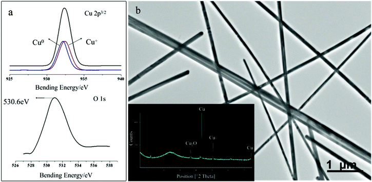 |
| | Fig. 4 a) XPS spectra of Cu 2p3/2 and O 1s photoelectrons of CuNWs prepared by a hydrothermal process in aqueous solution. b) TEM image of samples fabricated at 80 °C for 4 h (inset is corresponding XRD patterns). | |
3.3 Characteristics of the transparent Cu electrode films
As seen in the SEM image shown in Fig. 5a, networks of NW membranes fabricated for 4 h with some big holes that are above percolation and their density of NWs are calculated as a function of solvothermal deposition times. A four-probe method was used in sheet resistance measurements in order to avoid contact resistance between test electrodes and CuNWs membrane, and the I–V curves of the nanofiber network are linear, indicating excellent ohmic transport in the transparent CuNWs membrane (Fig. 5b). The uniformity of the transparent electrode across the 1 × 1 cm sample was measured, whose Rs is 13.7 Ω sq−1, similar with that of the FTO (15 Ω sq−1, on 2.2 mm glass purchased from NSG, Japan) we used in this study, and the result implies that the coalition of solvothermal and polymer spin processes can be used for fabrication of transparent electrodes with excellent film uniformity. The simulated sunlight optical transmittance of the 4 h fabricated 1 × 1 cm CuNW membrane electrode after PEDOT/PSS spining on a 2.0 cm × 2.0 cm × 2.2 mm glass substrate in the visible wavelength range was measured and is shown in Fig. 5c. FTO has a peak transmittance of 85% at 550 and 750 nm, and an average transmittance of 81% in the whole visible range. By comparison, the CuNWs membrane shows an excellent, flat spectrum over the entire visible range from 400 to 900 nm and the average transmittance is about 80%, which can remove excess process steps and color adjustment components. Meanwhile, both the sheet resistance and the transmittance decrease dramatically as the density of the CuNWs increases with increasing deposition time during the solvothermal reduction process. Typically, 150 Ω sq−1 at 90%, 70 Ω sq−1 at 85%, and 12 Ω sq−1 at 78% can be realized for 3.6, 4.4 and 4.8 h syntheses, respectively. Thus, it is shown that optical transparency and electrical conductivity can be controlled by the densities of NWs within the membrane, providing sufficient design latitude for optimal performance. More interestingly, we also found that the increase in the transmittance by reducing the NW diameter is also accompanied by an increase in sheet resistance through changing the concentration of PVP during our synthesis process. To characterize the optical transmittance and sheet resistance of the CuNW membrane, four sets of samples (main average diameter: 350, 200, 110, 80 nm, corresponding PVP concentration: 0.9, 0.7, 0.5 and 0.4 mM, respectively) were prepared. Fig. 5d shows the average transmittance and sheet resistance for CuNW membranes with different diameters. For this considered case, the sheet resistance can be decreased by more than 65% but the transmittance is decreased by less than 19% using thicker CuNWs from 80 to 350 nm (note that the decrease of light tansmission is not only due to CuNW diffusion to the surface of the polymer layer but also NW purity in the final products, which plays a more significant role in impeding the transparent performance, confirming that NPs possesses a high capacity to collect holes). An important point can be made from these results: that the transparency of such an electrode structure can be increased without sacrificing the overall conductivity by using narrower and thicker NWs, if purity can be further improved during thicker NWs synthesis. This characteristic is another advantage over TCO electrodes in which the sheet resistance has to be compromised in order to achieve high transmittance. Therefore, CuNW transparent metal electrodes are very promising not only because they can prevent the disadvantages of FTO electrodes but also because they can meet the requirements of both sheet resistance and optical transmittance by optimizing the synthesis process.
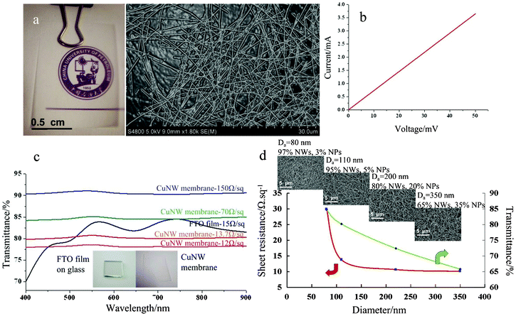 |
| | Fig. 5 a) Digital photo of a typical transparent CuNW membrane with specific density synthesized for 4 h during solvothermal process. The right column shows the corresponding SEM images. b) I–V curve of CuNW membrane with a transparency of 80%; the tested sample has a size of 1 × 1 cm. c) Optical transmittance spectrum of CuNW membrane with different sheet resistances and FTO on glass. The spectra for CuNW membranes are much flatter than that of FTO film. Inset: photograph of the flexible CuNW membrane and the commercial FTO electrode on glass. d) Average transmittance and sheet resistance of various CuNW diameters, (insets are the corresponding SEM images of samples with different nanowire diameters and final nanostructures prepared in the presence of a series of PVP concentrations. Scale bar is 5 μm, NPs means nanoparticles and Da means average diameter). | |
To evaluate the potential of transparent CuNW membranes used in solar cell applications, DSSCs were fabricated onto transparent CuNWs electrodes with T = 80% and Rs = 13.7 Ω sq−1 on glass with the structure of glass/CuNWs/P25-TiO2(N719)/electrolyte/Pt/glass. The fabrication is described in the experimental section, and the solar cell is shown schematically in Fig. 6a. The presence of the transparent, conductive PEDOT/PSS layer ensures that holes generated in the solar cell are collected efficiently despite the relatively large distance between the CuNWs compared to the thickness of the organic layers. This percolation problem, which could be detrimental to some electrode applications, can also be overcome effectively by incorporating other materials into CuNW networks, such as CNTs and graphenes.23–25 For comparison, cells were also formed on SnO2/F glass (FTO) as front contact electrodes with the same structure. The current density (J) versus voltage (V) characteristics were measured in air by illuminating the DSSC devices with AM 1.5G simulated sun light (Oriel Solar Simulator, 100 mW cm−2). Similar to the FTO system, the transparent CuNW membrane electrode also shows higher power conversion efficiency than specular transmittances, indicating that such electrodes are interchangeable (Fig. 6b). The power conversion efficiency of the device is 5.0%, which is comparable to devices made on glass/FTO substrates (4.8%). The figures of merit for the device using a glass/Cu membrane substrate (Jsc 20.61 mA cm−2, Voc 0.63 V, FF 0.37) are comparable to a device using glass/FTO as the substrate (Jsc 20.65 mA cm−2, Voc 0.62V, FF 0.35) with the exception of the lower fill factor (FF). The slightly lower Jsc of the Cu device can be attributed to the lower transmittance of the Cu mesh electrode at the light absorption range of the active layer than that of the FTO electrode. Additionally, it is well known that the light scattering effect can be improved by employing large-sized scatterers, however, for a given scatterer size, the large scattering of the metal NWs can enhance the solar cell performance due to an effective increase in the light absorption path length in the active layer. Thus, the efficiency of the cells with CuNWs was a little higher than that of the cell with the FTO.
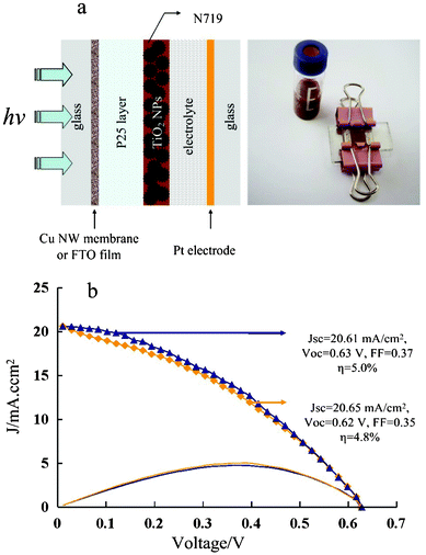 |
| | Fig. 6 a) The schematic DSSC and the band structure of glass/CuNW membrane/P25-TiO2 (N719)/electrolyte/Pt/glass. The right column shows the corresponding digital photo of theDSSC device and CuNWs products dissolved in ethanol. b) Photocurrents as a function of photovoltage for DSSCs assembled with transparent CuNW membrane on glass substrate (△) and FTO film on glass substrate (◇) under AM 1.5G conditions. | |
Conclusions
In summary, we have demonstrated a simple, rapid, and low-cost solvothermal method to fabricate ultra-long, single-crystal CuNWs and transparent CuNW membranes under mild conditions. These electrodes are fabricated entirely from solution and require only a low temperature annealing step. These as-prepared NW networks are excellent transparent electrode materials, with performances comparable to the commercial transparent electrodes in terms of transmittance and sheet resistance but much cheaper. Furthermore, we have developed DSSCs with 1D CuNWs for the improvement of solar cells. The short-circuit current density of the cell reached 20.61 mA cm−2, and the photovoltaic efficiency was upto 5.0%, which is approximate to that of the device with the FTO electrode. It is believed that such electrode structures may continue to expand and open up new applications, such as transparent electrodes, for organic solar cells, flexible OLED displays, and screen applications etc.
Acknowledgements
This work was supported financially by the National Natural Science Foundation of China (Grant No. 50901090).
References
- Y. Zhou, S. Sreekala, P. M. Ajayan and S. K. Nayak, J. Phys.: Condens. Matter, 2008, 20, 095209 CrossRef.
- Cheng He, Wenxue Zhang and Juanli Deng, J. Phys. Chem. C, 2011, 115, 3327–3331 CAS.
- Weihong Xu, Yongxing Zhang, Zheng Guo, Xing Chen, Jinhuai Liu, Xingjiu Huang and Shu-Hong Yu, Small, 2012, 8(1), 53–58 CrossRef CAS.
- Yang Liu, Zhen Liu, Ning Lu, Elisabeth Preiss, Selcuk Poyraz, M. J. Kim and Xinyu Zhang, Chem. Commun., 2012, 48, 2621–2623 RSC.
- Yanhu Wei, Steven Chen, Bartlomiej Kowalczyk, Sabil Huda, T. P. Gray and B. A. Grzybowski, J. Phys. Chem. C, 2010, 114, 15612–15616 CAS.
-
(a) A. R. Rathmell, S. M. Bergin, Yi-Lei Hua, Zhi-Yuan Li and B. J. Wiley, Adv. Mater., 2010, 22, 3558–3563 CrossRef CAS;
(b) R. R. Aaron and J. W. Benjamin, Adv. Mater., 2011, 23, 4798–4803 CrossRef.
- Hui Wu, Liangbing Hu, M. W. Rowell, Desheng Kong, J. J. Cha, J. R. McDonough, Jia Zhu, Yuan Yang, M. D. McGehee and Yi Cui, Nano Lett., 2010, 10, 4242–4248 CrossRef CAS.
- Jun Liang, Hui Bi, Dongyun Wan and Fuqiang Huang, Adv. Funct. Mater., 2012, 22(6), 1267–1271 CrossRef CAS.
- Myung-Gyu Kang, Hui Joon Park, Se Hyun Ahn and L. Jay Guo, Sol. Energy Mater. Sol. Cells, 2010, 94, 1179–1184 CrossRef CAS.
-
(a) Hyungsoo Choi and Sung-Ho Park, J. Am. Chem. Soc., 2004, 126, 6248–6249 CrossRef CAS;
(b) Changwook Kim, Wenhua Gu, Martha Briceno, I. M. Robertson, Hyungsoo Choi and Kyekyoon (Kevin) Kim, Adv. Mater., 2008, 20, 1859–1863 CrossRef CAS.
- Ying Zhang, Frank Leung-Yuk Lam, Xijun Hu, Zifeng Yan and Ping Sheng, J. Phys. Chem. C, 2007, 111, 12536–12541 CAS.
- Zhaoping Liu, You Yang, Jianbo Liang, Zhaokang Hu, Shu Li, Sheng Peng and Yitai Qian, J. Phys. Chem. B, 2003, 107, 12658–12661 CrossRef CAS.
- Yu Chang, Mei Ling Lye and Hua Chun Zeng, Langmuir, 2005, 21, 3746–3748 CrossRef CAS.
- Bin Deng, An-Wu Xu, Guang-Yi Chen, Rui-Qi Song and Liuping Chen, J. Phys. Chem. B, 2006, 110, 11711–11716 CrossRef CAS.
- Melinda Mohl, Peter Pusztai, Akos Kukovecz and Zoltan Konya, Langmuir, 2010, 26(21), 16496–16502 CrossRef CAS.
- Fei Meng and Song Jin, Nano Lett., 2012, 12, 234–239 CrossRef CAS.
-
(a) X. Y. Tao, X. B. Zhang, J. P. Cheng, Z. Q. Luo, S. M. Zhou and F. Liu, Diamond Relat. Mater., 2006, 15, 1271–1275 CrossRef CAS;
(b) Lixin Dong, Xinyong Tao, Li Zhang, Xiaobin Zhang and B. J. Nelson, Nano Lett., 2007, 7(1), 58–63 CrossRef CAS.
- Fung Suong Ou, M. M. Shaijumon, Lijie Ci, Derek Benicewicz and Robert Vajtai, Appl. Phys. Lett., 2006, 89, 243122 CrossRef.
- Q. Zhang, W. Z. Qian, H. Yu, F. Wei and Q. Wen, Appl. Phys. A: Mater. Sci. Process., 2007, 86, 265–269 CrossRef CAS.
- F. Kokai, T. Shimazu, K. Adachi, A. Koshio and Y. Takahashi, Appl. Phys. A: Mater. Sci. Process., 2009, 97, 55–62 CrossRef CAS.
-
(a) A. G. Genaro, Z. T. M. Murakami, M. J. Krantz and J. A. Haber, J. Mater. Chem., 2006, 16, 3075–3083 RSC;
(b) A. G. Genaro, Bin Lin, Uttandaraman Sundararaj and J. A. Haber, Adv. Funct. Mater., 2006, 16, 2423–2430 CrossRef.
- Yuxin Zhao, Ying Zhang, Yanpeng Li and Zifeng Yan, New J. Chem., 2012, 36, 130–138 RSC.
- Shisheng Li, Yanhong Luo, Wei Lv, Wanjing Yu, Sida Wu, Pengxiang Hou, Quanhong Yang, Qingbo Meng, Chang Liu and Hui-Ming Cheng, Adv. Energy Mater., 2011, 1, 486–490 CrossRef CAS.
- Xiangjian Wan, Guankui Long, Lu Huang and Yongsheng Chen, Adv. Mater., 2011, 23, 5342–5358 CrossRef CAS.
- D. S. Hecht, Liangbing Hu and Glen Irvin, Adv. Mater., 2011, 23, 1482–1513 CrossRef CAS.
Footnote |
| † Electronic Supplementary Information (ESI) available. See DOI: 10.1039/c2ra21224b |
|
| This journal is © The Royal Society of Chemistry 2012 |
Click here to see how this site uses Cookies. View our privacy policy here.