DOI:
10.1039/C2RA22280A
(Paper)
RSC Adv., 2012,
2, 11359-11365
Microscopy study of snail trail phenomenon on photovoltaic modules
Received
25th September 2012
, Accepted 25th September 2012
First published on 27th September 2012
Abstract
Snail trails on photovoltaic modules are a source of enormous concern to the solar industry as no scientific reports on the mechanisms producing this global phenomenon were previously available. Here, for the first time, we clarify the origin of these snail trails as a product of the formation of silver carbonate nanoparticles which discolor the silver grid. Micropore arrays on the silicon substrate within the snail trail region could accelerate the discoloration by offering reactive compounds via penetration and release. The potential mechanisms of photovoltaic module discoloration are proposed, yielding clues as to how snail trail formation can be mitigated by technical solutions. Aging tests on the discolored modules suggest no significant power degradation or discolored area enlargement after accelerated aging.
1 Introduction
Projections of the world’s energy needs leading up to 2050 suggest an increase in the demand (to the order of 1 GW day−1) that will be proportionate to the growing instability of the energy supply.1 Finite supplies of fossil fuels will eventually be depleted while introducing enormous environmental concerns. Public and regulatory anxiety surrounding nuclear energy has increased since the Fukushima nuclear plant disaster, resulting in some EU member states reducing their dependence on nuclear sources. Consequently, the development of alternative safe and “renewable” energy sources with low-carbon emissions is essential to fill projected energy shortfalls. Solar energies (thermal and electric) are truly renewable, leading to great interest from regulators, investors, and the general public.
Recent advances in photovoltaic (PV) technology have delivered an efficient means of harvesting solar energy with the advantages of being a silent technology with no moving parts, which in principle, requires little or no maintenance once installed.1,2 Solid state junction solar cells exploit PV technology to convert incident sunlight directly to electricity using crystalline and amorphous silicon (Si),3,4 copper–indium–gallium–selenide,5–7 cadmium telluride8 and other thin films.9 Other hybrid junction solar cells, such as polymer and organic–inorganic hybrid assemblies, have also drawn much attention.10 However, due to the rare element usage and inherent toxicity of Cd, Te, Ga, and Se in solid state junction devices,11–13 these newly developed hybrid junction solar cells are still in their infancy, currently yielding only low efficiencies, resulting in the domination of the solar industry by crystalline Si solar cells. Many jurisdictions in Europe, America and Asia have introduced subsidies to encourage the installation of Si solar cells to diversify and optimize the energy supply infrastructure. Although Si solar cell technology is maturing after decades of development, new challenges have arisen, such as the need to increase efficiency while lowering the cost of mono- and polycrystalline Si manufacturing as well as the degradation of PV modules after installation.14–16 Some forms of degradation are due to the different working conditions, such as the solar light intensity, and climatic conditions. However, in the last three years, an emerging widespread phenomenon called ‘snail trails’, small, dark lines or partial cell-discolorations on PV modules, has drawn considerable attention in the solar industry.17 Many manufacturers have begun investigating the exact causes of snail trails and the reliability and efficiency of PV modules after discoloration. Fortunately, snail trails appear to have a minimal effect on the PV module efficiency (Fig. 1), with an average power degradation of 1.4% (eff.% dropped 0.34%) in discolored PV modules (on average power degraded by 0.56% yearly after subtracting the initial light-induced degradation, which is considered to be in the normal degradation range for p-type technology after installation). If subtle alterations in the performance and appearance of PV modules by snail trails are the most obvious short-term symptoms, there could be additional longer-term negative influences on the product lifespan. Consequently, it is of great research interest to elucidate the mechanisms generating snail trails and their contributions to the discoloration of PV modules.
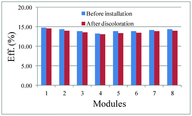 |
| | Fig. 1 Efficiency changes before installation and after discoloration (data from Canadian Solar Inc.) | |
For the first time, we present herein the origins of these snail trails on PV modules, with the identity of the chemical likely responsible for the discoloration confirmed. Further, the mechanisms underlying the discoloration are discussed, providing insights for both researchers and manufacturers to address this issue and minimize losses incurred by the generation of snail trails within the solar industry.
2 Experimental
PV modules displaying snail trails were collected from their previous field deployments and dissembled to access the discolored Si cells. The encapsulation layers (cured ethylene vinyl acetate, EVA) were mechanically removed at room temperature to avoid oxidation of the cells caused by heating. Small pieces (∼5 mm2) of solar cells with silver grids were taken from the affected “snail trail” as well as non-affected “normal” regions. More than five PV modules (modules with different snail trail features from Canadian Solar Inc.) were investigated to characterize the discoloration.
Electroluminescence (EL) analysis and infrared (IR) measurements were taken by an EL camera (PCO-Edge) and IR scanner (Fluke Ti32). Optical (Olympus BX 51 M) and field-emission scanning electron microscopy (FE-SEM, ZEISS LEO 1530) were used to study the topical surface microstructure of both the discolored and normal regions of the solar cells. Energy-dispersive X-ray spectroscopy (EDS, EDAX Pegasus 1200) was employed for elemental analysis. Raman spectra of the discolored and normal regions of the cells were measured with a Renishaw micro-Raman spectrometer with 1.5 mW of laser radiation at an excitation wavelength of 488 nm. A 50× objective was used with a focal spot of about 5 μm and a spectral resolution of 1 cm−1. X-ray photoelectron spectroscopy (XPS, PHI Quantera, ULVAC-PHI) was employed to study the surface chemistry. Discolored samples were cut by an ultrathin blade and focused ion beam (FIB, ZEISS Nvision 40 FIB/FE-SEM) for high resolution transmission electron microscopy (HRTEM, JEOL 2010F) observation.
3 Results and discussion
3.1 Discoloration on Ag grids
An optical photograph and corresponding electroluminescence and infrared images of PV modules with snail trails are shown in Fig. 2. These snail trails were randomly located and oriented on the module, without any defining shape or pattern (Fig. 2a) and were spatially-correlated with dark areas on the electroluminescence image (note: high magnification images, inset Fig. 2b). Infrared temperature mapping (Fig. 2c) shows that the temperature of the snail trail-affected regions of the solar cells is usually lower than that of its adjacent non-affected “normal” regions. From the latter analysis, it can be seen that these low temperature regimes can be attributed to low local current densities. Those lowest temperature regions (green color labeled in Fig. 2c) without snail trail features display clear cracks, except at the edge of the modules. Hence the cracked area displays a low temperature due to the open circuit, while the edge area presents a low temperature due to the heating sink effect. The lower temperatures in the snail trail affected areas (corresponding to dark areas on the electroluminescence image) indicate that there was no short-circuiting on the discolored PV modules during operation. Collectively, these measurements suggest that there were both color changes on the silver grids overlaid by snail trails, and some random underlying micro-defects on the SiN film or the Si substrate according to EL images (as will be discussed subsequently in more detail). It is worth noting that these snail trails appear on both the edge and centre areas of the cells without any connections, however, they usually develop along cracks or the edges of cells.17
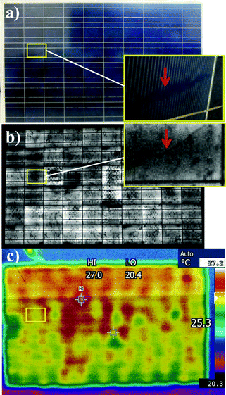 |
| | Fig. 2 Optical, electroluminescence (EL) analysis, and infrared (IR) measurement images of the discolored module. | |
Microstructural analysis of the discolored Ag grids revealed that a considerable number of nanoparticles, of less than 30 nm, were observed in the affected “snail trail” regions relative to the “normal” regions on the same solar cell (Fig. 3). Comparing the inset optical images of Fig. 3a and c, the dark color of the Ag grids are significant in the snail trail regions. In the high magnification SEM images, Fig. 3b and d, the only prominent distinction for the darker grids exists on the Ag surface, comprising numerous nanoparticles. It is well accepted that the presence of nanoparticles will often darken a material as they can scatter and, more specifically, absorb a wide range of visible light wavelengths.18–22 Consequently, nanoparticles present on Ag grids could enhance light absorption and scattering due to size effects and give incrementally darker coloration than normal grids that are free of nanoparticles. It is worth mentioning that there were also some larger particles located on the Ag grain boundary regions, with EDS element mapping indicating that they are ZnO (Fig. 4). These ZnO particles, an inorganic glass binder coming from the Ag paste manufacturing,23–25 could have nucleated and crystallized on the grain boundary due to its high surface energy during the sintering of the Ag paste for forming the grids. Considering that these ZnO particles are found in both discolored and normal regions, it is unlikely that they contribute significantly to the snail trail solar cell discoloration.
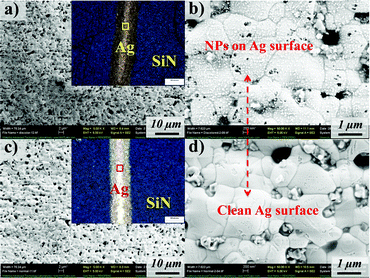 |
| | Fig. 3 SEM images of the discolored grid at (a) low and (b) high magnification; and normal grid at (c) low and (d) high magnification. (Insets are the corresponding optical images of the Ag grids and SiN films from the snail trail and normal regions.) | |
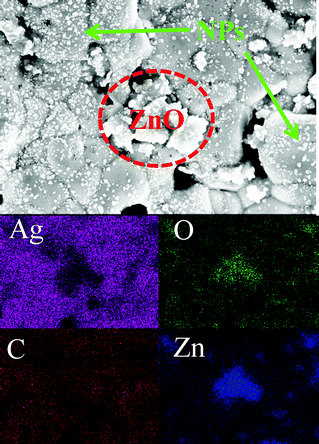 |
| | Fig. 4 EDS elements mapping on the discolored grid. | |
To investigate changes in the surface chemical composition of the Ag grids, micro-Raman and XPS were employed. The Raman spectra of the SiN film and Ag grid are shown in Fig. 5. There were no evident changes in the Si substrates (Fig. 5a), while the carbon-related peaks changed significantly in the discolored relative to normal Ag grids (Fig. 5b). The strong vibrations ν1, ν3 and ν4 of CO32− at 1047 cm−1, 1440 cm−1 and 722 cm−1 Raman wavelengths, respectively, were observed for the discolored Ag grids, while only a low intensity of these bands were found for the normal Ag grids, which confirms the previous results on calcium carbonate, artinite and calcite.26–28 The Raman shifts at 480, 570 and 960 cm−1 can be identified as the Ag–O stretching vibration bands. The peaks at 1350 and 1520 cm−1 correspond to the symmetric and asymmetric stretching of O–C–O.29 Acetate groups from the EVA encapsulation layer have also been detected at 1150 cm−1.30,31 As shown in Fig. 6, the XPS peaks of the normal and discolored Ag grids, located at 367.8 eV (Ag 3d 3/2), 373.8 eV (Ag 3d 5/2), 285.5/290 eV (C 1s) and 533.3 eV (O 1s), correspond to Ag2CO3.32,33 The slight shifting of these peaks can be attributed to the changed conductivity of the samples. Compared to pure Ag, the normal and discolored Ag grids displayed stronger C 1s and O 1s peaks because of the higher C and O content in the grids. However, the result did not indicate any significant differences between the normal and discolored grids. This is because of the influence of the residual EVA on the surface of the Ag grids originating from sealed cells. The residual EVA is also evident in the Raman results (as shown in Fig. 5). We tried to remove the EVA by chemical solvents, heating or sonication. All of these attempts resulted in dramatic surface structure modifications and damaging of the embedding structure of the nanoparticles. This indicates that the XPS measurement is not suitable to identify the C origins. Moreover, there were no S or Cl related peaks observed in the Raman and XPS results, indicating that the discoloration was not due to AgCl or Ag2S, but to carbon and oxygen related Ag component formation in the darkened regions of the Ag surfaces. Because the Zn 2p peaks were weak and difficult to identify from background, ZnO, as a key compound accounting for the discoloration, can be ruled out.
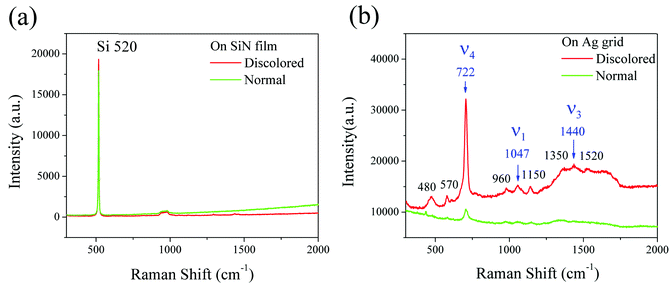 |
| | Fig. 5 Raman spectra of the discolored and normal regions on the (a) SiN film and (b) silver grid. | |
 |
| | Fig. 6 XPS of (a) Ag3d, (b) C1s and (c) O1s for the discolored and normal Ag grids. | |
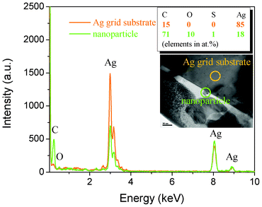
To identify the nanoparticle components of the discolored regions in an Ag grid (Fig. 3b), FIB was employed to prepare samples for TEM analysis. First, a layer of tungsten was deposited on the discolored Ag grid surfaces to protect the nanoparticles from damage during sample processing. Subsequently, two grooves were cut and a thin slice was formed (Fig. 7a) and excised prior to reduction to a 100 nm thickness for HRTEM observation (Fig. 7b), where the nanoparticles were clearly visible on the Ag grid surface (inset TEM Fig. 8). The EDS results indicate that C and O atomic ratios on the nanoparticle increased while Ag decreased relative to the ratios on the Ag grid (inset table in Fig. 8). S, originating from the Ag paste or EVA layer, only changed by 1%, suggesting that S has little relationship with the solar cell discoloration, a result that is consistent with that obtained by XPS.
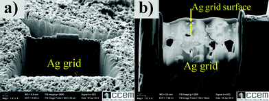 |
| | Fig. 7 FIB of the discolored Ag grid. (a) Overview of FIB section (5 μm × 10 μm) on the discolored Ag grid and (b) ultrathin slice (∼100 nm) of the discolored Ag grid for TEM observation. | |
The TEM images of the FIB sample taken from the discolored Ag grid surface illustrate that some nanoparticles are present between the tungsten layer and the Ag grid substrate (Fig. 9a and the corresponding high resolution image Fig. 9b, measured at a lattice distance of 2.37 Å). Nanoparticles scratched from the discolored grid regions were mainly polycrystalline and less than 30 nm, which is consistent with SEM observations (Fig. 9c and d, one lattice distance is 2.04 Å). We compared the measured lattice distances using HRTEM to serial the crystalline data from the standard database of the Powder Diffraction File (PDF). We then identified the appropriate chemical phases and crystal structures. These lattice distances were well matched with those of Ag2CO3 and confirmed that the nanoparticles on the discolored Ag grid surfaces were Ag2CO3. All measured lattice distances (mld) and the calculated lattice distances (cld) of Ag2CO3 from the standard database [PDF 70-2184 (ref. 34)] are listed in Table 1.
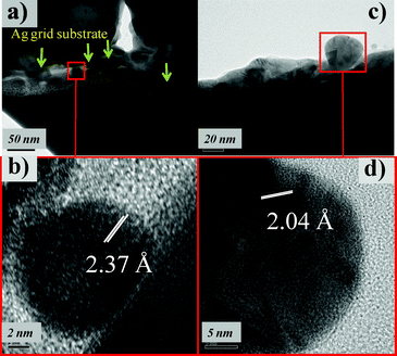 |
| | Fig. 9 TEM of (a, b) the FIB sample and (c, d) the scratched sample. | |
Table 1 Measured d value of the nanoparticles and the corresponding crystal planes of Ag2CO3
| mlda |
2.54 |
2.42 |
2.39 |
2.37 |
2.35 |
2.29 |
2.32 |
2.13 |
2.09 |
2.04 |
|
The mld values were the measured d value in angstroms. The cld and hkl values were taken from PDF 70–2184 (Ag2CO3).
|
| cld |
2.56 |
2.42 |
2.39 |
2.38 |
2.35 |
2.28 |
2.32 |
2.14 |
2.08 |
2.04 |
|
hkl
|
111 |
200 |
040 |
−121 |
210 |
031 |
121 |
140 |
−131 |
131 |
3.2 Microstructures on the SiN film and Si substrate
The morphology of the SiN films and the Si substrates taken from the discolored and normal regions (Fig. 10) reveals the presence of fine black lines (both under electron beam and visible light, see SEM and inset optical micrographs of Fig. 10a) which are not micro-cracks but micropore arrays with line separation distances of 1–100 μm and closed pores of 1–2 μm in diameter (as highlighted by the circle and inset illustrated in Fig. 10b). Such micropore arrays, which are widespread in the discolored regions, could be formed during the texturization process of the Si substrate manufacturing. Conversely, relatively few micropore arrays and smaller micropores were observed on the SiN films in the normal regions (Fig. 10 c and d). These micropore arrays could appear as dark areas under EL testing due to low electron densities in these regions (Fig. 2b). We speculate that these micropore arrays also discolor the modules on SiN films by trapping light and thereby producing a dark appearance to the naked eye as highlighted by the arrow in the inset optical micrograph in Fig. 10a, contributing to the “snail trail” darkened appearance.
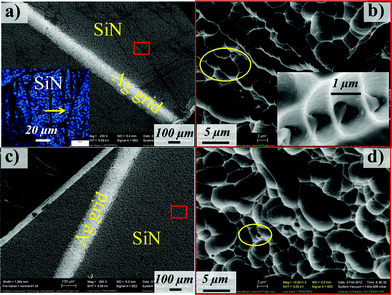 |
| | Fig. 10 SEM images of (a) the discolored SiN film (inset: the optical micrograph of the SiN film) and (b) high magnification of the red box (inset: the detailed micro-defects). (c) Normal grid and (d) high magnification image. (Circles highlight the micropores.) | |
3.3 Mechanism of Ag2CO3 formation
It is worth noting that the micropore arrays mentioned in the previous section may provide potential channels allowing Ag grids access to oxygen, carbon dioxide, water and other reactive compounds, which could oxidize Ag directly or accelerate this process. These compounds could also be sealed in the micropores during fabrication and released slowly during module operation. Oxidation of Ag and the reaction with CO2 accounts for the formation of Ag2CO3 nanoparticles and eventually leads to the snail trails on PV modules. This mechanism for PV module discoloration is schematically shown in Fig. 11. The porous surface and embedding nanoparticles certainly increased the resistance. At a constant potential these areas would carry a low current density and thereby display a low temperature as shown in Fig. 2c.
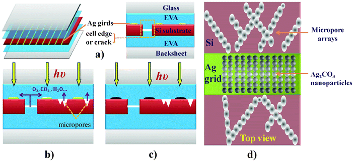 |
| | Fig. 11 Mechanism of discoloration: (a) scheme of PV module; (b) reaction chemical penetration or release; (c) Ag2CO3 formation and Ag grid discoloration; (d) zoom in of the top view of the snail trail region, Ag2CO3 NPs on the Ag grid and micropore arrays on the SiN film. Please note that there is a thin SiN layer on Si wafer. | |
The structure of PV modules (Fig. 11a) is permeable to some extent to moisture and atmospheric gases due to the nature of the EVA layers and backsheet; however, the presence of micropores, gaps between cells (edges) or cracks on the Si substrates could allow oxygen, carbon dioxide, water or other reactive compounds, which may come from aged EVA, silver paste or the open environment, to more readily propagate along these micro-channels from the backsheets or to be sealed in the micropores and slowly released during module operation (Fig. 11b). Consequently, these reactive compounds could directly oxidize Ag to form Ag2CO3 nanoparticles, with water, ultraviolet light exposure, electrical current, and heat accelerating oxidation of the Ag grid (Fig. 11c). Therein, the discoloration of PV modules contains two parts: one is from the Ag2CO3 nanoparticles on the Ag grids and another is from the micropore arrays in the correlated areas between the discolored Ag grids on the SiN films, as shown in Fig. 11d. Usually, the widths of the micropore arrays are in the micro range, a size which could not be distinguished by the naked eye (general dimension is ∼100 μm with 0.6 m viewing distance for the naked eye). Hence, the dark appearances from the Ag2CO3 nanoparticles on the Ag grids and the micropore arrays on the SiN film are integrated together because of their correlations as discussed previously, displaying those “continuous” discolored grids and substrates – like “snail trails”.
3.4 Reliability test of the discolored PV modules
Based on our studies, Ag2CO3 nanoparticles appear only at the interface between the Ag grids and the EVA layer. They do not appear in the anti-reflection coating area of cells, nor do they occur on top of the ribbons. The very small physical size of the Ag2CO3 nanoparticles means that they cast only insignificant shadows on the solar cell surface, resulting in little to no optical exposure losses associated with discoloration. In 2010 and earlier technologies, the silver grid size was about 75 μm wide and 25 μm thick, while our SEM analysis revealed the Ag2CO3 nanoparticles to be about 20 nm in diameter. A simple calculation will determine the resistance change if 20 nm of the 25 μm thick Ag grid is oxidized to Ag2CO3. For a given length of silver grid the resistance change is only 20 nm/25![[thin space (1/6-em)]](https://www.rsc.org/images/entities/char_2009.gif) 000 nm = 0.08%, while the discolored grid length represents only a very small fraction of the length of most commercial module grids. The calculated resistance change is very small, and the associated discoloration would not cause much electrical loss either; theoretically, the power output change due to snail trail discoloration is minimal. However, some discolored modules do degrade more. Most snail trail discoloration reported appears coincident with micro-crack accumulations and cell breakage, which most likely occurs post-production during transportation, handling and installation. Post-production damage to solar cells and the commensurate impacts on discoloration, lifespan, and efficiency is a much broader topic beyond the scope of the study.
000 nm = 0.08%, while the discolored grid length represents only a very small fraction of the length of most commercial module grids. The calculated resistance change is very small, and the associated discoloration would not cause much electrical loss either; theoretically, the power output change due to snail trail discoloration is minimal. However, some discolored modules do degrade more. Most snail trail discoloration reported appears coincident with micro-crack accumulations and cell breakage, which most likely occurs post-production during transportation, handling and installation. Post-production damage to solar cells and the commensurate impacts on discoloration, lifespan, and efficiency is a much broader topic beyond the scope of the study.
To investigate changes in the long term reliability of the solar cells impacted by snail trails, some accelerated aging tests were conducted using four field-discolored modules. The size of the discolored grid area and module power output were compared before and after 1000-hour damp heat (DH1000), 200 thermal cycles (TC200), 50 thermal cycles (TC50) plus 10-day humidity freeze (HF10) and sunlight exposure trials according to IEC 61215 standards. Output power degradation in discolored modules before and after accelerated aging tests is within 2% and the discoloured area was not enlarged (Table 2). EL tests were also conducted for the modules which experienced the chamber test, and no significant change was observed. It appears that micro-cracks or micropore arrays did not enlarge, and no new microdefects and discolored areas were formed on the PV modules during the accelerated aging tests, suggesting that the reactive compounds offered by the micropores and exposed Ag grids were exhausted and no further discoloration of the Ag grids will happen (usually the discoloration would be completed within the first few months to one year after installation).
Table 2 Comparison of the discolored modules before and after the reliability test
| S/N |
P
max (W) before testing |
Test item |
P
max (W) after testing |
Output ratio after aging test |
| *-164 |
215.25 |
Sunlight exposure |
214.98 |
99.87% |
| *-510 |
200.96 |
DH1000 (85%RH, 85 °C, 1000 h) |
202.77 |
100.90% |
| *-355 |
217.23 |
TC200 (−40 °C−85 °C, 200 cycles) |
215.43 |
99.17% |
| *-259 |
202.2 |
TC50 (−40 °C−85 °C, 50 cycles) |
200.82 |
99.32% |
| HF10 (−40 °C−85 °C, 10 cycles) |
198.16 |
98.00% |
4 Conclusions
The main origin of snail trails on PV modules, Ag2CO3 nanoparticles, have been observed and confirmed on Ag grid surfaces, which can absorb and scatter light resulting in dark discolorations on the Ag surface. Additionally, micropores on the SiN films could act as secondary light trapping sites to promote the dark discoloration. Moisture, oxygen, carbon dioxide and other compounds could gain access through micropores, cracks and cell edges or pass through the de-bonded areas between the encapsulation layer and the Si substrates to interact with and oxidize the silver grid. Accelerated aging tests on the discolored modules suggest there is no significant power degradation or discolored area enlargement after performing the aging tests against standardized protocols. Collectively, the results of this study provide insights into future research needs addressing the discoloration issue associated with snail trails in solar cells.
Acknowledgements
We acknowledge support from the Ontario Centres of Excellence (OCE) and Canadian Solar Inc. through an Industry–Academic Collaboration Program with a Technical Problem Solving Project (TP-SW-11389-12) and the State Scholarship Fund of China (no. 2010640009). We thank Ms. Julia Huang and Mr. Fred Pearson from the Canadian Center for Electron Microscopy, McMaster University for help with FIB and TEM operation. Appreciation is also expressed to Prof. Scott Lawson from the Centre for Advanced Materials Joining, University of Waterloo for useful discussions.
References
- N. Espinosa, M. Hösel, D. Angmo and F. C. Krebs, Energy Environ. Sci., 2012, 5, 5117–5132 CAS.
- P. K. Nayak, G. Garcia-Belmonte, A. Kahn, J. Bisquert and D. Cahen, Energy Environ. Sci., 2012, 5, 6022–6039 CAS.
- J. H. Petermann, D. Zielke, J. Schmidt, F. Haase, E. G. Rojas and R. Brendel, Prog. Photovoltaics, 2012, 20, 1–5 CAS.
- M. Ju, Y. J. Lee, J. Lee, B. Kim, K. Ryu, K. Choi, K. Song, K. Lee, C. Han, Y. Jo and J. Yi, Sol. Energy Mater. Sol. Cells, 2012, 100, 204–208 CrossRef CAS.
- K. Ramanathan, M. A. Contreras, C. L. Perkins, S. Asher, F. S. Hasoon, J. Keane, D. Young, M. Romero, W. Metzger, R. Noufi, J. Ward and A. Duda, Progr. Photovolt.: Res. Appl., 2003, 11, 225–230 CrossRef CAS.
- I. Repins, M. A. Contreras, B. Egaas, C. Dehart, J. Scharf, C. L. Perkins, B. To and E. Noufi, Progr. Photovolt.: Res. Appl., 2008, 16, 235–239 CrossRef CAS.
- F. Kessler and D. Rudmann, Sol. Energy, 2004, 77, 685–695 CrossRef CAS.
- N. Yaacobi-Gross, N. Garphunkin, O. Solomeshch, A. Vaneski, A. S. Susha, A. L. Rogach and N. Tessler, ACS Nano, 2012, 6, 3128–3133 CrossRef CAS.
-
A. J. Nozik, Next Generation Photovoltaics Based on Multiple Exciton Generation in Quantum Dot Solar Cells, in Next Generation of Photovoltaics, ed. A. B. Cristóbal López, A. Martí Vega and A. Luque López, Springer, Berlin, 2012, vol. 165, pp. 191–207 Search PubMed.
- L. Li, S. Chen, X. Wang, Y. Bando and D. Golberg, Energy Environ. Sci., 2012, 5, 6040–6046 CAS.
- J. T. R. Dufton, A. Walsh, P. M. Panchmatia, L. M. Peter, D. Colombara and M. S. Islam, Phys. Chem. Chem. Phys., 2012, 14, 7229–7233 RSC.
- W. Zhang, K. Lin, Y. Miao, Q. Dong, C. Juang, H. Wang, M. Guo and X. Cui, J. Hazard. Mater., 2012, 213–214, 413–420 CrossRef CAS.
- P. Sinsermsuksakul, J. Heo, W. Noh, A. S. Hock and R. G. Gordon, Adv. Energy Mater., 2011, 1, 1116–1125 CrossRef CAS.
- W. R. Taube, A. Kumar, R. Saravanan, P. B. Agarwal, P. Kothari, B. C. Joshi and D. Kumar, Sol. Energy Mater. Sol. Cells, 2012, 101, 32–35 CrossRef CAS.
- D. Polverini, M. Field, E. Dunlop and W. Zaaiman, Prog. Photovoltaics, 2012 DOI:10.1002/pip.2197.
- G. B. Alers, J. Zhou, C. Deline, P. Hacke and S. R. Kurtz, Prog. Photovoltaics, 2011, 19, 977–982 Search PubMed.
- I. Rutschmann, Photon Int., 2012, 1, 114–125 Search PubMed.
-
C. F. Bohren and D. R. Huffman, Absorption and Scattering of Light by Small Particles, Wiley Interscience, New York, 1983 Search PubMed.
- G. C. Lica, K. P. Browne and Y. Tong, J. Cluster Sci., 2006, 17, 349–359 CrossRef CAS.
- A. K. Jha, K. Prasad, K. Prasad and A. R. Kulkarni, Colloids Surf., B, 2009, 73, 219–223 CrossRef CAS.
- C. Tian, B. Mao, E. Wang, Z. Kang, Y. Song, C. Wang, S. Li and L. Xu, Nanotechnology, 2007, 18, 285607 CrossRef.
- K. L. Kelly, E. Coronado, L. L. Zhao and G. C. Schatz, J. Phys. Chem. B, 2003, 107, 668–677 CrossRef CAS.
- H. Y. Koo, J. H. Yi and Y. C. Kang, J. Alloys Compd., 2010, 489, 456–460 CrossRef CAS.
-
P. H. Kydd, N. J. Lawrenceville, G. A. Jablonski, P. A. Yardley, D. L. Richard and N. J. Fanwood, US Pat., 6 379 745 B1, 2002, Search PubMed.
-
K. Nakao, S. Tomioka and H. Okinaka, US Pat., 6 487 774 B1, 2002 Search PubMed.
- R. L. Frost, S. Bahfenne and J. Graham, J. Raman Spectrosc., 2009, 40, 855–860 CrossRef CAS.
- M. M. Tlili, M. B. Amor, C. Gabrielli, S. Joiret, G. Maurin and P. Rousseau, J. Raman Spectrosc., 2002, 33, 10–16 CrossRef CAS.
- U. Wehrmeister, D. E. Jacob, A. L. Soldati, N. Loges, T. Häger and W. Hofmeister, J. Raman Spectrosc., 2011, 42, 926–935 CrossRef CAS.
- I. Martina, R. Wiesinger, D. Jembrih-Simbürger and M. Schreiner, e-Preserv. Sci., 2012, 9, 1–8 CAS.
- A. C. Ferrari and J. Robertson, Phys. Rev. B: Condens. Matter, 2001, 63, 121405 CrossRef.
- H. Kuzmany, P. Pfeiffer, N. Salk and B. Günther, Carbon, 2004, 42, 911–917 CrossRef CAS.
- V. K. Kaushik, J. Electron Spectrosc. Relat. Phenom., 1991, 56, 273–277 CrossRef CAS.
- A. Hu, J. Y. Guo, H. Alarifi, G. Patane, Y. Zhou, G. Compagnini and C. X. Xu, Appl. Phys. Lett., 2010, 97, 153117 CrossRef.
- R. Masse, J. C. Guitel and A. Durif, Acta Crystallogr., Sect. B: Struct. Crystallogr. Cryst. Chem., 1979, 35, 1428–1429 CrossRef.
|
| This journal is © The Royal Society of Chemistry 2012 |
Click here to see how this site uses Cookies. View our privacy policy here. 




![[thin space (1/6-em)]](https://www.rsc.org/images/entities/char_2009.gif) 000 nm = 0.08%, while the discolored grid length represents only a very small fraction of the length of most commercial module grids. The calculated resistance change is very small, and the associated discoloration would not cause much electrical loss either; theoretically, the power output change due to snail trail discoloration is minimal. However, some discolored modules do degrade more. Most snail trail discoloration reported appears coincident with micro-crack accumulations and cell breakage, which most likely occurs post-production during transportation, handling and installation. Post-production damage to solar cells and the commensurate impacts on discoloration, lifespan, and efficiency is a much broader topic beyond the scope of the study.
000 nm = 0.08%, while the discolored grid length represents only a very small fraction of the length of most commercial module grids. The calculated resistance change is very small, and the associated discoloration would not cause much electrical loss either; theoretically, the power output change due to snail trail discoloration is minimal. However, some discolored modules do degrade more. Most snail trail discoloration reported appears coincident with micro-crack accumulations and cell breakage, which most likely occurs post-production during transportation, handling and installation. Post-production damage to solar cells and the commensurate impacts on discoloration, lifespan, and efficiency is a much broader topic beyond the scope of the study.
