Graphene decorated with hexagonal shaped M-type ferrite and polyaniline wrapper: a potential candidate for electromagnetic wave absorbing and energy storage device applications†
Pallab Bhattacharyaa,
Saptarshi Dhibara,
Goutam Hatuia,
Avinandan Mandala,
Tanya Dasb and
Chapal K. Das*a
aMaterials Science Centre, Indian Institute of Technology, Kharagpur-721302, West Bengal, India. E-mail: chapal12@yahoo.co.in; Fax: +91-3222-255303; Tel: +91-322-028-3978
bNanyang Technological University, 639798, Singapore
First published on 14th February 2014
Abstract
The development of promising microwave absorbing materials is a booming field of research in both the commercial and defense sectors to prevent electromagnetic pollution, and also to enrich the field of stealth technology. Supercapacitors are a symbol of clean energy storage devices. The present work attends to the preparation of hexagonal shaped magnetic M-type hexaferrite, CuFe10Al2O19 (CFA) by a facile chemical co-precipitation method, and the formation of its composites (graphene/CFA) in the presence of acid modified graphene. An in situ approach was employed for the coating of graphene with CFA. Another nanocomposite (graphene/CFA/PANI) was prepared by the wrapping of graphene/CFA with polyaniline (PANI), which was prepared through the in situ chemical oxidation polymerization of aniline. The prepared multifunctional nanocomposites showed an outstanding and improved microwave absorption property (the maximum reflection loss was −63.6 dB at a thickness of 2.5 mm with a broad absorption range) and electrochemical properties (the highest specific capacitance value was 342 F g−1), in contrast to the pristine graphene and CFA. The addition of PANI also improves the microwave absorption and specific capacitance of the nanocomposites. The formation of the multifunctional nanocomposites and their structural characteristics are discussed thoroughly with their impact on the two different fields of applications i.e. microwave absorbing and energy storage device applications individually.
1. Introduction
Multifunctional nanocomposites are an important class of materials to modern science and technology. Multifunctional nanocomposites can serve many purposes effectively in different fields of applications. Many reports have proven that the performance of multifunctional nanocomposites is better than that of single nanocomposite systems. Although many multifunctional nanocomposites have already been reported, there have been very few in the field of microwave absorbing materials and energy storage device application.1–4 Hence, we have focused on the formation of multifunctional nanocomposites by assembling the dielectric, conducting and magnetic components for the two different fields of application i.e. microwave absorbing materials and supercapacitors.Present society is very familiar with the term electromagnetic pollution, which is caused due to the unwanted microwave radiation coming from various electrical and electronic devices used in the microwave frequency (gigahertz) range.5,6 This pollution interferes and hampers the efficiency of the instruments and equipment used in the fields of medicine, industry, commercial materials, and also in the defence sector. Electromagnetic pollution is also very dangerous to biological systems which are continuously exposed to microwaves for a period of long time.7 Hence, the situation demands an effective electromagnetic pollution suppressor which is able to control or reduce electromagnetic pollution. In particular, microwave absorbing materials can serve this purpose by absorbing unwanted microwave radiation. Another important application of this microwave absorber is in the field of stealth technology, where the absorber helps to increase the stealthiness of an object by reducing its radar cross section.8 Microwave absorbers can also be used for the reduction of electromagnetic interference problems. Therefore, there has been a great deal of curiosity in the preparation of microwave absorbers that have a wide absorption frequency, high absorption capability, good thermal stability etc.
Nowadays, supercapacitors also draw a significant amount of attention because of their high power application demands in many fields, such as electric vehicles, hybrid electric vehicles, mobile electronic devices, off-peak energy back-up systems etc.9,10 The interest is due to supercapacitors being an energy storage device with no pollution, which means it can be used in the manufacturing of vehicles that are friendly to the environment. Supercapacitors are also well-known as a replacement of batteries and conventional capacitors, as their use has a lot of limitations, because the supercapacitors have a very high power and energy density with a long cycle life.11,12 Therefore, these days the research community is highly focused on this particular field of interest. There are many types of supercapacitors, but the hybrid capacitor is desired for superior performance in various applications in modern science and technology. The hybrid capacitor is a new generation supercapacitor, and can be prepared by the hybridization of a double layer capacitor (non-Faradaic process) and a pseudocapacitor (Faradaic process).
The synthetic pathway is simple. The prepared material is a ternary composite made of multi-layered graphene, M-type hexaferrite and the conducting polymer (PANI). Graphene is used because of its amazing electrical, mechanical, and thermal properties.13–15 Graphene has good electrical conductivity with a very high surface area, and both these qualities of graphene are good to serve our purpose. The conductivity of graphene helps the attenuation of microwaves in the absorber, and also facilitates the electron transport during the charge–discharge process in a supercapacitor.16 The high surface area of graphene is useful for high energy storage at the electrode–electrolyte interface of a supercapacitor, and is also helpful for microwave absorption.17,18 With this great advantage of using graphene, the very light weight of graphene and its sheet/plate like morphology is also very useful. M-type hexaferrite and PANI can also contribute to the microwave absorption and supercapacitor properties of a material in different fashions. The microwave absorbing property is associated with the complementarity between dielectric loss (by the dielectric materials) and magnetic loss (by the magnetic materials). In this case, graphene and PANI can play the role of a dielectric material, whereas the ferrite results in the magnetic loss. The total capacitance of a hybrid type supercapacitor depends on the summation of both the electrical double layer capacitance (non-Faradaic reaction) and pseudocapacitance (Faradaic reaction). The contribution from both the electrical double layer capacitance and pseudocapacitance is necessary for an excellent supercapacitive property. The pseudocapacitance may be generated due to the redox reactions involved in the electrode material. Here, the ferrite and polyaniline can play the role of increasing the pseudocapacitance and hence the total capacitance. To the best of our knowledge, there is no report on the microwave absorption and supercapacitor performance of the nanocomposites based on graphene and hexaferrite. There are a few reports on graphene and magnetic material based microwave absorbers, but there is always a chance to get a potential microwave absorber by adjusting the filler content and the thickness of the sample. Among the various magnetic materials, the M-type hexagonal ferrite is a potential candidate for this application, because it has good magnetic properties with planar anisotropy, excellent chemical and thermal stability.19 The report by K. Chen et al. revealed the microwave absorption property of BaAl2Fe10O19 and its composite material with poly(o-toluidine).20 The composite showed a better reflection loss of −29.16 dB than the reflection loss of −25.14 dB showed by BaAl2Fe10O19 alone. The composites of barium ferrite and polypyrrole21 or poly(3,4-ethylenedioxy thiophene)22 have also been examined as a microwave absorber. H. Zhang et al. reported one graphene based composite for the applications of electromagnetic wave absorber and supercapacitor together.23 Polyaniline was chosen because of its thermal and chemical stability, availability of the monomer, its excellent physical and chemical properties, low specific mass, controllable conductivity, and high conductivity at microwave frequencies as well.24
Initially, we synthesized an M-type hexagonal ferrite CuFe10Al2O19 (CFA) through a chemical co-precipitation method, and then CFA was used in the preparation of graphene based nanocomposites (i.e. graphene/CFA). The final nanocomposite (graphene/CFA/PANI) was obtained by employing the in situ chemical oxidation polymerization of aniline in the presence of a graphene/CFA nanocomposite. Here, the thermoplastic polyurethane (TPU) was used as a polymer matrix for the final fabrication of the nanocomposites as it is required for the measurement of the microwave absorbing property. TPU was used because of its highly flexible nature.25 The nanocomposites were prepared with a filler percentage of 20% and characterized by different analytical techniques. The measurements of the microwave absorbing property of the nanocomposites were carried out in the X-band (8.2–12.4 GHz) region of the microwave spectrum. The X-band was chosen for the measurements, because this band has a remarkable impact on both the military and commercial applications.26
2. Experimental work
2.1. Preparation
![[thin space (1/6-em)]](https://www.rsc.org/images/entities/char_2009.gif) :1), and CTAB was used to disperse the acid modified graphene well in the aqueous solution of metal nitrates. The preparation of the graphene based nanocomposites is illustrated in Fig. 1. As it is well known that the acid modification generates many oxygenated functional groups (e.g. –OH, –COOH etc.) on the surface of graphene, we believe that a cationic surfactant (like CTAB) can play an effective role in the dispersion of graphene in aqueous solution. The interaction of CTAB with the modified surface of graphene is assumed to be electrostatic in nature, which helps to break the weak van der Waals forces between the layers of the graphene sheets, and hence assists the dispersion of graphene in H2O.28,29
:1), and CTAB was used to disperse the acid modified graphene well in the aqueous solution of metal nitrates. The preparation of the graphene based nanocomposites is illustrated in Fig. 1. As it is well known that the acid modification generates many oxygenated functional groups (e.g. –OH, –COOH etc.) on the surface of graphene, we believe that a cationic surfactant (like CTAB) can play an effective role in the dispersion of graphene in aqueous solution. The interaction of CTAB with the modified surface of graphene is assumed to be electrostatic in nature, which helps to break the weak van der Waals forces between the layers of the graphene sheets, and hence assists the dispersion of graphene in H2O.28,29
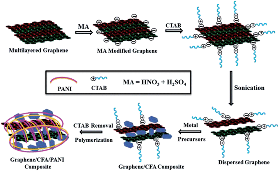 | ||
| Fig. 1 Schematic representation of the preparation of the nanocomposites. | ||
The well dispersed graphene solution means the gallery height of the layers of the graphene sheets increased, which helps the incorporation of CFA particles inside the graphene layers. After the incorporation of CFA particles, CTAB was removed by thorough washing with doubly distilled H2O, and produced the final form of the graphene/CFA composite. In the next step, the graphene/CFA/PANI composite was prepared through the polymerization of aniline.
:2. To complete the polymerization, the stirring was continued at a constant rpm for 5 h at room temperature. After the polymerization, the whole solution was filtered, washed several times with deionized water and ethanol, and then dried to get the final fine blackish powder.3. Results and discussion
3.1. XRD analysis
The structural characterization of the prepared nanocomposites was carried out by analysing their respective XRD patterns, and the plot is shown in Fig. 2. The XRD peak of pristine graphene (i.e. the characteristic 002 plane of graphene) is shown in the inset, which appears at 2θ = 25.5° (d-spacing = 3.49 Å). The graphene/CFA composite (Fig. 2a) also contains a broad peak around 2θ = 24.7° with a d-spacing of 3.6 Å. The increased d-spacing of graphene/CFA attributed to the CFA particle entered into the gallery of graphene sheets during its preparation. The other peaks of the graphene/CFA (blue star) appear due to the presence of CFA in the composite, and this can be correlated with a previous report.27 Fig. 2b shows the XRD pattern of PANI prepared through an in situ chemical oxidation polymerization technique, and it showed the semi-crystalline nature with two distinguishable broad peaks (2θ ∼ 20.7° and 25.3°) corresponding to the crystal planes 020 and 200.30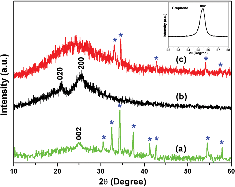 | ||
| Fig. 2 XRD pattern of graphene (inset), (a) graphene/CFA, (b) PANI and (c) graphene/CFA/PANI. | ||
Fig. 2c is the XRD plot of the graphene/CFA/PANI composite which contains a very broad peak at the initial position of the plot, and this is due to the overlapping of many peaks (peaks of PANI and graphene) present in the same region. In the case of graphene/CFA/PANI, there are few peaks and some peaks are of low intensity (with a slightly shifting position) compared to that of graphene/CFA, which means that the wrapping of PANI decreases the crystallinity, also indicating the good interfacial interaction between the components of the composites.31
3.2. X-ray photoelectron spectroscopy
To investigate the chemical composition and surface electronic state of the graphene/CFA composite, we carried out XPS analysis and this is shown in Fig. 3. The wide scan XPS spectrum of the graphene/CFA composite (Fig. 3a) confirmed the existence of all the elements (carbon, oxygen, copper, iron and aluminium) present in the graphene/CFA composite. Deconvolution of the C1s peak (Fig. 3b) of the graphene/CFA composite showed that the relative intensity of the components associated with oxygenated functional groups decreased markedly compared to those of acid modified graphene (Fig. 3c), indicating the involvement of acid modified graphene in the formation of the graphene/CFA composite.32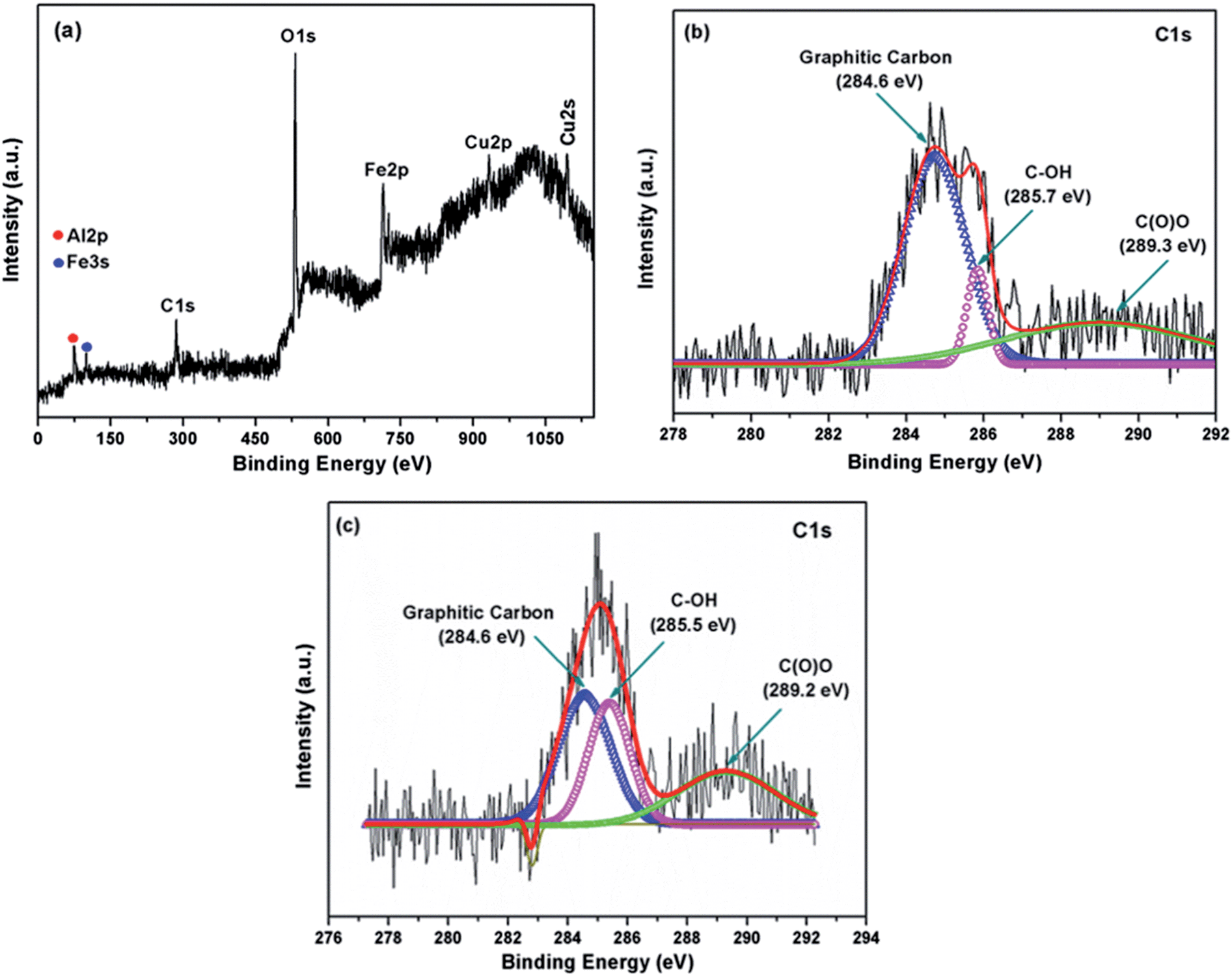 | ||
| Fig. 3 (a) Wide scan XPS spectrum of the graphene/CFA composite, (b) deconvoluted C1s XPS spectrum of graphene/CFA and (c) deconvoluted C1s XPS spectrum of acid modified graphene. | ||
Fig. 3c is the deconvoluted C1s XPS spectrum of acid modified graphene which shows three distinguishable peaks for the C–C bonds of non-oxygenated graphitic carbon (284.6 eV), C–OH bond (285.5 eV) and C(O)O bonds (289.2 eV) respectively. The peaks for the C–OH bond and C(O)O bonds are obvious as the graphene was modified by acid. The C1s spectrum of graphene/CFA also contains three peaks with slight changing in the peak position (binding energy), which is due to the interaction of graphene and CFA.33 Hence, the XPS result supports formation of the graphene/CFA composite.
3.3. Fourier transform infrared (FTIR) spectroscopy
FTIR analysis of PANI and graphene/CFA/PANI was performed to obtain their structural information, and the FTIR plot is shown in Fig. 4.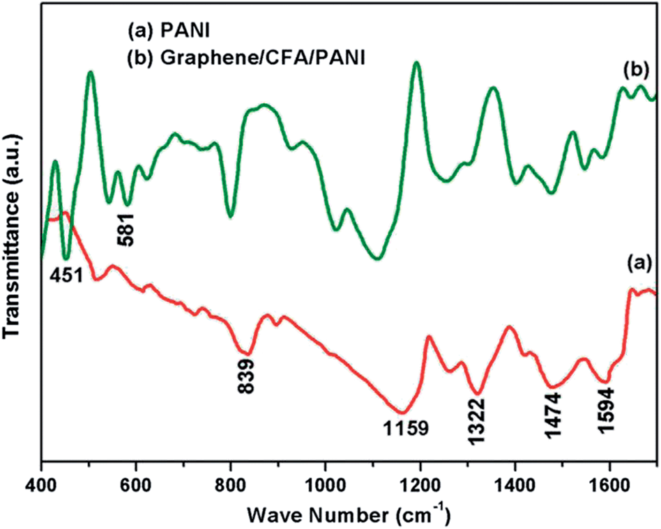 | ||
| Fig. 4 FTIR spectrum of (a) PANI and (b) graphene/CFA/PANI. | ||
The FTIR spectrum of PANI has been well reported in the literature. In this case, Fig. 4a shows the FTIR spectrum of PANI and we found that it contains all of the characteristic peaks in its spectrum. The peaks appeared at 839 cm−1, 1159 cm−1, 1322 cm−1, 1474 cm−1 and 1594 cm−1, which represent the C–H out of plane bending vibration of a 1,4-disubstituted aromatic ring, C–H bending mode of a quinoid ring, C–N and C–N+ stretching vibration mode or C–H bending mode of a benzenoid ring, C![[double bond, length as m-dash]](https://www.rsc.org/images/entities/char_e001.gif) N stretching mode of a benzenoid ring and the CC stretching mode of a quinoid ring respectively.18,24,34,35 Fig. 4b shows the FTIR spectrum of graphene/CFA/PANI which contains all the peaks that appeared for PANI. Fig. 4b also contains the peaks for CFA which appeared at 451 cm−1 and 581 cm−1. The FTIR spectrum of CFA has already been reported in a previous publication,27 which showed that the peaks of CFA are present at 439 cm−1, 550 cm−1 and 745 cm−1. Hence, the peaks of CFA are slightly shifted towards a higher wave number in the case of graphene/CFA/PANI. The peak of CFA at 745 cm−1 is not very clear in the FTIR spectrum of graphene/CFA/PANI, which may be due to the overlapping of the peaks. So, from the FTIR analysis we can assume the formation of the prepared nanocomposites.
N stretching mode of a benzenoid ring and the CC stretching mode of a quinoid ring respectively.18,24,34,35 Fig. 4b shows the FTIR spectrum of graphene/CFA/PANI which contains all the peaks that appeared for PANI. Fig. 4b also contains the peaks for CFA which appeared at 451 cm−1 and 581 cm−1. The FTIR spectrum of CFA has already been reported in a previous publication,27 which showed that the peaks of CFA are present at 439 cm−1, 550 cm−1 and 745 cm−1. Hence, the peaks of CFA are slightly shifted towards a higher wave number in the case of graphene/CFA/PANI. The peak of CFA at 745 cm−1 is not very clear in the FTIR spectrum of graphene/CFA/PANI, which may be due to the overlapping of the peaks. So, from the FTIR analysis we can assume the formation of the prepared nanocomposites.
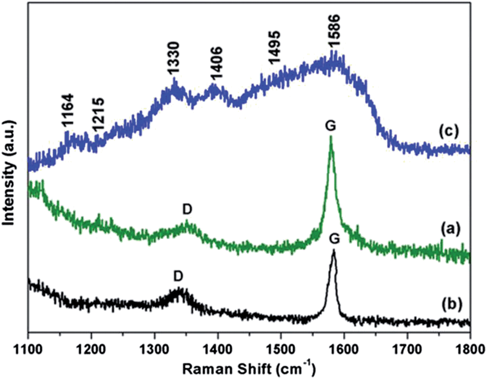
3.4. Raman spectroscopic analysis
Raman spectral measurement is an important non-destructive technique for the characterization of graphene and graphene based composites. Therefore, we used the Raman spectroscopic analysis of the prepared composites to confirm the modification of graphene with CFA, and then also with the PANI.Fig. 5 shows the representative Raman spectra of the acid modified graphene (Fig. 5a), graphene/CFA (Fig. 5b) and graphene/CFA/PANI (Fig. 5c) composites. The Raman spectra of acid modified graphene showed the characteristic D and G bands at 1350 cm−1 and 1580 cm−1 respectively. The G band is associated with E2g symmetry, and is generated due to the in-plane vibration of the sp2 carbon atoms of graphene samples, whereas the D band appears from a breathing mode of a K-point phonons of A1g symmetry.36 The G band for graphene and graphene/CFA appears as very sharp and intense, which suggests that the materials are crystalline in nature. Whereas, the crystallinity decreases (the G band becomes broad) after the modification of graphene/CFA with PANI. The broadening of the G band for graphene/CFA/PANI may be due to the coating of amorphous PANI on graphene/CFA.37 The G band of graphene/CFA slightly shifted as compared to the G band of acid modified graphene, and appears at 1584 cm−1. As in the reports of K. Singh et al., we may also suggest that the shifting of the G band indicates the charge transfer between graphene and CFA.31 The D band shifted slightly towards a lower wave number (1342 cm−1) when the acid modified graphene was further modified by CFA. This may be due to the interaction38,39 between the acid modified graphene and CFA. The Raman spectrum of graphene/CFA/PANI showed a similar pattern as that reported by S. Giri et al.34 for graphene and PANI based composites. The Raman spectrum of the graphene/CFA/PANI contains all the characteristic peaks (shown in Fig. 5c) of PANI,40,41 and also the D and G bands (the clarity of these bands is low in the spectrum as it is mixed with the peaks of PANI) coming from graphene. The Id/Ig ratio is an important parameter to measure the degree of graphitization present in a material. The Id/Ig ratio of acid modified graphene is 0.8, whereas the ratio increases to 0.9 for the graphene/CFA composite. This hike in Id/Ig ratio indicates that more defects have been introduced on graphene with the incorporation of CFA particles. Hence, the Raman spectroscopic analysis can effectively explain the formation of graphene/CFA and graphene/CFA/PANI composites.
 | ||
| Fig. 5 Raman spectra of (a) graphene, (b) graphene/CFA and (c) graphene/CFA/PANI. | ||
3.5. UV-Vis spectroscopy
The optical properties of the acid modified graphene, CFA and graphene/CFA composite are shown in ESI-S1.† The characteristic absorption peak of graphene appears at 270 nm, which is due to the π–π* transition of aromatic C–C bonds.42 The UV-Vis spectrum of graphene/CFA is different compared to the UV-Vis spectrum of its components. This result suggests that the interaction environments of all the materials with the UV-Vis radiation are different to each other. Fig. 6a shows another set of UV-Vis spectra representing PANI and the graphene/CFA/PANI composite. PANI contains three absorption peaks at 290 nm, 340 nm and 465 nm. These three peaks appear as a result of three different interactions, namely π–π*, polaron–π* and n–π*.30 However, the graphene/CFA/PANI composite contains two major peaks in its spectrum. One broad peak comes at the beginning of the spectrum, which is the mixture of many peaks coming from graphene, PANI and CFA also. The peak of PANI at 465 nm red-shifted to 576 nm in the case of graphene/CFA/PANI, which may be due to the interactions between PANI and other components of the composite.43 This red shifting could also be due to the fact that the semiconducting materials have smaller dimensions than the Bohr radius of the exciton.44 The band gap of PANI and graphene/CFA/PANI was calculated by the equation:| αhν = A(hν − Eg)n |
| αhν = A(hν − Eg)1/2. |
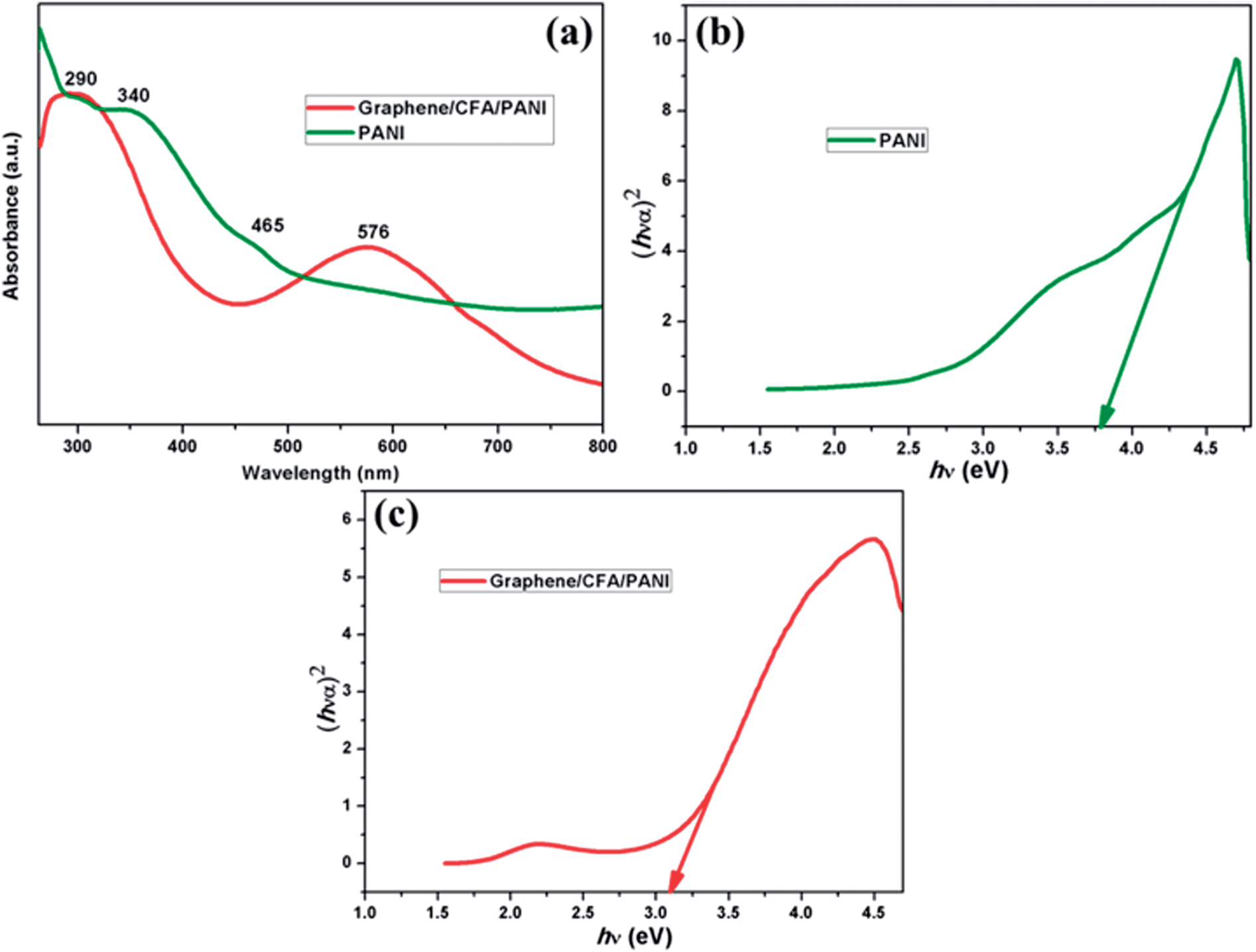 | ||
| Fig. 6 (a) UV-Vis spectrum of PANI and graphene/CFA/PANI, (b) band gap of PANI and (c) band gap of graphene/CFA/PANI. | ||
The band gaps corresponding to PANI and graphene/CFA/PANI (Fig. 6b and c) are 3.8 and 3.07 respectively. Hence, the composite formation helps to decrease the band gap or may increase the electrical conductivity.
3.6. Morphological study and energy-dispersive spectroscopy
Fig. 7a is an FESEM image of CFA particles which shows the hexagonal morphology of CFA, with some agglomerated parts formed due to the magneto dipole interactions among the magnetic CFA particles. Fig. 7b and c are the magnified FESEM images of CFA, which show the almost perfect hexagonal shaped CFA particles form together in some portions, and in some portions they remain single. Fig. 7d and e show the FESEM images of graphene/CFA and graphene/CFA/PANI nanocomposites respectively. Fig. 7d shows an FESEM image of the graphene/CFA composite. The rough surface of the image means that the CFA particles have been attached on the sheets of graphene, and confirmed the formation of the composite. We have also shown the FESEM image of the graphene/CFA/PANI composite in Fig. 7e to confirm the wrapping of PANI on the surface of the graphene/CFA composite.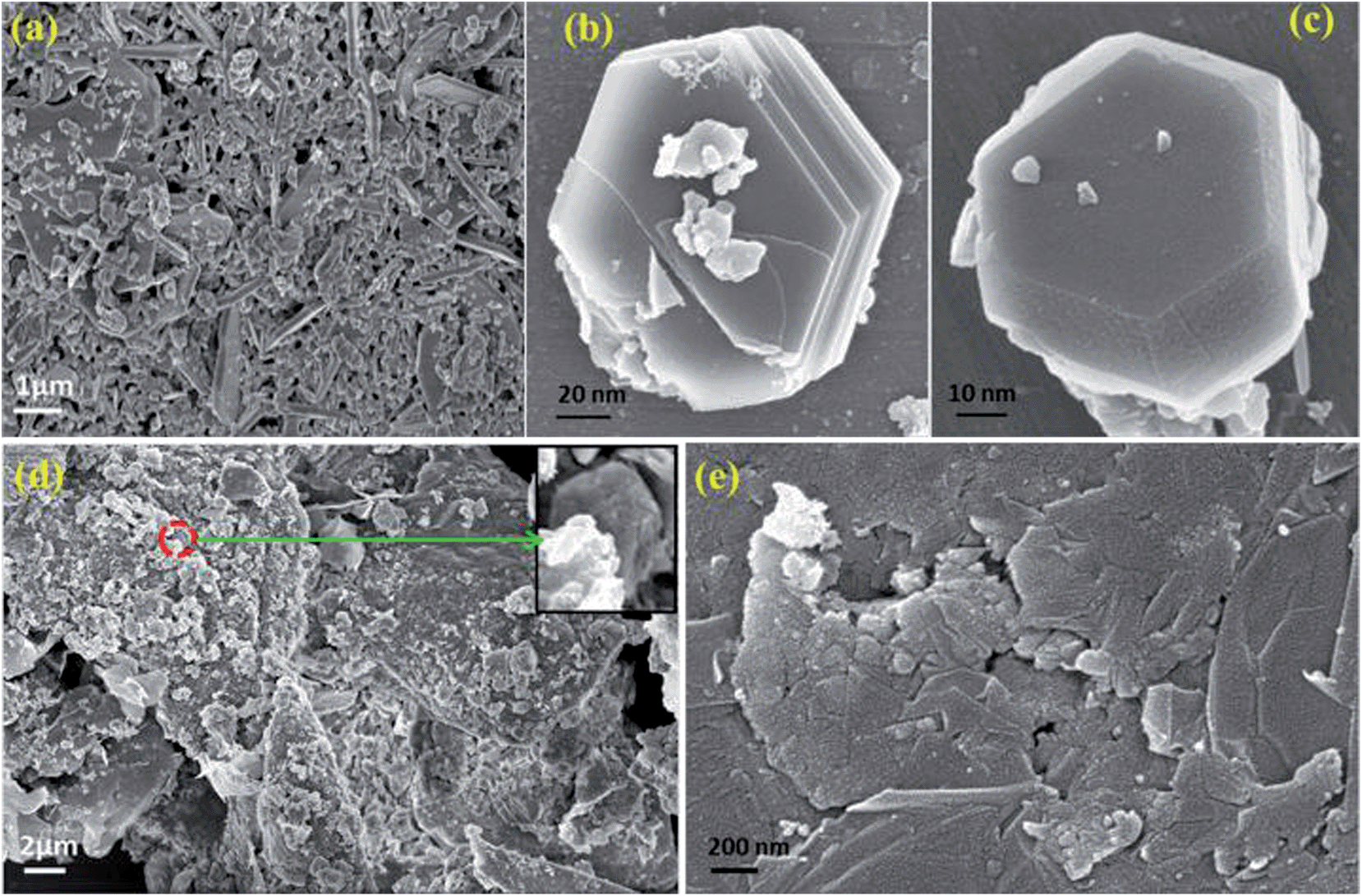 | ||
| Fig. 7 FESEM image of (a) CFA, (b & c) magnified image of CFA, (d) graphene/CFA and (e) graphene/CFA/PANI. | ||
To be sure of the formation of the materials, we produced HRTEM images of the prepared samples in Fig. 8. The hexagonal structure of CFA was again authorized by Fig. 8a and b. The inset of Fig. 8b shows the corresponding SAED (Selected Area Electron Diffraction) pattern of the CFA particles. The bright spots of the SAED image confirmed the crystalline nature of CFA. Fig. 8c shows that CFA particles were formed on the graphene surface, and some uncovered surface of graphene is also present in the material. Fig. 8d helps us to know more about the coating of PANI on the graphene/CFA composite. The presence of the graphene sheets is shown by the red coloured single headed arrows in the images.
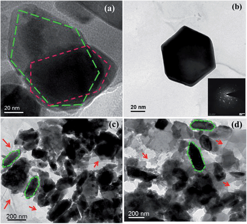 | ||
| Fig. 8 HRTEM image of (a) CFA, (b) a magnified image of CFA, SAED pattern of CFA (inset) (c) graphene/CFA and (d) graphene/CFA/PANI. | ||
The energy-dispersive spectroscopic (EDS) profile of the prepared composites (ESI-S2†) is also attached for knowledge of the elements present in the materials concerned. The graphene/CFA and graphene/CFA/PANI composite contain all of the said elements used for the preparation of these composites and the XPS results are supported.
3.7. Thermal analysis
The thermogravimetric analysis (TGA; Fig. 9) plot and corresponding derivative (DTG; ESI-S3†) plot of PANI and graphene/CFA/PANI composite are shown to display their thermal stability, which is highly desirable for high temperature applications.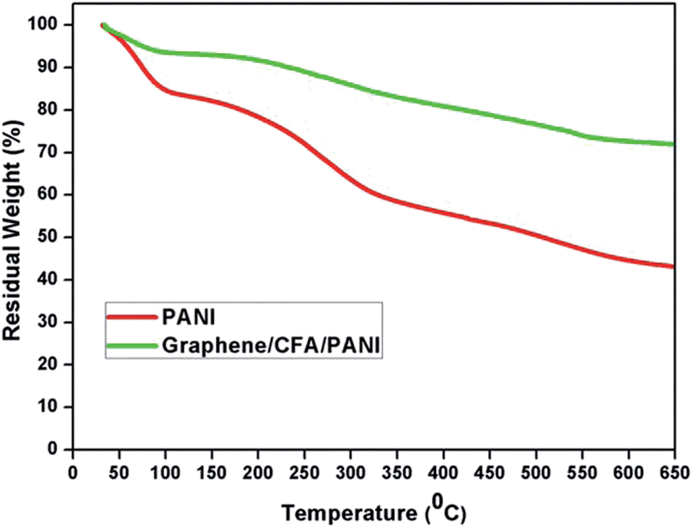 | ||
| Fig. 9 TGA plot of PANI and graphene/CFA/PANI. | ||
The initial look into the TGA plot clearly suggests that the graphene/CFA/PANI composite has greater thermal stability than that of PANI. The DTG curve of PANI contains three different degradation temperatures, minima at – (i) 63 °C, (ii) 237–286 °C and (iii) 528 °C. However, the DTG curve of the graphene/CFA/PANI composite showed the thermal degradation minima at (i) 63 °C, (ii) 260–302 °C and (iii) 542 °C. The first degradation temperature is the same for both materials, and it is due to the loss of moisture captured in the material.31 The second degradation is attributed to the exclusion of dopant material,45 and the last thermal degradation is a result of the degradation of polymer chain.46 Although the pattern of degradation is the same for both materials, the degradation temperature of the graphene/CFA/PANI composite is higher than that of PANI. The highest degradation temperature of the graphene/CFA/PANI composite suggests that the interaction between PANI and the other components of the composite helps the late degradation of the polymer chain. The total weight loss of PANI is around 62% at 800 °C, whereas it is 34% for the graphene/CFA/PANI composite. The late degradation of PANI in the graphene/CFA/PANI composite may be due to the barrier property of graphene.47 The thermal motion of the polymer becomes restricted when it enters into the gallery of graphene sheets, and hence the thermal degradation becomes slow or the thermal stability of the composite enhanced.45 Another reason for the enhancement of thermal stability of the composite is the interaction between the Fe and –NH2 groups of PANI through the coordinate bond, which is formed by the involvement of the d orbital of Fe and the –NH2 group in the back-bonding process.31
3.8. Magnetic properties
To study the magnetic properties of the as obtained nanocomposites, magnetization measurements were carried out at room temperature and the resulting hysteresis plot is shown in Fig. 10. The nature of both the sample is ferromagnetic. ESI-T1† shows a summary of the magnetic results obtained for different composites. The saturation magnetization (Ms) of graphene/CFA is lower than that of CFA, whereas, the same is higher than that of graphene/CFA/PANI. The result is obvious, because both the graphene and PANI are non-magnetic. The remanence magnetization (Mr) and coercivity (Hc) also decreased with an increase in the non-magnetic component. The coercivity of a material depends upon many factors, such as microstructure, grain shape, composition, magnetic anisotropy etc. The high coercivity value of CFA may be due to its hexagonal shape.48 Now, due to the presence of graphene and PANI the composite has a different morphology (microstructure or shape), which may result in the lowering of coercivity. The low remanence value is essential for a good microwave absorption property of the nanocomposites, because the magnetization and demagnetization process becomes easy and fast, which leads to better absorption.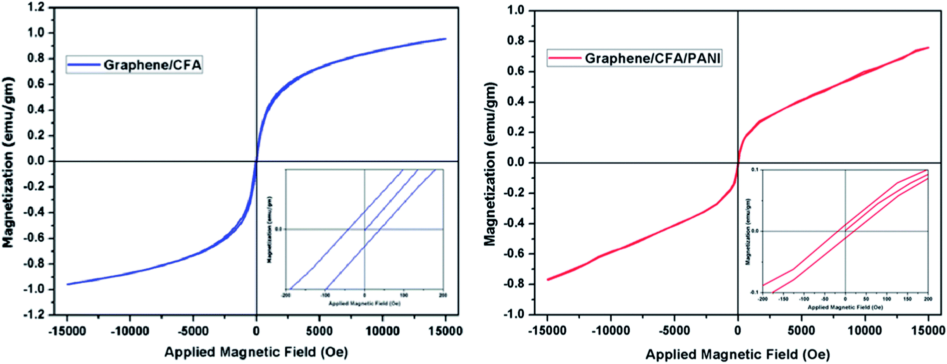 | ||
| Fig. 10 Magnetic properties of graphene/CFA and graphene/CFA/PANI. | ||
3.9. Electrical conductivity
The electrical conductivity measurements for the prepared samples are important, because both the mentioned applications (supercapacitor and microwave absorber) depend on the conductivity of a material. The DC conductivity of the samples was calculated with the help of the following equations:| resistivity (ρ, Ω cm) = πt/ln2(V/I) |
| conductivity (σ, S cm−1) = 1/ρ |
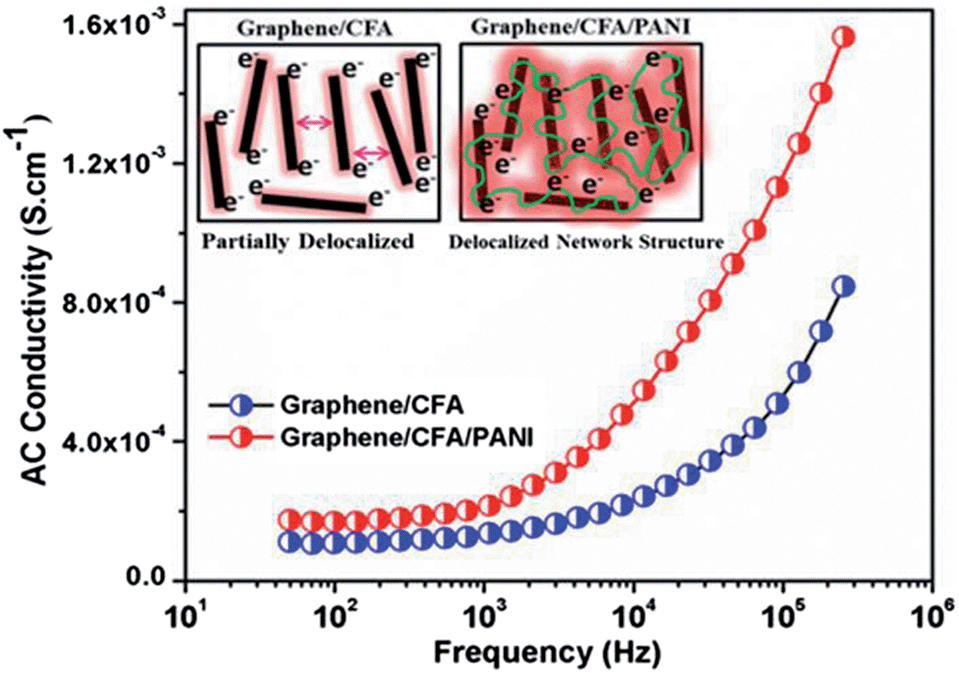 | ||
| Fig. 11 AC conductivity of graphene/CFA and graphene/CFA/PANI. | ||
The AC conductivity vs. frequency plot is shown in Fig. 11. At the low frequency region, the AC conductivity of graphene/CFA and graphene/CFA/PANI is low and remains flat. The AC conductivity increases with an increase in frequency for both the materials. The frequency at which the sudden change in AC conductivity occurs is called the critical frequency. After the critical frequency, the change in AC conductivity with frequency is very significant. At a particular frequency, the AC conductivity of graphene/CFA/PANI is higher than that of graphene/CFA. This result is consistent with the result of DC conductivity. The AC conductivity of a material at a low frequency depends on the orientational polarization of the dipoles or induced dipoles present in that material. At a low frequency, the relaxation time of the dipoles is high enough to take part in the orientational polarization along the applied electric field. Since PANI is a dielectric material, so the polarization is more for the graphene/CFA/PANI composite compared to that of the graphene/CFA composite. This is the probable reason behind the high conductivity of graphene/CFA/PANI at the low frequency region. On the contrary, the relaxation time at a high frequency is very short to the orientational polarization and so the AC conductivity does not depend on the polarization of the dipoles. At a high frequency, the AC conductivity of a composite depends on the hopping or tunnelling of the electrons. Here in the present case, the internally connected conductive network of the graphene/CFA/PANI composite increases the rate of hopping or tunnelling of electrons, which results in its better AC conductivity. Hence, both the prepared materials are conductive, but the graphene/CFA/PANI is more conductive than the graphene/CFA.
3.10. I–V characteristics
The I–V characteristics of the as prepared nanocomposites were measured within the potential range of −10 V to +10 V. The experiment was done at room temperature, and the representative I–V plot is shown in Fig. 12. Both the plots deviated from linearity which means they violate Ohm's law. This non-linear (non ohmic as V/I is not constant) increase of current with the increase in applied voltage designates that these nanocomposites are a semiconducting type of material, and they can be used for electronic device applications.50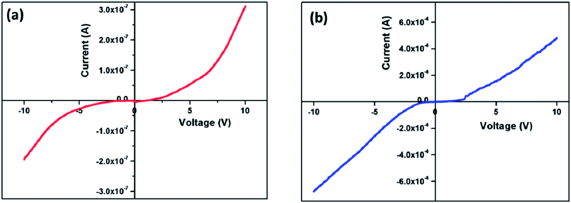 | ||
| Fig. 12 I–V plot of (a) graphene/CFA and (b) graphene/CFA/PANI. | ||
3.11. Microwave absorbing property
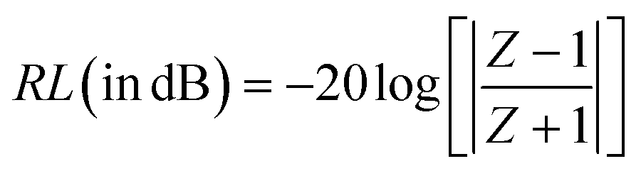
To investigate the efficiency of the prepared materials as microwave absorbers, we investigated their microwave absorbing property in the X-band region. The ability of an absorber to absorb the radiation is generally expressed in terms of reflection loss (RL). More reflection loss means more absorption. The equation used to calculate the reflection loss is: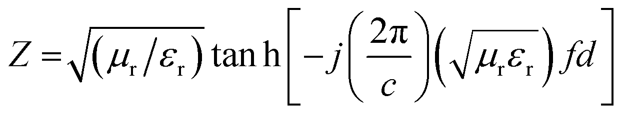
where Z is the normalized input impedance with respect to the impedance in free space and RL is in decibels (dB). εr (εr = ε′ − jε′′) and μr (μr = μ′ − jμ′′) are the relative complex permittivity and permeability of the absorber; f and c are the frequency of microwaves in free space and the velocity of light, respectively; and d is the sample thickness. The ε′ and ε′′ are known as the real and imaginary parts of the relative complex permittivity, whereas μ′ and μ′′ denote the real and imaginary part of the relative complex permeability respectively. The real and imaginary part are associated with the amount of energy stored in the material, and the amount of energy dissipated from the material respectively. The variation of RL with frequency and thickness is shown in Fig. 13.
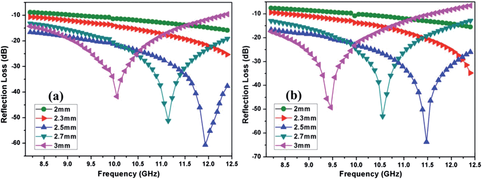 | ||
| Fig. 13 Reflection loss vs. frequency plots of (a) graphene/CFA and (b) graphene/CFA/PANI. | ||
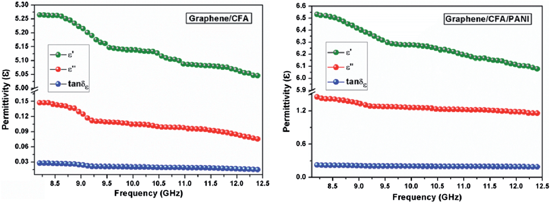
Both the prepared nanocomposites showed comparable reflection loss values (−60.7 dB for graphene/CFA and −63.6 dB for graphene/CFA/PANI) at 2.5 mm thickness. We have compared our results with some previously reported results in ESI-T2.† The value of RL for our materials is high enough to use it for many microwave absorbing applications. Fig. 13 demonstrates that the maxima of RL moves towards a lower frequency as the thickness of the absorber increases for both the materials. This type of change is beneficial, because the frequency range of absorption can be adjusted according to the requirements by altering the thickness of the material. For a potential microwave absorber the band width of absorption should be very high. In the present work, both the composites cover the whole X-band region with 90% (RL = −10 dB) absorption. Graphene/CFA covers the frequency range (with 99% absorption i.e. RL = −20 dB) of 2.8 GHz (9.6–12.4 GHz), whereas the same increases for the graphene/CFA/PANI composite (9.4–12.4). Therefore, we can conclude that both the materials are efficient broadband microwave absorbers, but graphene/CFA/PANI is superior compared to the graphene/CFA composite. The performance of a microwave absorber depends upon mainly two factors – (i) matching of impedance upon the irradiation of radiation on the surface of the material and (ii) the complementarity between the dielectric loss and magnetic loss. For the good matching of impedance, the controlling of conductivity of the absorber is an important factor. Both high and low conductivity results in bad microwave absorption. Highly conductive materials result in the skin effect, which increases the surface reflection and decreases the absorption. Graphene is highly conductive, therefore the microwave absorption of pure graphene is very low (due to the skin effect, surface reflection becomes very high). In the present case, graphene was decorated with the insulating CFA particles which reduce the conductivity (and also reduce the skin effect) of graphene to some extent, and help in the matching of impedance. Thus, the microwave absorption of the graphene/CFA composite is superb. In the case of graphene/CFA/PANI, the microwave absorption is a little bit higher than that of graphene/CFA, which indicates better impedance matching of graphene/CFA/PANI than that of the graphene/CFA composite. K. Singh et al. also observed that the addition of PANI can improve the matching of impedance.31 The enhanced microwave absorption of graphene/CFA/PANI may also be due to the charge transfer process within the components of the composites, as shown in the Raman spectra. The morphology of the prepared nanocomposites showed that the materials were composited well enough. Hence, these prepared nanocomposites may also exhibit good complementarity between the dielectric loss and magnetic loss, because the nanocomposites contain both the dielectric and magnetic materials together. The dielectric and magnetic performance of the prepared nanocomposites was investigated in terms of their relative complex permittivity and permeability. Fig. 14 shows the variation of the real, imaginary and loss tangents (tanδε = ε′′/ε′) of relative complex permittivity of the graphene/CFA and graphene/CFA/PANI nanocomposite respectively.
 | ||
| Fig. 14 Relative complex permittivity of graphene/CFA and graphene/CFA/PANI. | ||
The real and imaginary parts of the complex permittivity of the prepared nanocomposite decrease with an increase in frequency. The plot of the loss tangent initially decreases a little bit, and then it remains almost constant. The value of tanδε suggests that graphene/CFA/PANI more efficiently dissipates energy in the form of heat, as compared to the energy dissipation ability of the graphene/CFA nanocomposite. Therefore, the incorporation of PANI improved the dielectric loss of the graphene/CFA/PANI nanocomposite. The dielectric performance of an absorber depends on the extent and type of polarization present in that absorber. The different polarizations that may exist in a material can be classified as ionic, electronic, orientational, and space charge polarization. In the case of the microwave frequency range, the contribution of the orientational and space charge polarization is important. The space charge polarization is associated with the heterogeneity present at the interface between the components of the composites, and the bound charges (dipoles) present in the material is responsible for the orientational polarization. The difference in dielectric constants and electrical conductivities among the components of the composites is responsible for the generation of space charge polarization. As the prepared nanocomposites differ in their dielectric constants and electrical conductivities, so, the amount of space charge polarization and hence the permittivity values of the prepared nanocomposites are also different. The space charge polarization decreases with an increase in the frequency, which results in the decreasing trend of ε′ and ε′′ with the increase in frequency.51 The higher permittivity value of graphene/CFA/PANI may be due to the orientational or dipolar polarization that originates from the bound charges present in PANI. The representative Cole–Cole plot is shown in ESI-S4† which suggests that graphene/CFA/PANI has a higher number of semicircles than that of the graphene/CFA nanocomposites. Each semicircle corresponds to one Debye relaxation process. Therefore, we can say that both the nanocomposites showed a significant amount of the dielectric relaxation process, but it becomes high due to the presence of PANI. This difference in the dielectric relaxation process of the prepared nanocomposites causes the difference in their loss tangent values.40 Graphene/CFA/PANI has a higher loss tangent than that of the graphene/CFA nanocomposites. Higher loss tangent values of the nanocomposites favour high microwave absorption. The in situ synthesis of the nanocomposites is also beneficial to their high microwave absorption as it helps to generate more interfacial sites between the components of the nanocomposites, and therefore the polarization mechanisms occur easily.
Fig. 15 shows the plots of the real, imaginary and loss tangents (tanδμ = μ′′/μ′) of relative complex permeability of the prepared nanocomposites. The real, imaginary and loss tangent values showed a decreasing trend with increasing frequency. The graphene/CFA showed a tanδμ value a little bit higher than that of graphene/CFA/PANI, which may be due to the presence of non-magnetic PANI in graphene/CFA/PANI. The main contributor to the complex permeability of the nanocomposites is the hexaferrite, CFA. The high magneto-crystalline anisotropy of hexaferrite is essential for the strong coupling between the magnetic dipoles. At the high frequency of the applied field the induced magnetization and applied field differ from each other and magnetic loss happens.52 The domain-wall resonance and spin-rotation resonance are the two contributors to the complex permeability, but the spin-rotation resonance is the major contributor to the magnetic loss.53 The matching of dielectric loss and magnetic loss makes both the nanocomposites potential microwave absorbers. Another important absorption mechanism is that of multiple reflections, which may be due to the presence of layered graphene in the prepared nanocomposites. The multiple reflections can happen in both the nanocomposites, which help in the propagation of electromagnetic waves and enhance the absorption ability of the nanocomposites.
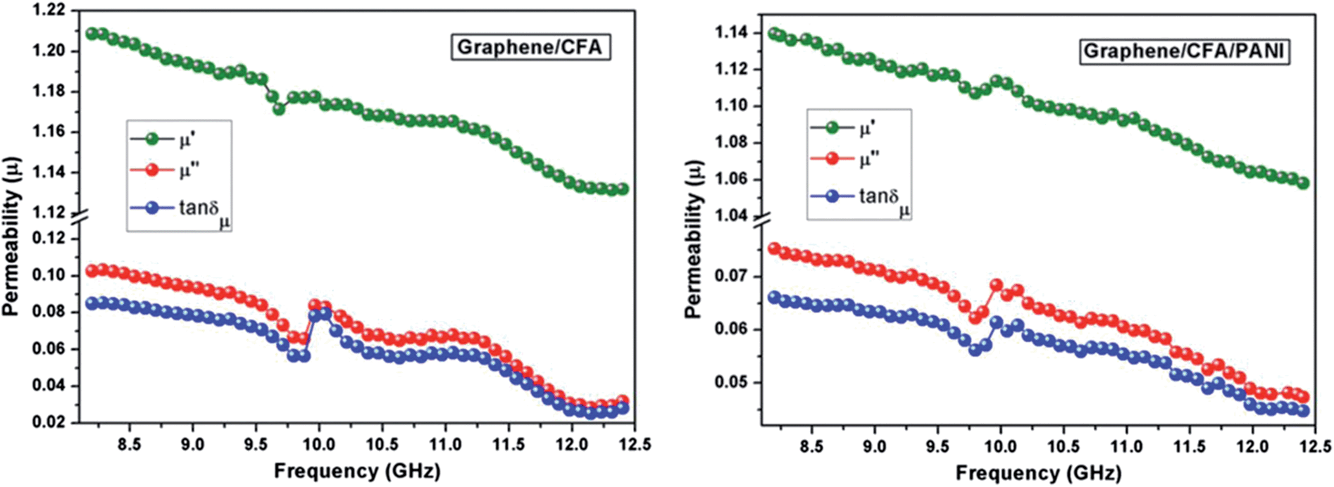 | ||
| Fig. 15 Relative complex permeability of graphene/CFA and graphene/CFA/PANI. | ||
3.12. Electrochemical characterization
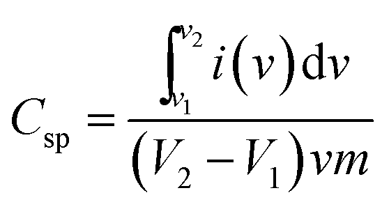
The electrochemical performance of the prepared material was investigated by means of cyclic voltammetry (CV), galvanostatic charge–discharge curves (GCD) and electrochemical impedance spectroscopy (EIS) in 1 M aqueous KCl electrolyte without any binder or carbon additive. The potential range used for the CV measurement was −0.8 V to 0.8 V. The specific capacitance of the materials was calculated by the following equation:11where, Csp is the specific capacitance obtained by CV measurements, the numerator calculates the total charge under the CV plot within the working potential range V2 and V1, ν is the scan rate and m is the mass of the composite electrode materials. In the case of three electrode cells, the capacitance values are the capacitance per electrode. The CV-plot has two regions, the negative current zone denotes the reduction in cathode and the positive current region represents the oxidation in the anode. The CV plot of graphene/CFA/PANI is shown in Fig. 16a. The shape of the plot is not perfectly rectangular, which indicates deviation from ideal supercapacitor behaviour. The plot contains some redox peaks which are due to the presence of CFA and PANI. This redox nature of the plot confirms the presence of pseudocapacitance, which contributes to the total specific capacitance of the material. We have calculated the specific capacitance of the prepared materials at different scan rates. The maximum specific capacitance for graphene/CFA/PANI is 342 F g−1 at the scan rate of 10 mV s−1. The specific capacitance value of graphene/CFA/PANI is very much higher compared to that of graphene (∼10–135 F g−1) and CFA (4 F g−1).27,54 Our material also showed a better specific capacitance than the specific capacitance of some spinel ferrite and graphene/CNT based composites which have already been reported elsewhere. Z. Wang et al. synthesized a graphene–NiFe2O4 nanocomposite and measured the specific capacitance of 153 F g−1 at a 10 mV s−1 scan rate.55 S. Giri et al. revealed the specific capacitance of 115 F g−1 at 10 mV s−1 for the MWCNT/CuFe2O4 nanocomposite.56 In one of our previous works, we reported the in situ synthesis of nanocomposites based on MWCNT and M-type hexaferrite which has the specific capacitance value of 269 F g−1.27 The inset of Fig. 16a demonstrates the specific capacitance vs. scan rate plot, which shows a decreasing trend of specific capacitance with an increase of scan rate. The decrease in specific capacitance is ∼25% when the scan rate was increased from 10 to 200 mV s−1. This decrease in specific capacitance is due to the diffusion effect of protons within the electrode material, which hampers the redox process of the inner active sites at a high scan rate.57 On the contrary, the peak current increased linearly with increasing the scan rate. This is due to the diffusion controlled doping and dedoping of the electrolyte ions and also the fast kinetics of the interfacial redox reaction.11
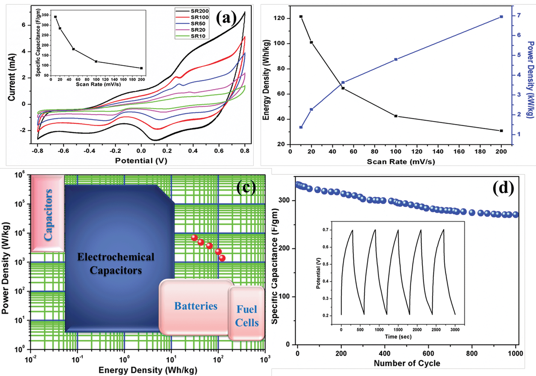 | ||
| Fig. 16 (a) CV plot, specific capacitance vs. scan rate plot (inset) (b) plot of energy density and power density with various scan rates (c) Ragone plot, (d) specific capacitance vs. the number of cycles, GCD plot (inset) of graphene/CFA/PANI. | ||
The performance of a good hybrid supercapacitor cannot be judged only by the value of specific capacitance. A good supercapacitor should have the qualities, such as excellent energy and power density, high cyclic stability, good reversibility etc. Therefore, we have also paid our attention to determine the energy and power density by using the equations:
| energy density (E) = 1/2(CV2) |
| power density (P) = (E/t) |
(1) The total capacitance of a material depends on the summation of double layer capacitance (non-Faradaic process) and pseudocapacitance (Faradaic process). Here, in our case, graphene is responsible for generating the double layer capacitance, and the pseudocapacitance is resultant from the CFA and PANI. Hence, the overall capacitance of the composite increases, as compared to that of its components.
(2) The high surface area and high porosity of graphene facilitates the ion diffusion process of the electrolyte ions and thus the double layer capacitance increases. Moreover, the good electrical conductivity of graphene may speed up the charge transfer process among CFA, PANI and graphene, which further helps to improve the electrochemical properties of the composite.
To further investigate the feasibility of the electrode material, a galvanostatic charge–discharge (GCD) test was performed at a current density of 1 A g−1. The voltage range was maintained from 0.2–0.7 V during the GCD test, as shown in the inset of Fig. 16d. The specific capacitance from the GCD plot can be calculated by the equation:
| Specific capacitance = CGCD = i × Δt/(Δv × m) |
| η = [discharging time (tD)/charging time (tC)] × 100%. |
The Coulombic efficiency (calculated with respect to the second GCD cycle) of graphene/CFA/PANI is 104%, which is good for potential supercapacitor applications. The GCD test was continued up to 1000 cycles. To know the cyclic stability of graphene/CFA/PANI, we have plotted the specific capacitance vs. the number of cycles and it is shown in Fig. 16d. After 800 cycles, the specific capacitance remains stable and the retention of specific capacitance is ∼81.2%, which is also excellent for supercapacitor applications.
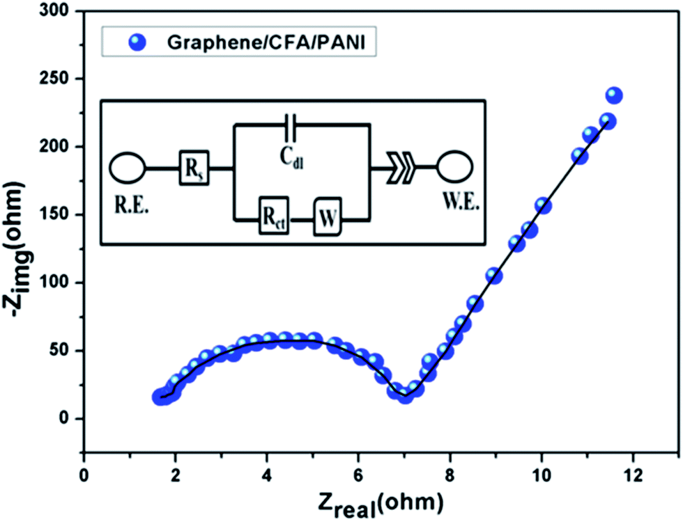
In addition, we have performed the EIS study and the corresponding Nyquist plot (at 0 volt) of graphene/CFA/PANI is shown in Fig. 17 along with the fitted curve. The equivalent electrical circuit used for fitting is shown in the inset of Fig. 17.
 | ||
| Fig. 17 Nyquist plot of graphene/CFA/PANI. | ||
A Nyquist plot is the plot of the imaginary vs. real components of the impedance study, and gives the frequency response of the electrode–electrolyte system.34 The higher frequency region is associated with the electrolyte properties, and the mid frequency region corresponds to the electrode–electrolyte interface processes. The solution resistance (Rs) and charge transfer resistance (Rct) are the intercept of the curve at high frequency and mid frequency with the real axis respectively. An impedance response of a 45° straight line is known as the Warburg resistance (W) which signifies the mass transfer parameters of the electrochemical doping process. The Nyquist plot of graphene/CFA/PANI contains one semicircle at the high frequency region, and one straight line at the low frequency region. The diameter of the semicircle can be attributed to the value of Rct. The higher the diameter of the semicircle indicates a higher value of Rct. The Rs and Rct of graphene/CFA/PANI are 1.6 Ω and 7.1 Ω respectively. The low Rct value may result due to the high conductivity of graphene/CFA/PANI. The straight line at the low frequency region of the Nyquist plot is significant with the diffusion of electrolyte ions within the electrode material.11 For an ideal capacitor, this straight line should be parallel to the imaginary axis of the Nyquist plot. Graphene/CFA/PANI deviates from the behaviour of an ideal capacitor as the straight line is not parallel to the imaginary impedance axis. In real-world systems, ideal capacitors do not exist. The non-ideal behaviour of a capacitor can be demonstrated by constant phase element (CPE), which is recognised by a depressed semicircle in the Nyquist plot. The increase in CPE means an increase in the ideal character of a capacitor. The CPE of an electrode can be the result of inhomogeneous distribution of reactive sites on an electrode or the rough surface of the electrode.58 CPE can be defined by the equation:
| ZCPE = [Q0(jω)n]−1 |
Z vs. log f plot. The value of n covers a range from 0 to 1. For an ideal capacitor n = 1, for a resistor n = 0 and n = 0.5 indicates the Warburg behaviour. The value of n for graphene/CFA/PANI is 0.79. Hence, our material can act as a good capacitor.
4. Conclusion
The present work demonstrates the successful synthesis of thermally stable multifunctional nanocomposites based on graphene, M-type hexaferrite (CFA) and PANI with remarkable microwave absorption and electrochemical properties. The synthetic procedure is simple and feasible. The formation of nanocomposites and their structural characteristics were discussed thoroughly with their impact on the two different fields of applications i.e. microwave absorbing and energy storage device applications. The highest reflection loss of graphene/CFA/PANI is −63.6 dB and the same for graphene/CFA is −60.6 dB at the thickness of 2.5 mm with a broad absorption range. This excellent microwave absorption of the prepared nanocomposites is due to the summation of good impedance matching characteristics, good complementarity of dielectric loss (due to graphene and PANI) and magnetic loss (due to CFA), good electrical conductivity, special structural characteristics etc. The prepared nanocomposites can also be used as efficient electrode materials for supercapacitor applications. The capacitance properties of the nanocomposites are the result of both double layer capacitance and pseudocapacitance. The in situ technique is important to improve the interfacial interactions between the components of the nanocomposites, which leads to the improved electrochemical and microwave absorption properties. Hence, these nanocomposites can be effectively synthesized as per the demands for the applications of potential microwave absorbers and also for the energy storage device applications as well.Acknowledgements
The authors are thankful to IIT Kharagpur, India for providing the instrumental facilities. Authors are also thankful to Council of Scientific and Industrial Research (CSIR), New Delhi, India; UGC, New Delhi, India and Defence Research & Development Organization (DRDO), India for providing the fellowship.References
- H. P. Cong, X. C. Ren, P. Wang and S. H. Yu, ACS Nano, 2012, 6, 2693–2703 CrossRef CAS PubMed.
- Z. Niu, J. Chen, H. H. Hng, J. Ma and X. Chen, Adv. Mater., 2012, 24, 4144–4150 CrossRef CAS PubMed.
- Y. Zhao, C. Hu, Y. Hu, H. Cheng, G. Shi and L. Qu, Angew. Chem., 2012, 124, 11533–11537 CrossRef PubMed.
- S. Liu, F. Lu, Y. Liu, L-P. Jiang and J-J. Zhu, J. Nanopart. Res., 2013, 15, 1331 CrossRef.
- J. Cao, W. Fu, H. Yang, Q. Yu, Y. Zhang, S. Liu, P. Sun, X. Zhou, Y. Leng, S. Wang, B. Liu and G. Zou, J. Phys. Chem. B, 2009, 113, 4642–4647 CrossRef CAS PubMed.
- S. Motojima, S. Hoshiya and Y. Hishikawa, Carbon, 2003, 41, 2658–2660 CrossRef CAS.
- J. Zhou, J. He, G. Li, T. Wang, D. Sun, X. Ding, J. Zhao and S. Wu, J. Phys. Chem. C, 2010, 114, 7611–7617 CAS.
- G. Li, T. Xie, S. Yang, J. Jin and J. Jiang, J. Phys. Chem. C, 2012, 116, 9196–9201 CAS.
- C. Liu, F. Li, L. P. Ma and H. M. Cheng, Adv. Mater., 2010, 22, E28–E62 CrossRef CAS PubMed.
- V. Aravindan, M. V. Reddy, S. Madhavi, S. G. Mhaisalkar, G. V. Subba Rao and B. V. R. Chowdari, J. Power Sources, 2011, 196, 8850–8854 CrossRef CAS PubMed.
- D. Ghosh, S. Giri and C. K. Das, Nanoscale, 2013, 5, 10428–10437 RSC.
- Z. Fan, J. Chen, K. Cui, F. Sun, Y. Xu and Y. Kuang, Electrochim. Acta, 2007, 52, 2959–2965 CrossRef CAS PubMed.
- A. A. Balandin, S. Ghosh, W. Z. Bao, I. Calizo, D. Teweldebrhan, F. Miao and C. N. Lau, Nano Lett., 2008, 8, 902 CrossRef CAS PubMed.
- Y. B. Zhang, J. P. Small, M. E. S. Amori and P. Kim, Phys. Rev. Lett., 2005, 94, 176803 CrossRef.
- H. B. Zhang, W. G. Zheng, Q. Yan, Y. Yang, J. W. Wang, Z. H. Lu, G. Y. Ji and Z. Z. Yu, Polymer, 2010, 51, 1191 CrossRef CAS PubMed.
- L. Sun, C. Tian, M. Li, X. Meng, L. Wang, R. Wang, J. Yin and H. Fu, J. Mater. Chem. A, 2013, 1, 6462 CAS.
- X. Xia, W. Lei, Q. Hao, W. Wang and X. Wang, Electrochim. Acta, 2013, 99, 253–261 CrossRef CAS PubMed.
- P. Bhattacharya and C. K. Das, J. Mater. Sci.: Mater. Electron., 2013, 24, 1927–1936 CrossRef CAS PubMed.
- C. Doroftei, E. Rezlescu, P. D. Popa and N. Rezlescu, J. Optoelectron. Adv. Mater., 2006, 8, 1023–1027 CAS.
- K. Chen, L. Li, G. Tong, R. Qiao, B. Hao and X. Liang, Synth. Met., 2011, 161, 2192–2198 CrossRef CAS PubMed.
- P. Xu, X. Han, C. Wang, H. Zhao, J. Wang, X. Wang and B. Zhang, J. Phys. Chem. B, 2008, 112, 2775–2781 CrossRef CAS PubMed.
- A. Ohlan, K. Singh, A. Chandra and S. K. Dhawan, ACS Appl. Mater. Interfaces, 2010, 2, 927–933 CAS.
- H. Zhang, A. Xie, C. Wang, H. Wang, Y. Shen and X. Tian, ChemPhysChem, 2014, 15, 366–373 CrossRef CAS PubMed.
- P. Bhattacharya, S. Dhibar and C. K. Das, Polym.-Plast. Technol. Eng., 2013, 52, 1–8 CrossRef.
- Y. Jia, Z. M. Jiang, X. L. Gong and Z. Zhang, eXPRESS Polym. Lett., 2012, 6, 750–758 CrossRef CAS.
- P. Bhattacharya, C. K. Das and S. S. Kalra, J. Mater. Sci. Res., 2012, 1, 126–132 CAS.
- P. Bhattacharya and C. K. Das, Ind. Eng. Chem. Res., 2013, 52, 9594–9606 CrossRef CAS.
- J. Rausch, R. C. Zhuang and E. Mader, Composites, Part A, 2010, 41, 1038–1046 CrossRef PubMed.
- D. Wu, F. Zhang, H. Liang and X. Feng, Chem. Soc. Rev., 2012, 41, 6160–6177 RSC.
- J. Yan, T. Wei, Z. Fan, W. Qian, M. Zhang, X. Shen and F. Wei, J. Power Sources, 2010, 195, 3041–3045 CrossRef CAS PubMed.
- K. Singh, A. Ohlan, V. H. Pham, R. Balasubramaniyan, S. Varshney, J. Jang, S. H. Hur, W. M. Choi, M. Kumar, S. K. Dhawan, B. S. Kong and J. S. Chung, Nanoscale, 2013, 5, 2411 RSC.
- X. An, J. C. Yu, Y. Wang, Y. Hu, X. Yu and G. Zhang, J. Mater. Chem., 2012, 22, 8525 RSC.
- A. Prakash, S. Chandra and D. Bahadur, Carbon, 2012, 50, 4209–4219 CrossRef CAS PubMed.
- S. Giri, D. Ghosh and C. K. Das, J. Electroanal. Chem., 2013, 697, 32–45 CrossRef CAS PubMed.
- D. Yuping, W. Guangli, L. Xiaogang, J. Zhijiang, L. Shunhua and L. Weiping, Solid State Sci., 2010, 12, 1374–1381 CrossRef PubMed.
- S. K. Singhal, M. Lal, Lata, S. R. Kabi and R. B. Mathur, Adv. Nat. Sci.: Nanosci. Nanotechnol., 2012, 3, 045011 CrossRef CAS.
- T. Tsuji, K. Onuma, A. Yamamoto, M. Iijima and K. Shiba, Proc. Natl. Acad. Sci. U. S. A., 2008, 105, 16866–16870 CrossRef CAS PubMed.
- Y. Wang, R. Shi, J. Lin and Y. Zhu, Appl. Catal., B, 2010, 100, 179–183 CrossRef CAS PubMed.
- Y. Liu, R. Deng, Z. Wang and H. Liu, J. Mater. Chem., 2012, 22, 13619 RSC.
- H. Yu, T. Wang, B. Wen, M. Lu, Z. Xu, C. Zhu, Y. Chen, X. Xue, C. Sun and M. Cao, J. Mater. Chem., 2012, 22, 21679 RSC.
- E. C. Gomes and M. A. S. Oliveira, Am. J. Polym. Sci., 2012, 2, 5–13 CrossRef PubMed.
- W. Liu, Y. Zhang, S. Ge, X. Song, J. Huang, M. Yan and J. Yu, Anal. Chim. Acta, 2013, 770, 132–139 CrossRef CAS PubMed.
- C. C. Yang, Y. J. Gung, C. C. Shih, W. C. Hung and K. H. Wu, J. Magn. Magn. Mater., 2011, 323, 933–938 CrossRef CAS PubMed.
- D. S. Dhawale, R. R. Salunkhe, V. S. Jamadade, T. P. Gujar and C. D. Lokhande, Appl. Surf. Sci., 2009, 255, 8213–8216 CrossRef CAS PubMed.
- D. Lee and K. Char, Polym. Degrad. Stab., 2002, 75, 555–560 CrossRef CAS.
- Y. Wei and K. F. Hsueh, J. Polym. Sci., Part A: Polym. Chem., 1989, 27, 4351 CrossRef CAS PubMed.
- B. Yu, X. Wang, W. Xing, H. Yang, X. Wang, L. Song, Y. Hu and S. Lo, Chem. Eng. J., 2013, 228, 318–326 CrossRef CAS PubMed.
- Y. X. Gong, L. Zhen, J. T. Jiang, C. Y. Xu, W. S. Wang and W. Z. Shao, CrystEngComm, 2011, 13, 6839 RSC.
- S. Maiti and B. B. Khatua, RSC Adv., 2013, 3, 12874–12885 RSC.
- C. Bora and S. K. Dolui, Polymer, 2012, 53, 923 CrossRef CAS PubMed.
- D. K. M. Al-Nasrawy, IEE Proceedings, Part G: Circuits, Devices and Systems, 2011, 9, 409 Search PubMed.
- K. Ishino and Y. Narumiya, Cer. Bull., 1987, 66, 1469 CAS.
- H. J. Kwon, J. Y. Shin and J. H. Oh, J. Appl. Phys., 1994, 75, 6109–6111 CrossRef CAS PubMed.
- S. Sahoo, G. Karthikeyan, G. C. Nayak and C. K. Das, Synth. Met., 2011, 161, 1713–1719 CrossRef CAS PubMed.
- Z. Wang, X. Zhang, Y. Li, Z. Liu and Z. Hao, J. Mater. Chem. A, 2013, 1, 6393 CAS.
- S. Giri, D. Ghosh, A. P. Kharitonov and C. K. Das, Funct. Mater. Lett., 2012, 5, 1250046–1250051 CrossRef.
- G. R. Li, Z. P. Feng, J. H. Zhong, Z. L. Wang and Y. X. Tong, Macromolecules, 2010, 43, 2178–2183 CrossRef CAS.
- D. Ghosh, S. Giri, A. Mandal and C. K. Das, Appl. Surf. Sci., 2013, 276, 120–128 CrossRef CAS PubMed.
Footnote |
| † Electronic supplementary information (ESI) available: Details of the materials, characterization techniques, supporting figures and tables. See DOI: 10.1039/c4ra00448e |
| This journal is © The Royal Society of Chemistry 2014 |