Thermally-derived liquid phase involving multiphase Cu(In,Ga)Se2 nanoparticles for solution-processed inorganic photovoltaic devices†
Yeong-Hui Seoa,
Yejin Joa,
Youngmin Choia,
KyungHoon Yoonb,
Beyong-Hwan Ryua,
SeJin Ahn*b and
Sunho Jeong*a
aAdvanced Materials Division, Korea Research Institute of Chemical Technology (KRICT), 141 Gajeongro, Yuseong, Daejeon 305-600, Korea. E-mail: sjeong@krict.re.kr
bSolar Energy Department, Korea Institute of Energy Research (KIER), 71-2 Jang-dong, Yuseong-gu, Daejeon 305-343, Korea. E-mail: swisstel@kier.re.kr
First published on 8th April 2014
Abstract
In the past decade, wet chemical strategies for solution-based Cu(In,Ga)Se2 (CI(G)Se) photovoltaic devices have gained a tremendous amount of attention in solar-cell research fields. In particular, nanoparticles allowing for liquid-phase densification have been recognized as viable candidates for advancements in photovoltaic devices. In this study, multiphase CIGSe nanoparticles are synthesized by the microwave-assisted solvothermal method, in which the chemically incorporated CuSe2 and Se phases form liquid phases for inducing vigorous reactions at elevated temperatures. The morphological/crystalline structural properties of multiphase nanoparticles are analyzed, in conjunction with the temperature dependent evolution in multiphase nanoparticle-incorporating functional layers. Furthermore, we examine physical parameters including the cell performance, shunt conductance, and series resistance for multiphase CIGSe nanoparticle-derived solar cells, from which the cell performance-limiting factors are discussed.
1. Introduction
Various chalcogen-based materials have received much attention as a basic building block for light-absorbing layers applicable to thin-film solar cells. Among them, Cu(In,Ga)Se2 (CI(G)Se) and CuZnSnS4 (CZTS) have been exploited in recent decades as multicomponent materials for high-performance photovoltaic devices.1,2 In particular, the CI(G)Se-based absorber layers have been widely researched, showing high conversion efficiency levels reaching 20% as well as excellent environmental stability.3 To date, CI(G)Se-based absorber layers for high-performance photovoltaic devices have been fabricated through well-established vacuum-based deposition techniques, three-stage co-evaporation methods and two-step sputtering methods.3,4 However, in order to realize low-cost, large-area solar cells, inexpensive, non-toxic, chemical route-based, solution-processable methodologies are required with the generation of highly efficient photovoltaic devices.Recently, two distinct chemical approaches have been suggested for the realization of solution-processed CI(G)Se absorber layers. The first is based on the incorporation of metal salts as precursors for generating device-quality absorber layers.5,6 The prerequisite in this approach is merely the simple formulation of an ink or a paste containing the Cu, In, and Ga cations, from commercially available compounds, as well as organic additives to adjust the rheological properties. However, this method is associated with several processing drawbacks: a multiple coating process for a desirable thickness around 1–2 μm and an additional/sequential annealing step for eliminating the inherently-incorporated impurities (from metal salts and organic additives). The second approach is a classical, nanoparticle-based methodology that has been, in general, exploited in various wet-chemistry approaches.7–9 However, in this methodology, the most crucial requisite for the formation of the CI(G)Se absorber layer is the capability to lead to microstructural densification, unlike the other application-oriented nanoparticles. Porous particulate films, which do not undergo a densification reaction, suffer from a high leakage current, with extremely low conversion efficiencies.7,10 The conventional densification reaction is derived through an atomic rearrangement between neighboring particles at elevated temperatures close to the melting point.11 However, the melting point of the CI(G)Se phase is unfortunately much higher than the softening temperature of the glass substrate. As alternatives, the chemical densification reaction through the replacement of S with Se (ref. 12) and the liquid-phase densification through the mass transport inside a liquid-like phase,7,8 have been suggested, showing the high conversion efficiency above 8%. In particular, the liquid-phase densification process has the advantages: the versatility to be applied to other material system and the full-understanding on basic mechanisms for the case of vacuum-deposited corresponding layers. In this characteristic approach, the incorporation of low melting-point phases, which can melt below 530 °C, is of paramount importance for inducing the vigorous densification reaction.7 However, to date, the formation of device-quality, particulate CI(G)Se absorber layer through a liquid-phase densification has been rarely achieved due to the lack of in-depth study in incorporating chemically the low-melting point phase in CI(G)Se-based nanoparticle systems. In particular, the Ga-added CuInSe2 phase has not been demonstrated due to the challenges associated with the realization of Ga-added multicomponent nanoparticle systems,8 even given the fundamental probability of improvements in the performance levels of devices.
In this study, we demonstrate a chemical pathway based on multiphase, stoichiometric CIGSe nanoparticles that can undergo a liquid-phase densification reaction. A microwave-assisted solvothermal method, introduced earlier in our previous publications,7,8 is adopted to enable controllability of the compositional ratio of Cu/(In + Ga) and Ga/(In + Ga), one of the most important variables in CI(G)Se solar cells, and to control the crystalline structural evolution of the low-melting-point phases. The temperature-dependent microstructural evolution at elevated temperatures is also studied, and factors which should be taken into consideration when developing device-quality absorber layers are suggested in conjunction with an investigation of the performance levels of devices.
2. Experimental section
2.1. Raw materials
All reagents for metal sources, copper(II) acetate monohydrate (Cu(CO2CH3)2·H2O, 98+%), indium(III) acetate (In(C2H3O2)3, 99.99%), gallium(III) acetylacetonate ([CH3COCH![[double bond, length as m-dash]](https://www.rsc.org/images/entities/char_e001.gif) C(O–)CH3]3Ga), and selenium powder (Se, 99.99%) were purchased from Aldrich and used as received without further purification. Polyethylene glycol 400 (PEG 400, Junsei, H[OCH2CH2]nOH, Mw = 400, extra pure) was used as a solvent. Ethyl alcohol (EtOH, Burdick & Jackson, CH3CH2OH, ACS/HPLC certified grade) was used for the centrifugation of the synthesized multiphase CIGSe nanoparticles and for the preparation of multiphase CIGSe nanoparticle ink. Ethylene glycol (EG, Junsei, HOCH2CH2OH, guaranteed reagent) was used as a solvent for the ink preparation, and polyvinylpyrrolidone (PVP, Aldrich, (C6H9NO)n, Mw = 55
C(O–)CH3]3Ga), and selenium powder (Se, 99.99%) were purchased from Aldrich and used as received without further purification. Polyethylene glycol 400 (PEG 400, Junsei, H[OCH2CH2]nOH, Mw = 400, extra pure) was used as a solvent. Ethyl alcohol (EtOH, Burdick & Jackson, CH3CH2OH, ACS/HPLC certified grade) was used for the centrifugation of the synthesized multiphase CIGSe nanoparticles and for the preparation of multiphase CIGSe nanoparticle ink. Ethylene glycol (EG, Junsei, HOCH2CH2OH, guaranteed reagent) was used as a solvent for the ink preparation, and polyvinylpyrrolidone (PVP, Aldrich, (C6H9NO)n, Mw = 55![[thin space (1/6-em)]](https://www.rsc.org/images/entities/char_2009.gif) 000) was incorporated as an organic additive.
000) was incorporated as an organic additive.
2.2. Synthesis of multiphase CIGSe nanoparticles through a microwave-assisted solvothermal method
0.81 g (4.0 mmol) of copper(II) acetate monohydrate, 1.02 g (3.5 mmol) of indium(III) acetate, 0.55 g (1.5 mmol) of gallium(III) acetylacetonate, and 0.79 g (10.0 mmol) of selenium powder were dissolved in 20 g of PEG 400. In our previous report based on microwave (MW) irradiation, the crystalline phases were predominantly determined by the chemical role of polyol solvents.7 Multiphase chalcopyrite nanoparticles were formed by a strong steric hindrance against the chemical reaction ability of metal cations with the use of PEG 400, which has a long hydrocarbon chain between two hydroxyl groups.7 For the MW-assisted synthesis of multiphase CIGSe nanoparticles, the precursor solution was transferred to a Teflon-lined vessel after stirring for 1 h at room temperature. The precursor solution was heated under MW irradiation at 280 °C for 25 min. Upon the completion of the synthesis reaction, the reaction solution was cooled to room temperature and the nanoparticles were separated by centrifugation, collected, and washed three times with EtOH. Then, the resulting nanoparticles were dried under vacuum overnight at 40 °C, resulting in a black powder.2.3. Ink preparation and film formation
To prepare the ink, 2.5 g of the multiphase CIGSe nanoparticles were added to a solvent with 5 g of EG. The multiphase CIGSe solution was initially mixed by planetary ball milling to break agglomerated nanoparticles. Then, 5 g of EtOH and PVP as an organic additive to form a crack-free layer were added into the initially dispersed multiphase CIGSe precursor. Next, the prepared ink was dispersed by ball milling and was deposited on molybdenum (Mo)-coated soda lime glass substrate. Mo was deposited as a back contact layer by sputtering with a thickness of 1 μm. The solution-processed thin film was dried at 80 °C in a vacuum oven. Selenization was carried out in a vacuum evaporator equipped with Knudsen-type effusion cell. The chamber was evacuated to base pressure of 5 × 10⁻⁶ torr, and elemental Se was evaporated. The flux of the Se vapor was adjusted according to the effusion cell temperature and the Se was effused at 220 °C. The samples were selenized at 300, 400, and 550 °C for 3 h on a hot plate located in a chamber. A shutter connected to the hot plate was opened at 200 °C during each of the three trials. The ramping rate of the hot plate was 5 °C min−1 and 60 °C min−1 before and after the shutter was opened, respectively.2.4. Solar cell fabrication
The coated absorber layer selenized at 550 °C was integrated into a photovoltaic device following standard procedures, including the chemical bath deposition of CdS (60 nm) buffer layer, the RF sputtering of i-ZnO (50 nm) and Al-doped n-ZnO (500 nm) window layer, and the thermal evaporation of the patterned Al grid as a current collector. An antireflection layer was not deposited onto the devices tested in this study. Finally, the devices were mechanically scribed into individual cells with an active area of 0.44 cm2.2.5. Measurements
The morphological properties, crystalline phase, and composition of the multiphase CIGSe nanoparticles were analyzed using a field emission scanning electron microscope (FE-SEM, JSM-6700F, JEOL), X-ray diffraction (XRD, D/Max 2200V/PC, Rigaku), and inductively coupled plasma mass spectrometry (ICPMS, Thermo Scientific iCAP 6500), respectively. Scanning transmission electron microscopy (STEM) image and the TEM-energy dispersive X-ray spectroscopy (EDS) compositional profile for multiphase CIGSe nanoparticles were analyzed using a field emission transmission electron microscope (FE-TEM, Tecnai F20, Philips). The composition and phase transformation of the multiphase CIGSe films after the selenization process were analyzed by EDS (Quantax 200, Bruker) and XRD measurements, respectively. Surface images and the morphological changes in the multiphase CIGSe films after selenization were analyzed by an optical microscope (OM, iCamscope, Sometech Vision) and FE-SEM, respectively. A depth compositional profile of the selenized film at 550 °C was obtained by auger electron spectroscopy (AES, SAM 4300, Perkin Elmer). The conversion efficiency of the device was characterized using a class AAA solar simulator (WXS-155S-L2, WACOM, Japan).3. Result and discussion
The microwave-assisted solvothermal method allows for the formation of well-crystallized nanostructured particles via the instant supply of thermal energy. In particular, as reported previously, the phase evolution in chalcopyrite-based multiphase nanoparticles can be kinetically tailored depending on the nature of the solvent molecules and the synthetic conditions (i.e., the reaction temperature and time).7 As shown in Fig. 1a, multiphase, stoichiometric CIGSe nanoparticles were obtained when the reactant mixture containing a PEG 400, as a microwave-absorbing solvent and a reaction medium, was heated up to 280 °C for 25 min. The main phase of CuIn0.7Ga0.3Se2 was observed with the presence of other secondary phases, CuInSe2, CuSe2, GaSe, and Se. A part of Cu, In, Ga, and Se not involved in the formation of the CuIn0.7Ga0.3Se2 main phase was transformed into various secondary phases; among them, the CuSe2 and Se phase could take part in triggering of liquid-phase densification below 550 °C. The melting points of CuSe2 and Se are 523 °C and 221 °C, respectively. The measured particle size was ∼60 nm (Fig. S1a†). Unlike general nanoparticle-derived functional layers,13 the morphological properties of CI(G)Se nanoparticles are not of crucial importance, as the on-set temperature for a solid-state densification reaction does not decrease dramatically depending on the diameter of CI(G)Se-based nanoparticles.10 Rather, exploiting a chemical methodology for incorporating the melting phases is a more critical prerequisite of a vigorous densification reaction. The formation of multiphase CIGSe-based nanoparticles was proven by STEM image and TEM-EDS compositional profile, showing an inhomogeneous lateral compositional distribution (Fig. S1b†). It was tentatively revealed that the as-synthesized multiphase CIGSe nanoparticles are composed of fine aggregates of various phases including CuSe2 and Se phases. A reproducible synthesis process was confirmed with multiple experiments under a synthetic condition in which multiphase nanoparticles were evolved (Fig. S2†). One of the most crucial physical properties in CI(G)Se-based solar cells is the compositional controllability of the absorber layers. The photovoltaic device performance is determined predominantly by the composition of absorber layers owing to the composition-dependent physical defect generation.14 As shown in Fig. 1b and c, the composition, analyzed via ICPMS, of the multiphase nanoparticles was easily controlled as a function of the relative concentrations in reaction batches, ranging from 0.6 to 1.0 in atomic ratio of Cu to (In + Ga). The atomic ratio of In to Ga was maintained at ∼7/3. These results indicate that for our microwave-assisted chemical synthetic approach, even with the kinetically-controlled formation of multiphase CIGSe-based nanoparticles, the compositional controllability on well-stoichiometric nanoparticles is easily obtainable.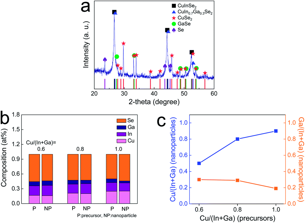 | ||
| Fig. 1 (a) XRD pattern of as-synthesized multiphase, stoichiometric CIGSe nanoparticles, (b) compositions, and (c) elemental analysis of multiphase nanoparticles controlled as a function of the relative concentration between starting precursors in a reaction batch; the atomic ratio of Cu to (In + Ga) is 0.6 to 1.0 with a constant atomic ratio (∼7/3) of In to Ga. | ||
The functional suspension including multiphase CIGSe-based nanoparticles was formulated by incorporating the particles in a solvent mixture of EtOH and EG with an organic additive, PVP. PVP was added for adjusting the rheological properties suitable to a simple bar-coating as well as for facilitating the crack-free absorber layer. For the CIGSe-based ink prepared without PVP, micron-sized cracks formed in the films, having a detrimental effect on the performance of devices.8 The prepared suspensions were deposited on Mo-coated glass substrates using a bar-coating technique, followed by drying at 80 °C and selenization (annealing under a Se atmosphere) at various temperatures. In forming the CI(G)Se absorber layer, the supply of Se vapor during an annealing process is, in general, essential in inducing the microstructural evolution and preventing the formation of (In,Ga)–Se volatile phases. All of the selenized films were free of cracks (Fig. S3†). Fig. 2a shows the crystalline phase evolution of multiphase CIGSe-based particulate films depending on the selenization temperature when it exceeded 300 °C. It was revealed that after selenization at 300 °C, the peaks for secondary phases almost completely disappeared through the phase transformation into the CIGSe phase, leaving behind a small amount of untransformed CuSe phase positioned at 31.06° and 46.00°. As the selenization temperature increased to 550 °C, temperature-dependent crystallization took place, and only the main CIGSe phase existed, indicative of the complete phase transformation of the secondary phases into the CIGSe phase. According to a compositional analysis of the selenized CIGSe-based films (Fig. 2b), the relative composition of each element did not vary regardless of the selenization temperature. This indicates that the prepared multiphase CIGSe-based layer does not undergo a composition change in conjunction with the formation of volatile phases. In many cases, the chalcopyrite nanoparticles underwent a compositional change at an elevated temperature, as the atoms in nanoparticles are not bound strongly enough to prevent the thermal phase-decomposition forming volatile selenide-based binary phases, even under a high vapor pressure Se atmosphere.8,15 The multiphase CIGSe-based nanoparticles prepared in this study are stable against thermally enhanced phase-decomposition reactions, thus allowing for the easy optimization of the selenization process without the complicated consideration on temperature-dependent compositional variation of absorber layers.
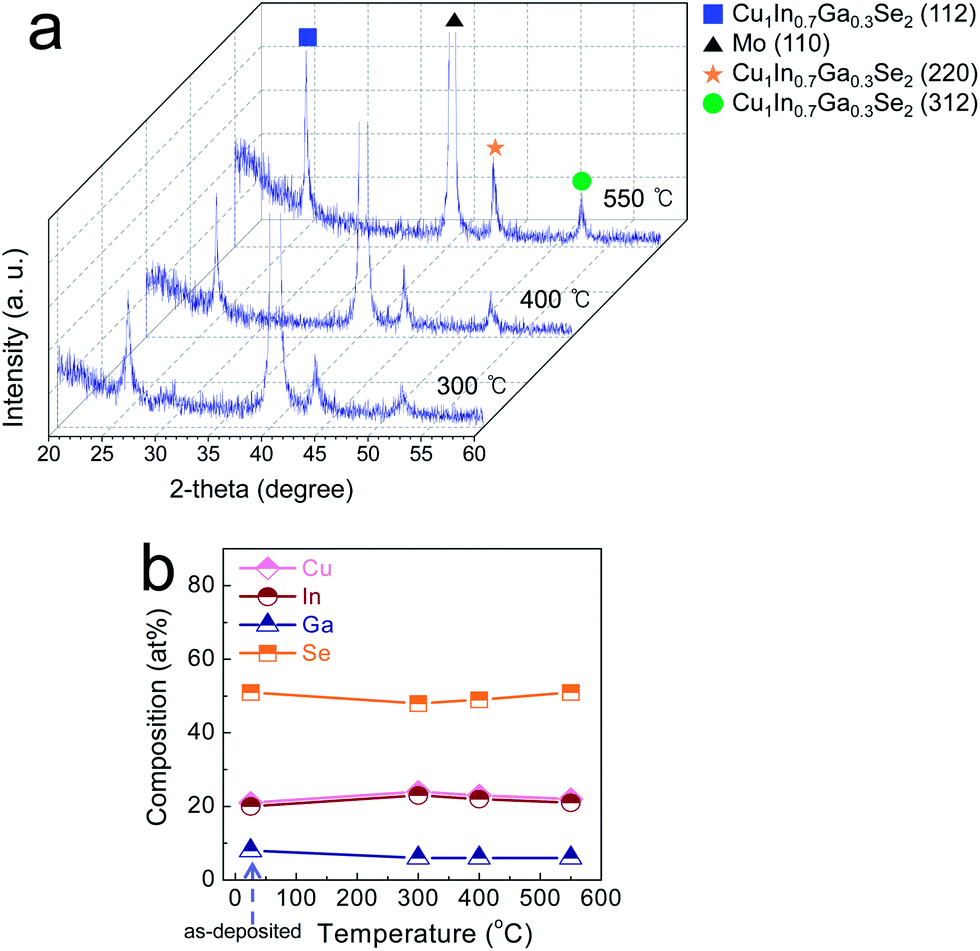 | ||
| Fig. 2 (a) XRD spectra and (b) compositional changes for multiphase CIGSe-based particulate films selenized at 300, 400, and 550 °C. | ||
The microstructural evolutions of multiphase CIGSe-based particulate films are shown in Fig. 3. After selenization at 300 °C, a distinct grain structure did not evolve. In this temperature region, the Se, one of the secondary phases, can melt and act as an active flux material for liquid-phase densification. However, the PVP, incorporated as an organic additive, does not start to decompose at 300 °C (Fig. S4†), which hinders the mass transport between neighboring nanoparticles through a liquid phase, critically interrupting the reactive densification reaction. In contrast, after selenization at 400 °C, at which the thermal decomposition of PVP is partially initiated, grain-like microstructures were observed with a disconnected inter-grain morphology (Fig. 3b). Additionally, at 400 °C, the supply of the additional Se phase, which evolves due to the phase transition of CuSe2 into CuSe/Cu2Se and Se, leads to a more vigorous liquid phase densification process.16 However, while the densification reaction occurs, the PVP is simultaneously decomposed, thus releasing the vaporized organic moieties throughout the film and in turn restricting the inter-connections between the grains. When the multiphase CIGSe-based absorber layer was selenized at 550 °C in order to induce the complete thermal decomposition of PVP as well as the complete melting of the CuSe2 phase prior to the phase transition, a well-crystallized and much denser morphology was obtained. The chalcopyrite films, composed of nanoparticles without low-melting-point secondary phases, do not undergo a densification reaction in any case;7 thus, it is presumed that the low-melting-point phases, Se and CuSe2, incorporated intentionally by tailoring the phase evolution during the synthesis reaction, play a critical role in forming the dense, film-like microstructure. In current research, the prerequisites for generating the more densely packed grain structures are as follows: (i) restriction of the phase transition of secondary phases into the CIGSe phase while reaching the desirable, high selenization temperature, and (ii) selection of an organic additive easily decomposable at a lower temperature. As the temperature increases during the selenization process, the secondary phases are consumed by the partial phase transition into the CIGSe phase, which should be suppressed during the ramping process to induce a vigorous melting-induced densification reaction at 550 °C. Rapid thermal annealing is an alternative means of controlling the reaction path of the secondary phases; however, the absorber layer, incorporating PVP as an organic additive, does not accommodate the thermal shock which occurs with films during a rapid heating/cooling step, resulting in micron-sized cracks on the surface of the films. Thus, organic additives, which release the mechanical stress accumulated inside the films, should be investigated in a future study. As described above, the thermal decomposition behavior of the organic additive is an important factor in determining the lateral microstructural evolution at an elevated temperature. In addition, the remaining organic moieties that have an adverse effect on the densification reactions influence the vertical morphology of the microstructures. Before reaching 550 °C, a slight densification reaction, caused by the subtle melting of the low-melting-point phases, occurs gradually during the ramping process, together with the temperature-dependent thermal decomposition of the PVP. This leads to the trapping of decomposed organic moieties inside a film with a dense, top-surface layer, restricting the densification to the bottom surface of the absorber layer (Fig. S5a†). The presence of undecomposed organic moieties was proven during the examination of the depth compositional profile (Fig. S5b†). For solution-processed CI(G)Se absorber layers, the presence of residue in the bottom layer is usually observed,5 as the carbon-containing components should be incorporated in an ink in the form of an organic additive and/or precursor; moreover, they are not easily eliminated in the final, selenized film. Basic research which attempts to find organic additives that meet the aforementioned prerequisites is currently underway. In addition, the migration of Ga toward a bottom of CIGSe absorber layer was also observed. The Ga migration toward the Mo back contact has been frequently observed during the selenization of metallic precursors, which has been attributed to the difference in reaction rates of Cu–In–Se and Cu–Ga–Se phases.17 The reaction rate between Cu and In is much faster than that between Cu and Ga, resulting in the preferential formation of (Cu,In)–Se phases at a top surface.
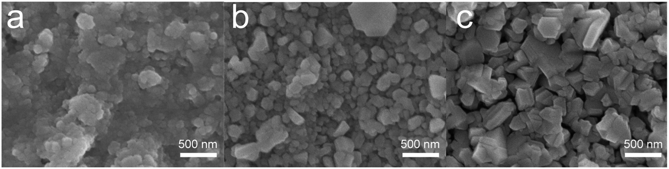 | ||
| Fig. 3 Top-view SEM images for the solution-processed multiphase CIGSe-based particulate films selenized at (a) 300, (b) 400, and (c) 550 °C. All scale bars are 500 nm. | ||
A completely phase-transformed CIGSe absorber layer, selenized at 550 °C, was implemented in a photovoltaic device architecture through the following standard procedures: the chemical bath deposition of CdS (60 nm), the RF sputtering of i-ZnO (50 nm), the RF sputtering of Al-doped n-ZnO (500 nm), and the thermal evaporation of a patterned Al grid as a current collector. An anti-reflection layer was not deposited for the devices tested in this study. Finally, the devices were mechanically scribed into individual cells with an active area of 0.44 cm2. For films selenized at 300 and 400 °C, the reproducible photovoltaic data were not obtainable, owing to the incomplete phase transformation and relatively less dense microstructures. The current–voltage (I–V) characteristics of the photovoltaic device are displayed in Fig. 4a, showing a conversion efficiency of 2.3% with an open-circuit voltage (Voc), a short circuit current density (Jsc), and a fill factor (FF) of 0.29 V, 23.3 mA cm−2, and 33.7%, respectively. According to the external quantum efficiency (EQE) result (Fig. 4b and c), the band gap of CIGSe absorber layer was measured to be 1.18 eV, corresponding to a conventional vacuum-deposited CIGSe layer.18 However, the Voc was quite lower than the values reported for highly-efficient CIGSe solar cells. It was speculated that the Voc is lowered mainly by following factors, including the localized shunting pinholes correlating with the low Rsh value, and the migration of Ga toward the bottom of absorber layer, which reduces the bandgap at a p–n heterojunction.19 Integration of EQE curve of our device yielded Jsc = 19.3 mA cm−2, which is some extent smaller than the Jsc value, 23.3 mA cm−2, obtained from the illuminated I–V curve. It is believed that this small discrepancy can be negligible, taken into consideration the uncertainty in both of the calibrated reference solar cell and the photodiode used to count the number of incident photons.
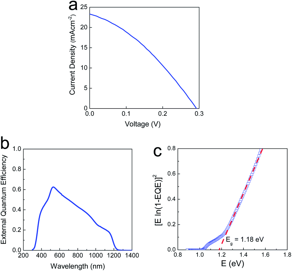 | ||
| Fig. 4 (a) Current–voltage (I–V) characteristics, and (b and c) external quantum efficiency results for the photovoltaic device fabricated using multiphase CIGSe-based particulate films selenized at 550 °C. | ||
The extensive decrease in the EQE within a long-wavelength region was observed, which is attributable to inefficient charge collection through the absorber layer. The photovoltaic device fabricated using multiphase CIGSe-based particulate films selenized at 550 °C suffers from much excessive reduction of EQE compared to that of previously reported one which was fabricated under similar conditions such as nanoparticle-based approach, solution-processed coating and selenization process.5–9 In order to obtain information on the physical quality of our CIGSe layer, we plotted dV/dJ vs. (J + Jsc)−1 from the J–V curve, as shown in Fig. 5. The extracted shunt conductance and series resistance were determined to be 26.5 mS cm−2 and 7.24 Ω cm2, respectively. Compared with our previously-reported, highly efficient, solution-processed CISe solar cell,8 it appeared that the obtained physical parameters show the inferior values. It is believed that the structural imperfection is predominantly attributable to both of the high shunt conductance and the series resistance, besides the contribution of physical defects, commonly considered for explaining the performance degradation in high performance devices. The small voids present between neighboring grains on the top surface of the CIGSe layer would increase the probability of both the CdS and ZnO layer penetrating the CIGSe layer during the chemical bath deposition and sputtering processes.8 Moreover, the formation of an unsuitable interfacial junction adversely influences both physical parameters in conjunction with the carbon-containing residues, limiting the cell performance. However, it should be noted that the multiphase nanoparticles synthesized in this study clearly fulfil several prerequisites as a starting precursor nanoparticle, such as the capability to induce vigorous densification, good composition controllability, thermal stability against phase decomposition at elevated temperatures, and good crystalline structural homogeneity.
 | ||
| Fig. 5 dV/dJ vs. (J + Jsc)−1 from J–V curve for the photovoltaic device fabricated using multiphase CIGSe-based particulate films selenized at 550 °C. Rs value was obtained from the y-intercept of the dV/dJ vs. (J + Jsc)−1 curve, corresponding the y-value when (J + Jsc)−1 = 0, and G value was obtained from a separate dJ/dV vs. V curve.20 | ||
The aforementioned microstructural incompleteness resulted from the undesirable thermal decomposition behavior of the organic additive, which interrupted the effective microstructural evolution inside the particulate films. As an upcoming study, through basic research on the physical/chemical properties of organic additives, the careful selection of a proper organic additive should be carried out, along with its sophisticated incorporation into a suspension containing multiphase CIGSe nanoparticles, after which it is highly likely that the device performance would be greatly improved.
4. Conclusion
In this study, we demonstrated that a microwave-assisted solvothermal synthetic method facilitates the formation of multiphase CIGSe nanoparticles containing the CuSe2 and Se as a low-melting-point phase. Reproducibly-synthesized multiphase nanoparticles enabled for the chemical composition control, from 0.6 to 1.0 in atomic ratio of Cu to (In + Ga), as well as the crystalline structure modulation. It was revealed that the resulting multiphase nanoparticles undergo vigorous liquid-phase densification by triggering the thermally-derived phase transformation of CuSe2 and Se by selenization at 550 °C, which allowed for a relatively dense, homogenous absorber layer with a bilayer-like structure. A photovoltaic device employing a solution-processed CIGSe absorber layer was fabricated, the device performance of which was analytically investigated with calculations of both the shunt conductance and the series resistance.Conflict of interest
The authors declare no competing financial interest.Acknowledgements
This study was supported by a grant from the cooperative R&D program funded by the Korea Research Council of Industrial Science and Technology, and was partially supported by the Industrial Core Technology Development Program, funded by the Ministry of Knowledge Economy (no. 10031709, Development of Direct Nanopatterning Technology for Electronic Devices).References
- V. A. Akhavan, T. B. Harvey, C. J. Stolle, D. P. Ostrowski, M. S. Glaz, B. W. Goodfellow, M. G. Panthani, D. K. Reid, D. A. V. Bout and B. A. Korgel, ChemSusChem., 2013, 6, 481–486 CrossRef CAS PubMed; T. K. Todorov, O. Gunawan, T. Gokmen and D. B. Mitzi, Prog. Photovolt. Res. Appl., 2013, 21, 82–87 CrossRef; S. Rampino, N. Armani, F. Bissoli, M. Bronzoni, D. Calestani, M. Calicchio, N. Delmonte, E. Gilioli, E. Gombia, R. Mosca, L. Nasi, F. Pattini, A. Zappettini and M. Mazzer, Appl. Phys. Lett., 2012, 101, 132107 CrossRef PubMed; M. Yuan, D. B. Mitzi, W. Liu, A. J. Kellock, S. J. Chey and V. R. Deline, Chem. Mater., 2010, 22, 285–287 CrossRef; H.-W. Schock and R. Noufi, Prog. Photovolt. Res. Appl., 2000, 8, 151–160 CrossRef.
- T. K. Todorov, J. Tang, S. Bag, O. Gunawan, T. Gokmen, Y. Zhu and D. B. Mitzi, Adv. Energy Mater., 2013, 3, 34–38 CrossRef CAS; G. Rajesh, N. Muthukumarasamy, E. P. Subramaniam, S. Agilan and D. Velauthapillai, J. Sol-Gel Sci. Technol., 2013, 66, 288–292 CrossRef PubMed; Q. Guo, G. M. Ford, W.-C. Yang, B. C. Walker, E. A. Stach, H. W. Hillhouse and R. Agrawal, J. Am. Chem. Soc., 2010, 132, 17384–17386 CrossRef PubMed; C. Steinhagen, M. G. Panthani, V. Akhavan, B. Goodfellow, B. Koo and B. A. Korgel, J. Am. Chem. Soc., 2009, 131, 12554–12555 CrossRef PubMed.
- M. A. Green, K. Emery, Y. Hishikawa, W. Warta and E. D. Dunlop, Prog. Photovolt. Res. Appl., 2012, 20, 12–20 CrossRef CAS; P. Jackson, D. Hariskos, E. Lotter, S. Paetel, R. Wuerz, R. Menner, W. Wischmann and M. Powalla, Prog. Photovolt. Res. Appl., 2011, 19, 894–897 CrossRef; I. Repins, M. A. Contreras, B. Egaas, C. DeHart, J. Scharf, C. L. Perkins, B. To and R. Noufi, Prog. Photovolt. Res. Appl., 2008, 16, 235–239 CrossRef.
- C. J. Hibberd, E. Chassaing, W. Liu, D. B. Mitzi, D. Lincot and A. N. Tiwari, Prog. Photovolt. Res. Appl., 2010, 18, 434–452 CrossRef CAS; M. Bar, I. Repins, M. A. Contreras, L. Weinhardt, R. Noufi and C. Heske, Appl. Phys. Lett., 2009, 95, 052106 CrossRef PubMed; R. Caballero and C. Guillen, Sol. Energy Mater. Sol. Cells, 2005, 86, 1–10 CrossRef PubMed; G. S. Chen, J. C. Yang, Y. C. Chan, L. C. Yang and W. Huang, Sol. Energy Mater. Sol. Cells, 2009, 93, 1351–1355 CrossRef PubMed.
- A. Cho, S. J. Ahn, J. H. Yun, J. Gwak, S. K. Ahn, K. Shin, H. Song and K. H. Yoon, Sol. Energy Mater. Sol. Cells, 2013, 109, 17–25 CrossRef CAS PubMed; A. R. Uhl, C. Fella, A. Chirila, M. R. Kaelin, L. Karvonen, A. Weidenkaff, C. N. Borca, D. Grolimund, Y. E. Romanyuk and A. N. Tiwari, Prog. Photovolt. Res. Appl., 2012, 20, 526–533 CrossRef; A. Cho, S. J. Ahn, J. H. Yun, J. Gwak, H. Song and K. Yoon, J. Mater. Chem., 2012, 22, 17893–17899 RSC; S. J. Ahn, C. W. Kim, J. H. Yun, J. Gwak, S. Jeong, B.-H. Ryu and K. Yoon, J. Phys. Chem. C, 2010, 114, 8108–8113 Search PubMed.
- S. J. Park, J. W. Cho, J. K. Lee, K. Shin, J.-H. Kim and B. K. Min, Prog. Photovolt. Res. Appl., 2014, 22, 122–128 CrossRef CAS; S. J. Ahn, T. H. Son, A. Cho, J. Gwak, J. H. Yun, K. Shin, S. K. Ahn, S. H. Park and K. H. Yoon, ChemSusChem, 2012, 5, 1773–1777 CrossRef PubMed; E. Lee, S. J. Park, J. W. Cho, J. Gwak, M.-K. Oh and B. K. Min, Sol. Energy Mater. Sol. Cells, 2011, 95, 2928–2932 CrossRef PubMed.
- Y.-H. Seo, B.-S. Lee, Y. Jo, H.-G. Kim, Y. Choi, S. J. Ahn, K. H. Yoon, K. Woo, J. Moon, B.-H. Ryu and S. Jeong, J. Phys. Chem. C, 2013, 117, 9529–9536 CAS; Y.-H. Seo, B.-S. Lee, Y. Jo, H.-G. Kim, K. Woo, J. Moon, Y. Choi, B.-H. Ryu and S. Jeong, ACS Appl. Mater. Interfaces, 2013, 5, 6930–6936 Search PubMed.
- S. Jeong, B.-S. Lee, S. J. Ahn, K. H. Yoon, Y.-H. Seo, Y. Choi and B.-H. Ryu, Energy Environ. Sci., 2012, 5, 7539–7542 CAS.
- C. Kind, C. Feldmann, A. Quintilla and E. Ahlswede, Chem. Mater., 2011, 23, 5269–5274 CrossRef CAS.
- M. G. Panthani, V. Akhavan, B. Goodfellow, J. P. Schmidtke, L. Dunn, A. Dodabalapur, P. F. Barbara and B. A. Korgel, J. Am. Chem. Soc., 2008, 130, 16770–16777 CrossRef CAS PubMed.
- S.-J. L. Kang, Sintering: Densification, Grain Growth, and Microstructure, Elsevier Ltd, 2005, pp. 9–18, ISBN 978-0-7506-6385-4 CrossRef CAS PubMed; R. M. German, P. Suri and S. J. Park, J. Mater. Sci., 2009, 44, 1–39 CrossRef CAS PubMed.
- Q. Guo, G. M. Ford, R. Agrawal and H. W. Hillhouse, Prog. Photovolt. Res. Appl., 2013, 21, 64–71 CrossRef CAS; Q. Guo, G. M. Ford, H. W. Hillhouse and R. Agrawal, Nano Lett., 2009, 9, 3060–3065 CrossRef PubMed; U. Rau, M. Schmitt, F. Engelhardt, O. Seifert, J. Parisi, W. Riedl, J. Rimmasch and F. Karg, Solid State Commun., 1998, 107, 59–63 CrossRef.
- S. Jeong, S. H. Lee, Y. Jo, S. S. Lee, Y.-H. Seo, B. W. Ahn, G. Kim, G.-E. Jang, J.-U. Park, B.-H. Ryu and Y. Choi, J. Mater. Chem. C, 2013, 1, 2704–2710 RSC; S. Jeong, H. C. Song, W. W. Lee, H. J. Suk, S. S. Lee, T. Ahn, J.-W. Ka, Y. Choi, M. H. Yi and B.-H. Ryu, J. Mater. Chem., 2011, 21, 10619–10622 RSC; S. Jeong, H. C. Song, W. W. Lee, Y. Choi, S. S. Lee and B.-H. Ryu, J. Phys. Chem. C, 2010, 114, 22277–22283 Search PubMed; S. Jeong, H. C. Song, W. W. Lee, Y. Choi and B.-H. Ryu, J. Appl. Phys., 2010, 108, 102805-1–102805-5 CrossRef CAS PubMed.
- A. Gloskovskii, C. A. Jenkins, S. Ouardi, B. Balke, G. H. Fecher, X.-F. Dai, T. Gruhn, B. Johnson, I. Lauermann, R. Caballero, C. A. Kaufmann and C. Felser, Appl. Phys. Lett., 2012, 100, 092108 CrossRef CAS PubMed; M. Ruckh, D. Schmid, M. Kaiser, R. Schaffler, T. Walter and H. W. Schock, in Proc. 1st World Conf. Photovolt. Energy Conv., IEEE, New York, 1994, vol. 156 CrossRef; R. Herberholz, H. W. Schock, U. Rau, J. H. Werner, T. Haalboom, T. Godecke, F. Ernst, C. Beilharz, K. W. Benz and D. Cahen, in Proc. 26th IEEE Photovoltaic Specialists Conference, IEEE, Piscataway, NJ, 1998, vol. 323 CrossRef; R. Herberholz, U. Rau, H. W. Schock, T. Haalboom, T. Godecke, F. Ernst, C. Beilharz, K. W. Benz and D. Cahen, Eur. Phys. J.: Appl. Phys., 1999, 6, 131 CrossRef.
- C. J. Hibberd, K. Ernits, M. Kaelin, U. Muller and A. N. Tiwari, Prog. Photovolt. Res. Appl., 2008, 16, 585–593 CrossRef CAS; F. Hergert, R. Hock, A. Weber, M. Purwins, J. Palm and V. Probst, J. Phys. Chem. Solids, 2005, 66, 1903–1907 CrossRef PubMed.
- S. Yoon, T. Yoon, K.-S. Lee, S. Yoon, J. M. Ha and S. Choe, Sol. Energy Mater. Sol. Cells, 2009, 93, 783–788 CrossRef CAS PubMed.
- M. Marudachalam, R. W. Birkmire, H. Hichri, J. M. Schultz, A. Swartzlander and M. M. Al-Jassim, J. Appl. Phys., 1997, 82, 2896–2905 CrossRef CAS PubMed.
- T. Minemoto, Y. Hashimoto, W. Shams-Kolahi, T. Satoh, T. Negami, H. Takakura and Y. Hamakawa, Sol. Energy Mater. Sol. Cells, 2003, 75, 121–126 CrossRef CAS; T. Dullweber, G. Hanna, U. Rau and H. W. Schock, Sol. Energy Mater. Sol. Cells, 2001, 67, 145–150 CrossRef; S. H. Wei and A. Zunger, J. Appl. Phys., 1995, 78, 3846–3856 CrossRef PubMed.
- V. K. Kapur, A. Bansal, P. Le and O. I. Asensio, Thin Solid Films, 2003, 431–432, 53–57 CrossRef CAS; W. Guo and B. Liu, ACS Appl. Mater. Interfaces, 2012, 4, 7036–7042 Search PubMed.
- S. S. Hegedus and W. N. Shafarman, Prog. Photovolt. Res. Appl., 2004, 12, 155–176 CrossRef CAS.
Footnote |
| † Electronic supplementary information (ESI) available: SEM image, STEM image and TEM-EDS compositional profiles of the as-synthesized multiphase CIGSe nanoparticles, XRD spectra of the as-synthesized CIGSe nanoparticles in multiple experiments with identical synthetic conditions to assess the reproducibility of the result, top-view optical microscope images of the solution-processed multiphase CIGSe-based particulate films selenized at 300, 400, and 550 °C, TGA results for the PVP, and cross-sectional SEM images and AES depth profiles of solution-processed multiphase CIGSe-based particulate films selenized at 550 °C. See DOI: 10.1039/c4ra00623b |
| This journal is © The Royal Society of Chemistry 2014 |