Optimization of silicon pyramidal emitter by self-selective Ag-assisted chemical etching
Lixia Yangab,
Yaoping Liu*ab,
Yan Wangab,
Xiuqing Lic,
Wei Chenab,
Yongyun Huac,
Qinjie Zhangc,
Jianqi Fuc,
Huili Liangab,
Zengxia Mei*ab and
Xiaolong Duab
aBeijing National Laboratory for Condensed Matter Physics, Institute of Physics, Chinese Academy of Sciences, Beijing 100190, China. E-mail: ypliu@aphy.iphy.ac.cn; zxmei@aphy.iphy.ac.cn
bKey Laboratory for Renewable Energy, Chinese Academy of Science, Beijing Key Laboratory for New Energy Materials and Devices, Beijing 100190, China
cBeijing Flight Boda Electronics Ltd, No. 247 Ma Fang West Industrial Park Pinggu District, Beijing 101204, China
First published on 20th May 2014
Abstract
Optimization of a silicon pyramidal emitter by self-selective Ag-assisted chemical etching is explored with regard to solar cell applications. Increased sheet resistance and increased lifetime of the minority carriers together indicate that the emitter recombination is significantly reduced, as a result of minimizing the dead layer on the silicon surface. Scanning electron microscopy (SEM) images reveal that the peaked pyramid becomes rounded, alleviating the heavy phosphorus (P) diffusion at the peak of the pyramid. Moreover, the reflectivity of the silicon wafers increases a little after optimization due to the formation of the rounded pyramids, indicating that the emitter becomes more uniform as well. Such an optimization process will result in a minimized dead layer and uniform emitter, leading to decreased Auger recombination and enhanced efficiency of collecting electrons, which improves the open-circuit voltage (Voc), short-circuit current density (Jsc), conversion efficiency (Eff) and external quantum efficiency (EQE) of the solar cells significantly.
1. Introduction
For crystalline silicon solar cells, an n+-type emitter is generally formed by thermal diffusion of P from a phosphorus oxychloride (POCl3) source in a furnace. The resulting P diffusion profile exhibits a very high concentration near the surface, and it is well known that high concentrations of P that exceed the solid solubility limit form phosphorous precipitates that function as defects to cause the excess dopant to become electrically inactive, which results in increased recombination and poor blue-spectrum response.1–6 This layer with high concentrations of P, known as the dead layer, can be minimized by changing the diffusion parameters, such as the flow rate of POCl3, the diffusion temperature and the duration of diffusion. Thus, by thinning the dead layer, a shallow junction with a high sheet resistance is achieved, the emitter recombination is reduced and the blue-spectrum response is enhanced. This will result in higher Voc and Jsc.In order to optimize the P concentration profile and minimize the dead layer, a pre-oxidation step is introduced prior to P diffusion.2,7,8 A thin oxide layer resulting from the pre-oxidation will consume part of the dead layer during the subsequent diffusion, and then the oxide and phosphorus silicate glass (PSG) layer are removed in diluted HF at the end of the diffusion process.2 Nevertheless, the pre-oxidation is usually carried out at about 825 °C for 10–60 min. The high temperature process is high-cost, and it is detrimental to the lifetime of bulk silicon.
On the other hand, post-chemical treatments, such as HF dipping,1 alkali treatment9,10 and HNO3/HF vapor etching,11 are effective and low-cost for removing the dead layer. However, pyramidal emitters are not uniform; they show a deeper junction at the peak and a shallower junction at the valley. Young-Woo Ok et al. demonstrated that the formation of a nonuniform junction profile in a textured silicon surface is associated with the dependence of P diffusion on the inhomogeneous distribution of silicon interstitials caused by the geometry of the pyramid texture.12 The nonuniformity of the emitter leads to a low efficiency of collecting electron, resulting in a low Jsc and degraded solar cell performance.13 Although the above post-chemical treatments can minimize the dead layer and modify the emitter profile, it cannot offset the difference of the junction depth at the peak and valley. Therefore a controllable selective treatment technique that can both remove the dead layer and alleviate the nonuniformity of the junction is needed.
In our previous study, we noted that the etching rate is faster at the kinks and steps of multicrystalline silicon's ‘worm like’ structure than in other areas when we used the Ag-assisted chemical etching method to produce black silicon. The nanostructures that form near steps are deeper than those in the flat areas.14 Due to more serious surface recombination and insufficient passivation in these deeper nanostructures at the steps and kinks, the performance of those black-silicon-based solar cells was worse than expected. However, this behavior inspired us to try self-selective chemical etching on a pyramidal emitter. Then, by a combination of the self-selective Ag-assisted chemical etching and KOH etching treatment, a pyramidal emitter with a minimized dead layer, uniform junction depth and high sheet resistance was obtained, with a reduced emitter recombination and enhanced blue-spectrum response, contributing to higher Eff, Voc and Jsc for the cells.
2. Experimental details
Commercial 156 mm × 156 mm (100)-oriented silicon, boron-doped (1–3 Ω cm) p-type wafers were used in the study. The silicon wafers were first pyramid-textured15,16 (anisotropic etching of silicon in aqueous alkaline solutions with 3 wt% NaOH, 10 wt% IPA and 1 wt% texture additive, 80 °C, 20 min) and thoroughly rinsed by the conventional process, and then underwent conventional homogeneous P diffusion, which yielded a sheet resistance of 50 Ω sq−1 with a deviation of less than 1.98 Ω sq−1. The PSG was removed with HF (10 vol%) for 1 min. Then self-selective Ag-assisted chemical etching and KOH etching were carried out to modify the silicon pyramidal emitter. First, the P-diffused silicon wafers were immersed in a mixture of 0.005 M AgNO3 and 1.15 M HF for 20 s, 30 s and 40 s, labeled as sample A, B and C, respectively. Second, residual Ag nanoparticles were removed by nitric acid dipping for 20 min. Then, the nanostructures formed on the sample A, B and C were removed in 2 wt% KOH and 5 wt% IPA for 3 min. All the above chemical treatments were performed at room temperature. Afterward, the samples went through rigorous RCA3 cleaning to remove any metallic contaminants from the surface. Finally, the optimized and reference solar cells (labeled as sample R) were fabricated via a conventional solar cell process.The morphologies and structures of the samples were characterized with a Hitachi S-4800 scanning electron microscope. Hemispheric total reflectance for normal incidence was measured on a Varian Cary 5000 spectrophotometer with an integrating sphere. The lifetime of the minority carriers was measured by using a Semilab WA-200. The cell efficiency was measured by using a BERGER Lichttechnik Single Cell Tester and EQE was measured by using a Solar Cell Spectral Response/QE/IPCE Measurement System QEX10.
3. Results and discussion
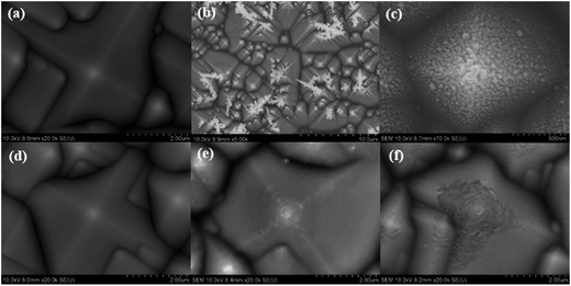
The SEM of sample R (shown in Fig. 1(a)) demonstrates that the peak of the pyramid is pointed, which makes a deeper junction due to the heavier P diffusion that results from the peak geometry. Fig. 1(b) is an SEM image of sample B, showing that bigger and more Ag nanoparticles are adsorbed at the peaks than in the valleys of the pyramids, which induces a faster etching rate. This is an electrochemical reaction between silicon and Ag+/Ag, the mechanism of Ag-assisted chemical etching has been discussed in our previous works.14,17,18 In Fig. 2, we present a simplified model for the mechanism of the self-selective deposition of Ag nanoparticles on pyramidal structures. The surface free energy (SFE) of crystal faces is proportional to the number of bonds on the surface.19 For crystalline silicon, surface properties depend on the orientation of crystal lattice, silicon (100) has higher surface bond density, while silicon (111) has a lower surface bond density; therefore silicon (100) has a higher SFE than silicon (111),19,20 which makes silicon (100) more active than silicon (111). Moreover, SFE is much higher at the peaks and kinks than at the flat areas, which makes these regions more active. The electrons in these regions are more active due to the higher SFE, therefore Ag+ ions will capture electrons from here and adsorb preferentially, covering the peaks and decreasing the SFE. The Ag nanoparticles tend to form at the kinks, steps, and other defects first, in agreement with the principle of lowest energy and in accordance with our previous work.14 The adsorbed Ag nanoparticles restrict the oxidation of the silicon surface, and the etching process occurs only on the silicon underneath the Ag nuclei. So these are the reasons that lead to the self-selective surface etching of the peaks and valleys of the pyramidal emitter. The reaction can be described as two half-cell reactions.21–23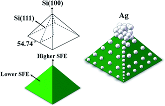 | ||
| Fig. 2 A simplified surface free energy (SFE) model for the mechanism of self-selective deposition of Ag nanoparticles. | ||
Cathode reaction:
| Ag+ + eVB− → Ag0 (s) |
Anode reaction:
| Si (s) + 2H2O → SiO2 + 4H+ + 4eVB− |
| SiO2 (s) + 6HF → H2SiF6 + 2H2O |
As the etching time increases, the depth of the nanostructures becomes deeper and the etching difference between the peak and the valley of the pyramid becomes more significantly. Fig. 1(c) is a high resolution image of Fig. 1(b). After removing the Ag nanoparticles and the nanostructures, rounded pyramids are revealed, as shown in Fig. 1(d–f), which indicates that the junction depth has been made more uniform by etching the peaks off, and the heavier P diffusion, which resulted from the peak geometry, is alleviated.
Meanwhile, besides rounding the pyramids, the other key result of the etching process is a uniform and suitable sheet resistance. The sheet resistance of the silicon wafer is 50 Ω sq−1 after conventional P diffusion, and then it increases to 63 Ω sq−1, 78 Ω sq−1 and 83 Ω sq−1 when the etching time increases from 20 s to 40 s, which indicates a decrease of P concentration on the silicon surface. This is attributed to the etching of rounded pyramids. In addition, the lifetime of minority carriers is 5.38 μs for sample A, 6.38 μs for sample B and 5.6 μs for sample C – all higher than that for sample R, which is 5.15 μs. We attribute the increased lifetime to the reduced Auger recombination, arising from the reduced concentration of P on the silicon surface. The relationship between Auger lifetime and the concentration of both majority carriers and minority carriers for an n-type emitter is:24
| τAug = 1/(Cnp + Dn2), | (1) |
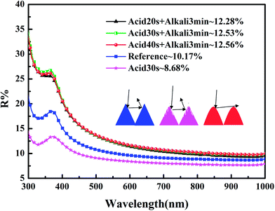
As can be observed in Fig. 3, the reflectivity of the etched wafers is a little lower than the reference wafer's because of the nanostructures formed on the pyramids – such a density-graded silicon layer can suppress surface reflection.25 Removing the nanostructures increases the reflectivity, making it higher than that of the reference, due to the roundness of the pyramids and the elimination of secondary reflections. This phenomenon indicates that the junction depth is made uniform as well.
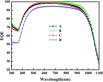
As we mentioned above, the poor blue-spectrum response is due to the dead layer. This is confirmed by the EQE measurements of cells, as shown in Fig. 4. Sample R has a relatively low EQE, this is because of the high Auger recombination rate, resulting from the thick dead layer. After optimizing, as can be observed, the EQE improves over the whole wavelength range from 300 nm to 1100 nm, and the blue-spectrum response is greatly improved. These improvements indicate that the dead layer is minimized effectively, and therefore the Auger recombination is decreased significantly.
Measurements with a BERGER Lichttechnik Single Cell Tester show that the Eff of sample B with a 78 Ω sq−1 sheet resistance is 18.83%, with a 639.27 mV Voc, a 37.20 mA cm−2 Jsc and a 79.10% fill factor (FF), as shown in Table 1. Compared to the reference, the optimized solar cells are significantly improved in Voc, Jsc and Eff. The increased Voc results from a high sheet resistance and a reduced Auger recombination. The increase in Jsc is mainly attributed to the reduced Auger recombination and the more uniform junction, which will enhance the collection efficiency of the electrons. Fig. 5 shows the emitter profile and energy band schematic diagram before and after optimization, which illustrates the reason for the increased efficiency of collecting electrons. As mentioned above, the pyramidal emitter is not uniform, showing a deeper junction at the peak and a shallower junction in the valley. That is, the layer is n+-type at the peaks and n-type at the valleys. At the peak, a strong vertical electric field E1⊥ is formed from n+-type layer to p-type layer, while at the valley, a weak vertical electric field E2⊥ is formed from n-type layer to p-type layer; then a lateral electric field E∥ from n+-type layer to n-type layer is formed. The transport and collection of the electrons are not only governed by E1⊥ and E2⊥, but are also influenced by E∥.26 Hereby, the electrons will be easily attracted to the peaks of the pyramids, which does not favor the collection of the electrons. As the absence of the electrode on pyramids at the work area of the silicon surface, the electrons have to move along the surface laterally and transport to the electrode area, then the electrons will be collected by the electrode. After optimization, the emitter becomes more uniform and the n+-type layer becomes thinner. As shown in Fig. 5(b), the E′∥ resulting from the difference of E′1⊥ and E′2⊥ becomes so weak that it has only a little influence on the transport and collection of electrons. In this case, it is easier for electrons to move along the surface laterally and to be collected by the electrode, which will enhance the efficiency of collecting electrons. Finally, the conversion efficiency is improved significantly, thanks to the increased Voc and Jsc.
| Sample | Voc (mV) | Jsc (mA cm−2) | FF (%) | Eff (%) |
|---|---|---|---|---|
| A | 638.22 | 37.10 | 79.00 | 18.73 |
| (638.31) | (37.18) | (79.05) | (18.79) | |
| B | 639.03 | 37.08 | 79.13 | 18.78 |
| (639.27) | (37.20) | (79.10) | (18.83) | |
| C | 635.21 | 37.00 | 79.02 | 18.60 |
| (636.35) | (36.92) | (79.11) | (18.61) | |
| R | 626.15 | 34.91 | 79.75 | 17.46 |
| (626.64) | (34.88) | (79.83) | (17.47) |
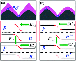 | ||
| Fig. 5 The profile of the emitter and energy band diagram of solar cells (a) before and (b) after optimization. | ||
As shown in the Table 1, the sample B, with 30 s etching, shows the best performance, which means that minimizing the dead layer and decorating the junction depth are indeed enhancements. During its shorter etching time, sample A's morphology changed only slightly, as shown in Fig. 1(a) and (d). Although modifying the junction depth is not enough, the performance of sample A is still better than that of the reference. This is also attributed to the reduced Auger recombination, which is due to the thinned dead layer. The 40 s-etched sample C has the worst performance compared with sample A and B, because of the excessive etching of the pyramidal emitter. As shown in Fig. 1(f), the convex regions of the pyramid experienced a deeper etching, and are not as smooth as sample A and B after etching by KOH/IPA – the rough surface will increase surface recombination. On the other hand, over-etching will result in a higher and inhomogeneous sheet resistance. In this case, the efficiency of collecting electrons will be decreased by the worsening Ohmic contact caused by the higher and inhomogeneous sheet resistance. Even so, the performance of sample C is still better than that of the reference, which suggests that the dead layer and the nonuniformity of the pyramidal emitters have very bad effects on the performance of the solar cell.
4. Conclusions
In conclusion, a silicon pyramidal emitter has been successfully optimized by combining self-selective Ag-assisted chemical etching and KOH etching. The sheet resistance and lifetime of the minority carriers increase due to the dead layer is significantly decreased and consequently, the emitter recombination is also reduced. SEM and optical reflectance measurements indicate that a uniform emitter is formed because the peak of the pyramid is etched off and the heavier P diffusion, which results from the peak geometry, is alleviated. Compared to the reference solar cell, the conversion efficiency of the optimized solar cell is significantly improved, thanks to the increased Voc and Jsc. Decreased Auger recombination results from the minimized dead layer leads to an increase in Voc. In addition, the uniform emitter improves the efficiency of collecting electrons, which leads to the increased Jsc together with the decreased Auger recombination. Finally, the best solar cell, with a conversion efficiency of 18.83%, is obtained. This simple, low-cost optimization process opens new perspectives for high efficiency silicon solar cell applications.Acknowledgements
This work was supported by the Ministry of Science and Technology (Grant no. 2011CB302002, 2009CB929404) of China, the National Science Foundation (Grant no. 11174348, 61076007, 61204067, 11274366, 51272280, 61306011).Notes and references
- H. J. Lee, M. G. Kang, S. J. Choi, G. H. Kang, J. M. Myoung and H. E. Song, Curr. Appl. Phys., 2013, 13, 1718 CrossRef PubMed.
- B. Bazer-Bachi, E. Fourmond, P. Papet, L. Bounaas, O. Nichiporuk, N. Le Quang and M. Lemiti, Sol. Energy Mater. Sol. Cells, 2012, 105, 137 CrossRef CAS PubMed.
- S. Solmi and D. Nobili, J. Appl. Phys., 1998, 83, 2484 CrossRef CAS PubMed.
- D. Nobili, A. Armigliato, M. Finetti and S. Solmi, J. Appl. Phys., 1982, 53, 1484 CrossRef CAS PubMed.
- A. Armigliato, D. Nobili, M. Servidori and S. Solmi, J. Appl. Phys., 1976, 47, 5489 CrossRef CAS PubMed.
- P. Kittidachachan, T. Markvart, G. J. Ensell, R. Greef and D. M. Bagnall, Conference Record of the 31th IEEE Photovoltaic Specialists Conference, January 2005 Search PubMed.
- H. Ghembaza, A. Zerga and R. Saïm, Energy Procedia, 2012, 18, 733 CrossRef CAS PubMed.
- K. D. Shetty, M. B. Boreland, V. Shanmugam, J. Cunnusamy, C. K. Wu, S. Iggo and H. Antoniadis, Energy Procedia, 2013, 33, 70 CrossRef CAS PubMed.
- Y. R. Jiang, R. P. Qing, H. G. Yang, C. Chen, H. Ma and F. G. Chang, Appl. Phys. A, 2013, 113, 13 CrossRef CAS.
- M. Algasinger, J. Paye, F. Werner, J. Schmidt, M. S. Brandt, M. Stutzmann and S. Koynov, Adv. Energy Mater., 2013, 3, 1068 CrossRef CAS.
- M. Saadoun, M. F. Boujmil, S. Aouida, M. B. Rabha and B. Bessaïs, Phys. Status Solidi C, 2011, 8, 1869 CrossRef CAS.
- Y. W. Ok, A. Rohatgi, Y. H. Kil, S. E. Park, D. H. Kim, J. S. Lee and C. J. Choi, IEEE Electron Device Lett., 2011, 32, 351 CrossRef CAS.
- S. Kwon, J. Yi, S. Yoon, J. S. Lee and D. Kim, Curr. Appl. Phys., 2009, 9, 1310 CrossRef PubMed.
- Y. P. Liu, T. Lai, H. L. Li, Y. Wang, Z. X. Mei, H. L. Liang, Z. L. Li, F. M. Zhang, W. J. Wang, A. Y. Kuznetsov and X. L. Du, Small, 2012, 8, 1392 CrossRef CAS PubMed.
- E. Vazsonyi, K. De Clercq, R. Einhaus, E. Van Kerschaver, K. Said, J. Poortmans, J. Szlufcik and J. Nijs, Sol. Energy Mater. Sol. Cells, 1999, 57, 179 CrossRef CAS.
- P. K. Singh, R. Kumar, M. Lal, S. N. Singh and B. K. Das, Sol. Energy Mater. Sol. Cells, 2001, 70, 103 CrossRef CAS.
- Y. Wang, Y. P. Liu, H. L. Liang, Z. X. Mei and X. L. Du, Phys. Chem. Chem. Phys., 2013, 15, 2345 RSC.
- Y. Wang, Y. P. Liu, T. Lai, H. L. Liang, Z. L. Li, Z. X. Mei, F. M. Zhang, A. Kuznetsov and X. L. Du, RSC Adv., 2013, 3, 15483 RSC.
- R. Shuttleworth, Proc. Phys. Soc., London, Sect. A, 1950, 63, 445 CrossRef.
- P. J. Hesketh, C. Ju, S. Gowda, E. Zanoria and S. Danyluk, J. Electrochem. Soc., 1993, 140, 1080 CrossRef CAS PubMed.
- Z. P. Huang, N. Geyer, P. Werner, J. D. Boor and U. Gösele, Adv. Mater., 2011, 23, 285 CrossRef CAS PubMed.
- K. Q. Peng, J. J. Hu, Y. J. Yan, Y. Wu, H. Fang, Y. Xu, S. T. Lee and J. Zhu, Adv. Funct. Mater., 2006, 16, 387 CrossRef CAS.
- K. Q. Peng, H. Fang, J. J. Hu, Y. Wu, J. Zhu, Y. J. Yan and S. T. Lee, Chem.–Eur. J., 2006, 12, 7942 CrossRef CAS PubMed.
- J. I. Pankove, Optical Processes in Semiconductors[M], N. J. Prentice-Hall, Englewood Cliffs, 2012, p. 1971 Search PubMed.
- S. K. Srivastava, D. Kumar, Vandana, M. Sharma, R. Kumar and P. K. Singh, Sol. Energy Mater. Sol. Cells, 2012, 100, 33 CrossRef CAS PubMed.
- Z. N. Shen, B. W. Liu, Y. Xia, J. Liu, J. H. Liu, S. H. Zhong and C. B. Li, Scr. Mater., 2013, 68, 199 CrossRef CAS PubMed.
| This journal is © The Royal Society of Chemistry 2014 |

