DOI:
10.1039/C4RA08343A
(Paper)
RSC Adv., 2014,
4, 54388-54397
Investigations on phosphorous doped hydrogenated amorphous silicon carbide thin films deposited by a filtered cathodic vacuum arc technique for photo detecting applications
Received
8th August 2014
, Accepted 16th October 2014
First published on 16th October 2014
Abstract
This paper reports the growth and properties of phosphorous doped hydrogenated amorphous silicon carbide (P doped a-SiC:H) thin films deposited at room temperature by a filtered cathodic vacuum arc (FCVA) technique using a phosphorous doped solid silicon target as a cathode in the presence of acetylene gas. These films have been characterized by X-ray diffraction (XRD), scanning electron microscopy, energy dispersive X-ray analysis, dark conductivity, activation energy, optical band gap, secondary ion mass spectroscopy, Raman spectroscopy, current–voltage, capacitance–voltage and photoconductive measurements. XRD results exhibit predominantly an amorphous phase for the films. The effect of the arc current on the properties of P doped a-SiC:H films have been studied. A P doped a-SiC:H/c-Si heterojunction diode was fabricated which showed a diode ideality factor between 1.5 to 1.7 and the density of states were 9.6 × 10¹⁶ to 4.8 × 1017 cm−3 eV−1. The photo response behaviors of the P doped a-SiC:H films have been tested by measuring the change in the electrical resistance on light illumination with the fast response and recovery time as 7.8 to 9.5 and 6.2 to 12.8 s, respectively. The P doped a-SiC:H film deposited at a 30 A arc current has shown a photo response of ∼1.6% at an illumination intensity of ∼100 mW cm−2.
1. Introduction
Hydrogenated amorphous silicon carbide (a-SiC:H), considered as one of the most promising thin-film materials exhibits unique physical, chemical, electronic and optical properties1 and has a variety of promising technological applications2 in thin film photovoltaic devices,3 thin film transistors, image sensors, etc. The applications may range from the protective layer of solar cells for both the crystalline and thin films4 to microelectronic nanomechanical devices5 and from the passivation layer to lithium ion batteries.6 Silicon carbide is also used as a substrate in the catalyst free growth of graphene by many researchers.7 The other interesting applications of a-SiC:H films are antireflection coating for solar cells, as dielectric, color sensor, scanning probe and supercapacitor applications.8 Yunaz et al.9 used a-SiC:H films in the multijunction solar cells.
The a-SiC:H thin film in photovoltaic (PV) technology is experiencing a dramatic growth curve worldwide and offers an obliging business opportunity in the power generation and building integrated solutions with the cost effective, product maturity, excellent reliability and availability of the product in large volume. In particular, a-SiC:H has inspired technological interest due to the possibility of tailoring its physical properties to suit different applications by varying the relative composition of constituent atoms. It is the beauty of a-SiC:H thin film material that the composition of constituent atoms can be easily controlled by its growth parameters.1 Hybrid silicon carbon nanostructure composites are used as anode for lithium ion batteries.10 Phosphorus-doped amorphous silicon carbide (a-SiC:H) also demonstrated the ability to passivate the c-Si substrates and highly doped n-type emitters in the solar cells.11 a-SiC:H provides the excellent electronic surface passivation for the crystalline silicon solar cells.
So far, the production of a-SiC:H thin films have been focused on some deposition techniques such as plasma enhanced chemical vapor deposition (PECVD),12 hot wire chemical vapor deposition (HWCVD),13 electron cyclotron resonance chemical vapor deposition (ECR-CVD)14 etc. These processes require the dilution of silane gas with the hydrogen at a relatively high substrate temperature and high pressure for the growth of the film. Filtered cathodic vacuum arc (FCVA) technique has been used earlier to deposit amorphous silicon thin films.15,16 This technique has also been used to deposit boron doped tetrahedral amorphous carbon (ta-C) film as a window layer in the inline production of large area amorphous silicon solar cell for improving the efficiency.17 In this technique, the properties of the grown film can be controlled by the various process parameters such as arc current, substrate temperature, substrate bias, and gaseous pressure used in the reactive mode. For the growth of a-SiC:H thin film using these conventional processes, a mixture of SiH4 and CH4 gases and for the doping purpose B2H6 and PH3 gases are used. Moreover, the SiH4 gas employed in the growth of the film is flammable and the doping gases like B2H6 and PH3 are highly toxic in nature. Thus, a proper solution to this problem is to grow these thin films from the solid silicon target without introducing any toxic gases in the deposition chamber and now researchers18 have started thinking in this direction also. Shi et al.19 deposited amorphous silicon carbon (a-SiC) films by FCVA technique and studied their structural properties by the AFM, Raman and XRD measurements. Srisang et al.20 reported SiC formation and characterization at the interface of DLC/a-Si films prepared by the pulsed FCVA technique. Demichelis et al.21 reported in their work that the acetylene plasma is suitable to grow a-SiC:H films having a high band gap, high uniformity and high deposition rate compared to that of CH4 plasma. Giorgis et al.22 suggested acetylene as a better carbon source which overcomes the structure related degradation of electronic properties of methane used a-SiC:H films.
One of the key inspirations for this paper has been the development of environmentally friendly, non toxic and non hazardous deposition technique for the growth of P doped a-SiC:H thin film materials for various electronic applications. We report the growth and properties of P doped a-SiC:H thin film deposited by the FCVA process by employing a phosphorous doped Si ingot as a cathode and graphite rod as an anode in the presence of acetylene gas. One of the advantages of the FCVA process in the deposition of a-SiC:H thin film is that no toxic and hazardous gases like SiH4, PH3 and B2H6 have been used and it is a high rate deposition process also. The effect of arc current on the structural, electrical and optical properties of P doped a-SiC:H films have been studied. The deposited films have been characterized by X-ray diffraction (XRD), scanning electron microscope (SEM), energy dispersive X-ray analysis (EDAX), Raman spectroscopy, secondary ion mass spectroscopy (SIMS), electrical, optical and photoconductive properties. The current–voltage (I–V) and capacitance–voltage (C–V) measurements of the heterojunction structure have also been measured. The P doped a-SiC:H film show photo detection with the fast response and recovery time.
2. Experimental
2.1. FCVA technique and deposition of the film
A custom designed and indigenously developed FCVA system23–26 has been used to deposit P doped a-SiC:H thin film in the presence of acetylene (C2H2) gas. The DC arc supply used was capable of delivering arc current up to 200 A. The FCVA process is based on striking the arc (arc voltage of 35–40 V) with an arc current of 30–100 A between the two electrodes. Here, one electrode is P doped silicon ingot of (resistivity 0.55 Ω cm) 50 mm diameter and 5 mm thickness as cathode (purity 99.999%), that works as a silicon source in order to deposit P doped a-SiC:H films. Second electrode is a retractable high purity graphite rod of 7 mm dia. (purity 99.999%) as a striker. Acetylene gas of purity 99.999% was introduced in the chamber which was used as a carbon source. The magnetic filter is energized using direct current source (D.C.) power supply and a magnetic field of ∼350 G is achieved inside the duct to remove the macro particles generated during the arcing. The P doped a-SiC:H thin films were deposited on 7059 glass and silicon substrate placed at a distance of ∼35 cm away from the cathode. Prior to the deposition, the chamber is evacuated to a base pressure of around ∼10−6 mbar. The films are deposited sequentially for 5 s and then cooled for 50 s in a pulsating nature. In this work, a series of samples were deposited by varying the arc current from 30 to 100 A at room temperature. The pressure used during the arc was ∼5.4 × 10⁻² mbar using C2H2 gas.
2.2. Details of measurements
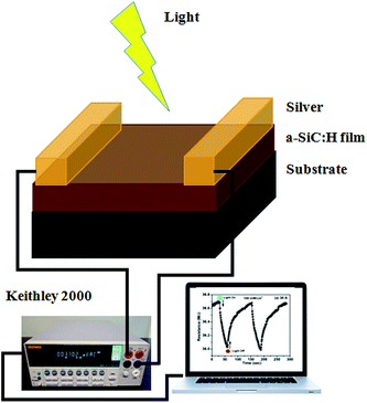
The thicknesses of the P-doped a-SiC:H film achieved were found to be in the range 120 ± 15 nm as measured by the Talystep (Rank Taylor and Hobson) thickness profiler. The deposition rate of P doped a-SiC:H films achieved were found to be 50–60 nm min−1. The XRD experiments of the films were carried out by Philips X'Pert PRO PANanalytical diffractometer using a CuKα (1.542 Å) X-ray source in the scanned region of 10–60°. A scanning step of 0.02° is used at a time of 1 s per step. The surface morphology of a-SiC:H thin films were analyzed by the SEM (Leo Electron Microscope – model no. LEO 440). The resolution of the SEM is 3 nm and the scanning measurement was performed at ∼10 kV voltages. A Renishaw In Via reflex micro-Raman spectrometer using a 514.5 nm Ar+ laser for excitation at a power of 15 mW has been used for studying the structural properties. Silver/P doped a-SiC:H/c-Si metal–insulator–semiconductor (MIS) device structure was fabricated on the highly doped silicon wafer with an area of ∼0.196 cm2. The SIMS analysis was performed using a 25 kV Bi+ TOF-SIMS (time-of-flight SIMS) system, ION-TOF with sputtering of 1 kV O2+ ions at a 45° incident angle. The beam currents were 1 pA and 30 nA for the analysis gun and the sputtering gun, respectively. The capacitance–voltage (C–V) measurements of MIS structure were carried out using Keithley 4200 semiconductor characterization systems. All the measurements were carried out at 1 MHz frequency. Silver as the top-electrode was thermally evaporated under a vacuum of ∼10−5 mbar onto the thin film through a shadow mask of 0.079 cm length and 0.5 cm width in a coplanar structure for the electrical and optical measurements. Optical transmittance measurements were performed using a Perkin Elmer spectrophotometer (Lambda 950) to calculate the absorption coefficient (α). The values of the optical band gap (Eg) of the P doped a-SiC:H films were evaluated using Tauc's formula, (αhυ)1/2 = B(hυ − Eg), where hυ is the photon energy, B is the edge width parameter related to the Urbach edge or disorder in the films. The value of Eg has been evaluated by extrapolating (αhυ)1/2 versus hυ curve to zero abscissa. Fig. 1 shows the schematic of the photo detection measurement setup. The photoconductive response of the films deposited on the glass substrate using coplanar structure was recorded by Keithley's digital multimeter (model-2000) automated in Labview software. The sample was kept 25 cm away from the lamp and no heating effect was observed. To further avoid the heating effect, the photo response of the films was recorded in the cyclic order of 30 s light on and 30 s off. The intensity of the incident light was controlled by controlling the applied voltage to the bulb and the intensity of the bulb is well calibrated with the different voltage signal.
 |
| | Fig. 1 Schematic of the photo detection measurement set up. | |
3. Results and discussion
3.1. XRD patterns
Fig. 2 shows the XRD patterns of P doped a-SiC:H films deposited at different arc currents ranging from 30 to 100 A at room temperature. In all the samples deposited at room temperature (RT), a broad diffraction peak is observed at 36–37°, which reveals that the deposited films are dominantly amorphous in nature. At arc current of 30 A, two separate broad peaks one at 25° and another at 36–37° indicate the different phases of amorphous carbon/silicon and silicon carbide, respectively. Sharp reflection observed at 33.4° is due to the crystalline phase of SiC at the interface of a-SiC:H thin film and the crystalline silicon wafer [JCPDS-892216].27 Small reflections other than 33.4° are due to the silicon substrate [JCPDS-772111].28 The crystallite size (d) from the sharp reflection at 33.4° due to the interface of a-SiC:H film and Si wafer is calculated from the well known Scherer formula expressed as:| |
 | (1) |
where λ is the wavelength of X-ray radiation, β is the full width at half maximum (FWHM) of XRD peak at diffraction angle θ. The crystallite size calculated from the Scherer formula is found to be about 30–32 nm. Inset of Fig. 2 shows the enlarged view of the XRD peak at ∼33.4° which corresponds to the crystalline phase of SiC in the a-SiC:H films grown at different arc currents. The maximum peak intensity accompanied with the broadened peak clearly manifests the preferable silicon carbide phase formation which in turn yields less micro-stress in the film grown at 60 A arc current, whereas, the peak shift in 30 and 100 A arc currents deposited films indicates the macro-strain generation. Therefore, one can elucidate that when the arc current was 30 A, the film growth appears to be a different amorphous phase of carbon/silicon and silicon carbide because of the low surface diffusion of the species (ions, atoms) on the substrate, but with the increase of arc current during the growth of the film, the species find the energetically favorable sites for the nucleation of the interface of a-SiC films. Vacuum arc produces a high temperature at the cathode surface and the evaporation of source material into a form of the plasma plume. Then, the plasma plume expands in a vacuum and reaches a substrate surface to condense into thin films. The deposition process of FCVA consists of plasma generation, transformation, and condensation. Therefore, the arc current could greatly influence the properties of the deposited films.
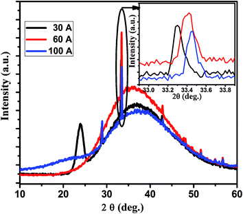 |
| | Fig. 2 Typical X-ray diffraction patterns of P doped a-SiC:H films deposited with different arc currents of 30, 60 and 100 A. | |
3.2. SEM and EDAX
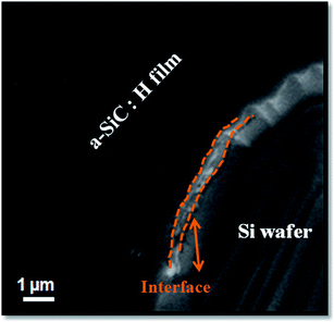
Fig. 3 shows a typical SEM image of P doped a-SiC:H film deposited at 60 A arc current of a patterned Si substrate in the vicinity of the a-SiC:H/c-Si interface. One can see that the surface of the film appears to be very smooth. Further, the SEM analysis on the cross section part revealed some crystallites phase decorating the interface between the a-SiC:H layers and Si substrate. The elemental concentrations of P doped a-SiC:H films deposited at different arc currents have been evaluated from the EDAX. The concentration of silicon and carbon evaluated from the spectra in the films deposited at 30 A arc current are found to be 88.27 at.% and 11.67 at.%, respectively. With the increase of arc current at 60 A, the carbon concentration in the P doped a-SiC:H film increased to 28.14 at.% and silicon concentration decreased to 71.76 at.%. At arc current of 100 A, the carbon content in the a-SiC:H films reduced to 21.19 at.% and silicon concentration increased to 78.61 at.%. The reason for the increase in the carbon concentration up to 60 A might be the optimum arc current on the silicon cathode during the arcing condition which is required to decompose C2H2 gas to get the maximum carbon content. At 100 A arc current there might be the depletion of the carbon source available from the C2H2 gas due to the higher ionization of the silicon cathode. The P contents evaluated in all the films are found to be <0.1 at.%. The higher intensity in the XRD pattern and the high carbon content in the EDAX result of 60 A arc current grown film elucidated that the high carbon content is preferred for the silicon carbide phase formation accompanied with the less stress generation in the film.
 |
| | Fig. 3 Typical SEM micrograph of P doped a-SiC:H film deposited with arc current 60 A. | |
3.3. Raman spectroscopy
The Raman spectra for the P doped a-SiC:H films deposited at different arc currents are shown in Fig. 4 for the wave number range from 150 to 1950 cm−1. Raman technique is a nondestructive important characterization tool for the silicon and their alloy films. Raman process is based on the inelastic scattering of photons by the phonons, when the energy of photon is greater than the band gap of the material. The mixing of C and Si leads to very complex structures with Si–Si, C–C and Si–C bonds. Such bonds are observed in the Raman spectra. The spectra exhibit three regions, which are assigned to Si–Si (250–600 cm−1), Si–C (650–1050 cm−1), and C–C (1100–1750 cm−1) vibrational mode.1 The wide band centered at around 480 cm−1 is due to the amorphous phase of Si–Si bonds. The downshift in Si–Si peak position and FWHM indicates the decrease in the structural angular distortion, which implies improved short range order in a-SiC:H films.29 Shi et al.16 reported that the increase in the silicon content shifts the Raman peak of the TO mode towards the lower wave number side. In the present case, TO mode appears at 482.5, 470.5 and 473.1 cm−1 in the films deposited at 30, 60 and 100 A arc currents, respectively. But in our case, the silicon content and the TO mode shift show a linear relation. In addition, the Raman spectra showed a broad weak band in the range of 600–1050 cm−1 that is due to the superposition of various peaks like 660, 760, 780, 950 and 960 cm−1 corresponding to SiH (wagging/bending),30 amorphous SiC,31 TO and LO modes of 3C–SiC30 and second order of Si–Si,32 respectively. It is important to notice that the Raman spectra showed a band centered at ∼775 cm−1, in a-SiC:H films deposited at different arc currents which is attributed to the presence of Si–C bond, whereas, in the previous report of Choi et al.33 this band was not detected in their Raman spectra. The greater intensity of the C–C bonds in the Raman spectra of P doped a-SiC:H films deposited at 30 A arc current exhibits the more graphitic carbon content which coexists with the silicon carbide phase. Further, the band at 1200–1700 cm−1 (C–C bonds) is more broader accompanied with the less intensity in a-SiC:H films deposited at 60 and 100 A arc current which clearly indicates that the films are having a large amount of the disordered phase of carbon.
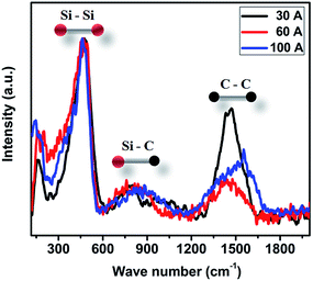 |
| | Fig. 4 Typical Raman spectra of P doped a-SiC:H films deposited with different arc currents of 30, 60, 100 A. | |
3.4. SIMS analysis
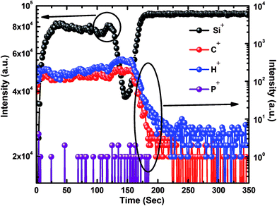
Fig. 5 shows the ToF-SIMS depth profiles of the selected positive secondary ions of P doped a-SiC:H film deposited at 60 A arc current. ToF-SIMS is a high resolution destructive technique and provides the elemental information even from the depth of the material. The detection limit for P concentration in a-SiC:H films is found to be 5 × 1015 cm−3 which might be attained by limiting the residual gas re-adsorption during the measurement. The atomic percentage of P atoms were calculated and found to be as <0.1 at.%. From the ToF-SIMS depth profile, it is clearly confirmed that the species C, H, P and Si constitute the a-SiC:H film. Ion implantation theory suggests that the heavier ions lose their energy near the surface of the substrate and they diffuse just near the substrate surface. In contrast, the lighter ions diffuse deeper into the substrate. From the depth profile, one can clearly see that the lighter hydrogen ions diffuse deeper into the substrate than the carbon ions. The SIMS spectra reveal that C and H concentration sharply decrease, whereas, the Si concentration increases at the interface of a-SiC:H film and c-Si substrate. It can be clearly comprehended from the SIMS spectra of the P doped a-SiC:H film that after a definite sputtering time the concentration of silicon decreases as compared to carbon and hydrogen, which is a clear evidence of sputtering of element from the interface of the film where silicon and carbon exist in their nanocrystalline form.
 |
| | Fig. 5 Typical SIMS data of P doped a-SiC:H film deposited with arc current of 60 A. | |
3.5. Electrical and optical properties of films
Fig. 6(a) shows the variation of dark conductivity (σD) versus inverse of temperature for P doped a-SiC:H films, deposited at different arc currents. It is evident from the figure that the variation of σD is a thermally activated process that follows a relation of the form:| |
σD = σ0![[thin space (1/6-em)]](https://www.rsc.org/images/entities/char_2009.gif) exp(−ΔE/kT) exp(−ΔE/kT)
| (2) |
where σ0 is the conductivity pre-exponential factor, ΔE is the activation energy and k is the Boltzmann constant and T is temperature in Kelvin. The variations of σD, ΔE and Eg evaluated for P doped a-SiC:H versus arc current are shown in Fig. 6(b)–(d), respectively. It is evident from Fig. 6(b) that the values of σD increase from 2.7 × 10⁻⁴ to 0.89 ohm−1 cm−1 and those of ΔE decrease from 0.21 to 0.08 eV (Fig. 6(c)) with the increase of arc current from 30 to 100 A. The value of Eg in P doped a-SiC:H film deposited at 30 A arc current is found to be 2.2 eV which increases to 2.4 eV in the film deposited at 60 A arc current and it becomes 1.9 eV in the film deposited at 100 A arc current (Fig. 6(d)). The values of σD and ΔE of P doped a-SiC:H films obtained in the present study using FCVA technique are found to be consistent or better than the values of σD (10−7 to 101 ohm−1 cm−1), ΔE (0.35–0.1 eV) and Eg (1.9–2.2 eV) of a-SiC:H films deposited by PECVD34,35 and ECR-CVD14 techniques. The increase of σD is accompanied with the decrease of ΔE with the increase of arc current used in the deposition of P doped a-SiC:H films. This indicates that either efficient doping is taking place which gives rise to the shift of Fermi level towards the conduction band or the crystallinity in the film is increasing. In the present case, use of the high arc current increases the ionization process on the arc spot that increases the energy of atoms and ions ejected. Furthermore, these atoms and ions having high energy increase the rate of ionization of C2H2 gas, which create a proper bond formation in the films and provides the extra charge carrier for the conduction. The increase of the Eg in P doped a-SiC:H film deposited at 60 A arc current is correlated with the increase of carbon concentration and decrease of the silicon concentration and beyond 60 A arc current the value of Eg decreases to 1.9 eV due to the reduction in the value of carbon content incorporated in the a-SiC:H film. This is corroborated with the EDAX results.
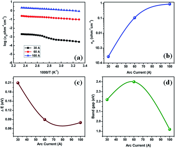 |
| | Fig. 6 (a) Variation of σD with the inverse of temperature for P doped a-SiC:H films deposited with different arc currents, (b) σD, (c) ΔE and (d) Eg versus the arc current for P doped a-SiC:H films. | |
FCVA is a well-established commercial technique for the deposition of metallic coatings and ta-C film/diamond-like carbon (DLC) thin films.36–39 It is a low voltage and high current (35V–50 V, 100 A) process. The cathodic vacuum arc is generally produced from the cold cathode whose material has to be deposited. The ions are ejected perpendicular to the cathode and macro particles are ejected at 10–20° to the cathode surface. The macro particles are removed by using the magnetic filter, pulsed technique of arcing and in the reactive mode of arcing.36–39 Ionized vapor of material created in the cathodic arc enhances the ability to independently control the ion flux and ion energy at the substrate. It also allows a better control of the ion bombardment of the growing film and better thickness homogeneity by applying external bias and temperature. The energy of the ionized particle is between 10 to 60 eV depending upon the depositing material which can be further enhanced by applying the negative bias to the substrate. The material flux emitted by the explosion or by the evaporation is composed of ions, neutral atoms, electrons and micro droplets of the material to be deposited. The micro droplets are removed by guiding the material flux through a magnetic filter (magnetic solenoid)36,37 and using pulsed technique.38,39
This deposition technique has the advantages of high deposition rate, processing at room temperature and low cost where no hazardous gases like SiH4, PH3 and B2H6 are used to deposit doped silicon films. Therefore, the FCVA process for fabricating silicon thin films using solid silicon cathode as a source material may be preferred as an alternative method to the conventional PECVD technique. In the FCVA process, mainly silicon, carbon and their combinations of ions are responsible for the film growth, but in the PECVD technique precursor like SiH, SiH2, (SiH2)n, CH3, and CH2 etc. are the main source in the silicon or carbon plasma for the synthesis of silicon or silicon carbide films. In the presence of hydrogen source which is available from the C2H2 gas in the present study, silicon and carbon ions generated during the arc react with the active hydrogen ions, the FCVA process appears to be similar to the PECVD process in forming the SiHx and CHx precursors for the growth of a-SiC:H films. As compared to the PECVD technique, FCVA technique has the higher magnitude of the plasma density, which resulted in the higher thin film deposition rate. The growth of the intrinsic silicon films by this technique has to be attempted. It may be possible by increasing the temperature of the cathode material which will increase the conductivity of the intrinsic cathode material for the initiation of the arc and also by making the cathode of the mixture of the silicon and carbon powders in the desired percentage for the silicon carbide film formation.
3.6. I–V and C–V measurements of heterojunction
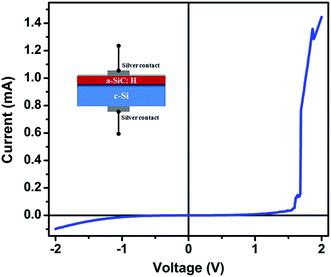
Fig. 7 shows the typical I–V curve of P doped a-SiC:H films deposited at 60 A arc current in the silver/P doped a-SIC:H/c-Si (MIS) structure. This non-linear increase in the current with the applied voltage gives the information about the conduction mechanism of P doped a-SiC:H films. The I–V curve of the silver/P doped a-SiC:H films/c-Si heterojunction was recorded at room temperature and it indicates that the MIS structure behaves as a Schottky junction,40 which is described below by the equation:| | |
I = Is[exp(eV/nkBT)−1],
| (3) |
where| |
Is = A*T2![[thin space (1/6-em)]](https://www.rsc.org/images/entities/char_2009.gif) exp(−eΦb/kBT), exp(−eΦb/kBT),
| (4) |
where V is the applied voltage, e is the charge of the electron, n is the diode ideality factor, T is the temperature in Kelvin, kB is the Boltzmann constant, A* is the effective Richardson constant, Φb is effective barrier height, and Is is the reverse saturation current. The value of reverse Is has been calculated by the interpolation of exponential slope of I at V = 0 and the value of diode ideality factor has been calculated using eqn (3). It is found that the values of Is and the diode ideality factor are 1.45 × 10⁻⁵ A and 1.5–1.7, respectively. Magafas et al.41 reported the optimized diode ideality factor of 1.02 of Al/a-SiC:H Schottky diode after thermal annealing the a-SiC:H thin films at 600 °C, whereas, the comparable diode ideality factor has been obtained without using any thermal annealing process in the present study. This infers that the P doped a-SiC:H films deposited by the FCVA process is a very interesting material for future potential applications.
 |
| | Fig. 7 Typical I–V curve of silver/P doped a-SiC:H/c-Si heterojunction diode. Inset shows the schematic of a heterojunction diode. | |
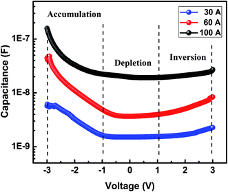
Fig. 8 shows the capacitance–voltage (C–V) characteristics of the silver/P doped a-SiC:H/c-Si (MIS) structure. The C–V measurement of the MIS structure is the same as metal oxide semiconductor (MOS) structure and the charges accumulated are the capacitance between the insulator and semiconductor. The a-SiC:H thin films contain defects which act as the trap centers capturing mobile carriers. There are variations in the C–V characteristics of a-SiC:H thin films deposited at different arc currents. In general, all the samples have three regions of operations:42 accumulation at negative bias, depletion at positive/negative bias and inversion at positive bias with the measured value of C corresponding either to the insulator capacitance (Cins) or to the series sum of the insulator capacitance and the capacitance of the amorphous semiconductor, respectively. The inversion is explained by the extraordinarily long generation times for the minority carriers and activated at much higher bias due to the presence of traps. Any devices made out of these thin films operate under non-equilibrium conditions. Under external excitations, they come back to the equilibrium condition through the carrier relaxation and recombination process. The existence of traps and defects affects the performance of any device. These trap levels capture carriers, which lie near the Fermi-level in the semiconductor.43 Spear et al.44 reported density of states (DOS) determination of a-Si:H film by the C–V relationship. This method was described by Schroder42 and used for a-Si:H MIS structure by Nandi et al.45 The behavior of the curve fits very well with the standard Mott–Schottky relationship for a simple Schottky barrier device.42
 |
| | Fig. 8 Typical C–V curves of silver/P doped a-SiC:H/c-Si heterojunction in P doped a-SiC:H films deposited with different arc currents. | |
The C–V measurements were carried out with the bottom electrode to the ground, and the top electrode voltage swept from +3 V to −3 V by 0.1 V step decreasing. The dielectric constant εs, calculated at the accumulation, is given by following relation42
where
C0 is the accumulation capacitance,
ε0 is the permittivity of the free space (8.854 × 10
−14 F cm
−1),
d is the film thickness, and
A is the area of the electrodes. The DOS was evaluated in the transition region between the accumulation and the depletion region given by the following relation
42| | |
d(1/C2)/dV = 2/(ε0εsqNAA2)
| (6) |
The value of DOS in P doped a-SiC:H film deposited at 30 A arc current is found to be 9.6 × 1016 cm−3 eV−1 which increases to 2.1 × 1017 cm−3 eV−1 in the film deposited at 60 A arc current and it becomes 4.8 × 1017 cm−3 eV−1 in the film deposited at 100 A arc current. The variation of DOS with the increase of arc current of P doped SiC:H film follows the same trend as that of the dark conductivity which might be a confirmation of the efficient doping in the P doped a-SiC:H films deposited at higher arc currents. Chew et al.46 while studying the density of states in undoped a-SiC:H films using a high frequency C–V technique reported the value of 3 × 1015 cm−3 eV−1. The density of states evaluated in the present study is found to be nearly two order higher than the density of states reported in undoped a-SiC:H films by Chew et al.46 which may be due to the phosphorous doping in the a-SiC:H films.
3.7. Photoconductive properties
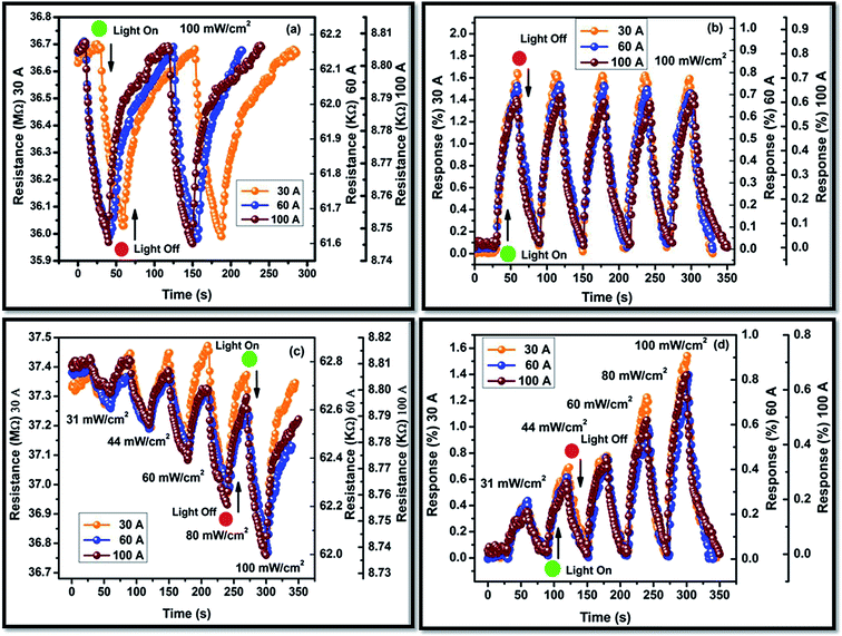
The P doped a-SiC:H films deposited at different arc currents have been investigated for their photoconductive response. The change in the electrical resistance of the films deposited at different arc currents have been recorded as a function of time in the dark as well as in the illumination of ∼100 mW cm−2 (Fig. 9(a)). The repeated cycles of illumination have been recorded with time to analyze the reproducibility of the results. It has been observed that the electrical resistance of the P doped a-SiC:H film decreases on the illumination and again recovered almost in the dark condition. The electrical resistance of the P doped a-SiC:H film deposited at 30 A arc current decreases from 36.6818 to 35.9902 MΩ (ΔR ≈ 691.6 kΩ) with 30 s at the illumination intensity of ∼100 mW cm−2. The decrease in the electrical resistance can be ascribed to the photo excited charge carriers. The change in the electrical resistance of the films can be given by47| |
 | (7) |
where, l, d and t are the length, width and thickness of the P doped a-SiC:H films, q and μ are the electronic charge and the mobility, Δn is the change in the concentration of charge carriers on the illumination. The dynamic resistance of the films can be described as:| |
 | (8) |
| |
 | (9) |
where, Rl and Rd are the dynamic resistances under the light (response) and dark (recovery), respectively, R0 is the steady state resistance, τres and τrec are the time constant of response and recovery, respectively. The dynamic resistance curves of both the samples have been fitted by the eqn (8) and (9) for the evaluation of the time constant of the response and the recovery. The time constant of the response (τres) has the values in the range of 7.8 to 9.5 s, whereas, the time constant of the recovery (τrec) has the values of 6.2 to 12.8 s for the P doped a-SiC:H films deposited at different arc currents. Moreover, the change in the electrical resistance of the P doped a-SiC:H films have been converted into the photo response by using the formula,| |
 | (10) |
 |
| | Fig. 9 The change in the resistance of the P doped a-SiC:H films deposited with different arc currents measured at (a) ∼100 mW cm−2 and (c) different intensities varying from 31 to 100 mW cm−2. Response of the P doped a-SiC:H films deposited with different arc currents at (b) ∼100 mW cm−2 and (d) different intensities varying from 31 to 100 mW cm−2. | |
The change in the electrical resistance in the P doped a-SiC:H film having a lower conductivity (at 30 A arc current) is larger than the P doped a-SiC:H film having a higher conductivity (at 100 A arc current). However, the P doped a-SiC:H film deposited at 30 A arc current has the higher photo response (∼1.6%) than that of the P doped a-SiC:H films deposited at 60 (∼0.75%) and 100 A arc current (∼0.65%) (Fig. 9(b)) at the illumination intensity of ∼100 mW cm−2. The photo response behavior of the P doped a-SiC:H films is comparable to the other semiconductor based photodetectors.48–51 Gowda et al.51 reported the enhanced photo response in a few layer graphene photo detector with the response and recovery time of 5 ± 2 s and 55 ± 3 s, respectively. The response time of 7.8 to 9.5 s is comparable and the recovery time of 6.2 to 12.8 s reported by us in the present study is found to be better than the recovery time reported by Gowda et al. The decrease in the electrical resistance is brought about by the injection of electron to the conduction band and the generation of more and more electron–hole-pairs with the passage of illumination time. On the illumination, photons are absorbed by the film and the bound electron–hole pairs get generated. The change in the electrical resistance of the P doped a-SiC:H film has also been measured at different intensities of illumination ranging from 31 to 100 mW cm−2 as shown in Fig. 9(c). It has been observed that the change in the electrical resistance increase with the increase in the illumination intensity for P doped a-SiC:H films deposited at different arc currents. The intensity dependent change in the electrical resistance has also been converted in the photo response as shown in Fig. 9(d). The photo response of the P doped a-SiC:H films has also been plotted as a function of different intensities. The intensity of light is changed by changing the applied voltage at the light source. The photo response of the deposited samples increases almost linearly with the illumination intensity. It has been observed that the risen time becomes shortened with the increase in the intensity of incident light. Out of which some electrons have sufficient energy to overcome the potential barrier, leaving behind the holes and creates a local electric field. When the P doped a-SiC:H films are kept in the dark, the energy bands of the materials adjust themselves w. r. t. the Fermi level and established an equilibrium state. However, this equilibrium state can be disturbed by the thermal excitation that makes some electrons and holes free and again a thermal equilibrium state is achieved by the material. On the application of the electric field, the bands are again disturbed and a net flow of charge takes place until a new equilibrium state is reached. This net flow of charge in the absence of the external illumination is responsible for the dark current, which depends on both the operating temperature as well as the applied electrical field.52,53 Since, the film surface also gets adsorbed with the oxygen molecules and adsorption of these foreign oxygen molecules creates electron trapping sites on the film surface. These electrons trapping sites capture the electrons and oxygen molecules turn into negative ions [O2(g) + e− → O2−(ad)] and contributes in the dark current. On the illumination of P doped a-SiC:H films, the electron–hole pairs [hυ → e− + h+] are generated and separated out for the conduction,54 which increases the electrical conductivity (decrease in the electrical resistance) for the films.
The increase in the electrical conductivity of the P doped a-SiC:H films can involve the following conduction mechanisms viz. the electronic transition, the excitons, the hopping or the tunneling and band to band transition. The electronic transition can be further divided into several processes such as absorption and excitation, recombination, trapping and capture. The absorption of light photons by the atoms of the films and their subsequent generation of electron–hole pairs is followed by the transitions from the valence band to the conduction band, the defect states to the conduction band and the valance band to the unoccupied energy levels. In the recombination process electrons are de-excited and return back to the original states. This process also involves the recombination of negatively charged oxygen and excess holes [h+ + O2−(ad) → O2(g)] pushed to the film surface by the local electric field. This process creates the deficiency of the hole and the recombination of unpaired electron becomes difficult and recombination only takes place after the adsorption of new oxygen molecules on the surface.54 This results in the slow recovery of the samples. Besides these processes, the charge carrier trapping and capture processes also affect the photoconduction behavior of the materials. These processes involve the transitions between the shallow levels and conduction band and the shallow levels and valance band, in the thermal equilibrium. The hole and electron traps coexist in the amorphous films, which are responsible for the longer response time of the photo detecting material. Thus, all these transitions are responsible for the response and recovery rate of the deposited films. The difference in the photo response of the deposited films may be caused by the conductivity and band gap. The presence of different DOS in a-SiC:H films also play an important role in the recombination process under illumination.
4. Conclusions
The phosphorus doped a-SiC:H thin films have been deposited at room temperature by the FCVA technique using different arc currents ranging from 30 to 100 A. The effect of arc currents on the structural, electrical and optical properties of P doped a-SiC:H films have been studied. The XRD patterns show that the grown films are dominantly amorphous in nature with the crystalline interface of SiC films. The crystallite size of the films grown was around 30–32 nm. Raman spectra also confirm the Si–C bond formation with Si–Si and C–C nucleation in films. The σD of P doped a-SiC:H film increase from 2.7 × 10⁻⁴ to 0.893 ohm−1 cm−1 and ΔE decrease from 0.21 to 0.08 eV on increasing the arc current from 30 to 100 A. The Eg of P doped a-SiC:H films were found to be in the range of 1.9 to 2.4 eV with the maximum 2.4 eV at 60 A arc current. The properties of FCVA deposited P doped a-SiC:H films at different arc currents are comparable to the PECVD and ECR-CVD grown films. The silver/a-SiC:H/c-Si MIS structure was fabricated and the P doped a-SiC:H/c-Si heterojunction diode showed the diode ideality factor between 1.5 to 1.7 and density of states lie between 9.6 × 10¹⁶ to 4.8 × 1017 cm−3 eV−1. The photo response behavior of the P doped a-SiC:H films depends on the arc current and the fast response and recovery time as 7.8 to 9.5 s and 6.2 to 12.8 s, respectively, recorded in the present study. On the basis of the present results, we infer that the films grown at 60 A arc current are very useful for the device application. These films can be used in the top layer of solar cell as a light dependent resistor which senses the intensity of light and the associated device make the street light ON and OFF. This type of coating material on the solar cells can provide the intelligent energy saving system for future generation.
Acknowledgements
The authors are grateful to Prof. R. C. Budhani, the Director, CSIR-National Physical Laboratory, New Delhi (India) for his kind permission to publish this paper. They wish to thank to Dr V. P. S. Awana for providing the XRD patterns, to Mr K. N. Sood for providing the SEM micrograph, to Dr Sushil Kumar, Mr C. M. S. Rauthan, Ms Kalpana Lodhi and Mr Atul Bisht for useful discussion and their help. Mr R. K. Tripathi and Mr A. K. Kesarwani are grateful to the Ministry of New and Renewable Energy (MNRE) and to the Council of Scientific and Industrial Research (CSIR), Government of India, respectively, for providing financial assistance during the course of this work.
References
- P. Melinon, B. Masenelli, F. Tournus and A. Perez, Nat. Mater., 2007, 6, 479 CrossRef CAS PubMed.
- R. Maboudian, C. Carraro, D. G. Senesky and C. S. Roper, J. Vac. Sci. Technol., A, 2013, 31, 050805 Search PubMed.
- S. H. Kim, D. J. You, J. H. Park, S. E. Lee, H. M. Lee and D. Kim, Appl. Phys. Lett., 2012, 101, 133910 CrossRef.
- P. K. Chang, P. T. Hsieh, C. H. Lu, C. H. Yeh and M. P. Houng, Sol. Energy Mater. Sol. Cells, 2011, 95, 2659 CrossRef CAS.
- M. V. Pelegrini, G. P. Rehder and I. Pereyra, Phys. Status Solidi C, 2010, 7, 786 CAS.
- W. Daves, A. Krauss, N. Behnel, V. Häublein, A. Bauer and L. Frey, Thin Solid Films, 2011, 519, 5892 CrossRef.
- L. Touahir, A. Cheriet, D. A. Dalla Corte, J. N. Chazalviel, C. H. de Villeneuve, F. Ozanam, I. Solomon, A. Keffous, N. Gabouze and M. Rosso, J. Power Sources, 2013, 240, 551 CrossRef CAS.
- C. Coletti, K. V. Emtsev, A. A. Zakharov, T. Ouisse, D. Chaussende and U. Starke, Appl. Phys. Lett., 2011, 99, 081904 CrossRef.
- F. Liu, A. Gutes, I. Laboriante, C. Carraro and R. Maboudian, Appl. Phys. Lett., 2011, 99, 112104 CrossRef.
- I. A. Yunaz, H. Nagashima, D. Hamashita, S. Miyajima and M. Konagai, Sol. Energy Mater. Sol. Cells, 2011, 95, 107 CrossRef CAS.
- P. C. Chen, J. Xu, H. Chen and C. Zhou, Nano Res., 2011, 4, 290 CrossRef CAS.
- S. Janz, S. Riepe, M. Hofmann, S. Reber and S. Glunz, Appl. Phys. Lett., 2006, 88, 133516 CrossRef.
- S. Zhang, L. Raniero, E. Fortunato, L. Pereira, N. Martins, P. Canhola, I. Ferreira, N. Nedev, H. Águas and R. Martins, J. Non-Cryst. Solids, 2004, 338–340, 530 CrossRef CAS.
- H. Shen, T. Wu, Y. Pan, L. Zhang, B. Cheng and Z. Yue, Thin Solid Films, 2012, 522, 36 CrossRef CAS.
- S. F. Yoon, R. Ji and J. Ahn, Mater. Chem. Phys., 1997, 49, 234 CrossRef CAS.
- M. M. M. Bilek and W. I. Milne, Thin Solid Films, 1996, 290–291, 299 CrossRef CAS.
- J. Han, M. Tan, J. Zhu, S. Meng, B. Wang, S. Mu and D. Cao, Appl. Phys. Lett., 2007, 90, 083508 CrossRef.
- Y. Zeng, N. Dai, Q. Cheng, J. Huang, X. Liang and W. Song, Mater. Sci. Semicond. Process., 2013, 16, 598 CrossRef CAS.
- J. R. Shi, X. Shi, Z. Sun, E. Liu, H. S. Yang, L. K. Cheah and X. Z. Jin, J. Phys.: Condens. Matter, 1999, 11, 5111 CrossRef CAS.
- C. Srisang, P. Asanithi, K. Siangchaew, A. Pokaipisit and P. Limsuwan, Appl. Surf. Sci., 2012, 258, 5605 CrossRef CAS.
- F. Demichelis, G. Crovini, F. Giorgis, C. F. Pirri and E. Tresso, Diamond Relat. Mater., 1995, 4, 473 CrossRef CAS.
- F. Giorgis, C. F. Pirri, E. Tresso and P. Rava, Philos. Mag. B, 1997, 75, 471 CrossRef CAS.
- O. S. Panwar, M. A. Khan, B. Bhattacharjee, A. K. Pal, B. S. Satyanarayana, P. N. Dixit, R. Bhattacharyya and M. Y. Khan, Thin Solid Films, 2006, 515, 1597 CrossRef CAS.
- O. S. Panwar, M. A. Khan, G. Bhagavanarayana, P. N. Dixit, S. Kumar and C. M. S. Rauthan, Indian J. Pure Appl. Phys., 2008, 46, 797 CAS.
- O. S. Panwar, M. A. Khan, M. Kumar, S. M. Shivaprasad, B. S. Satyanarayana, P. N. Dixit and R. Bhattachryya, Jpn. J. Appl. Phys., 2009, 48, 065501 CrossRef.
- O. S. Panwar, M. A. Khan, B. S. Satyanarayana, S. Kumar and Ishpal, Appl. Surf. Sci., 2010, 256, 4383 CrossRef CAS.
- Standard Data, JCPDS-892216.
- Standard Data, JCPDS-772111.
- M. Daouahi and N. Rekik, J. Phys. Chem. C, 2012, 116, 21018 CAS.
- F. S. Tehrani, M. R. Badaruddin, R. G. Rahbari, M. R. Muhamad and S. A. Rahman, Vacuum, 2012, 86, 1150 CrossRef.
- T. Chen, Y. Huang, H. Wang, D. Yang, A. Dasgupta, R. Carius and F. Finger, Thin Solid Films, 2009, 517, 3513 CrossRef CAS.
- M. Künle, T. Kaltenbach, P. Löper, A. Hartel, S. Janz, O. Eibl and K. G. Nickel, Thin Solid Films, 2010, 519, 151 CrossRef.
- W. K. Choi, F. L. Loo, C. H. Ling, F. C. Loh and K. L. Tan, J. Appl. Phys., 1995, 78, 7289 CrossRef CAS.
- T. Mueller, W. Duengen, Y. Ma, R. Job, M. Scherff and W. R. Fahrner, J. Appl. Phys., 2007, 102, 074505 CrossRef.
- F. Demichelis, C. F. Pirri and E. Tresso, J. Appl. Phys., 1992, 72, 1327 CrossRef CAS.
- J. Robertson, Mater. Sci. Eng. R Rep., 2002, 37, 129 CrossRef.
- R. L. Boxman, S. Goldsmith, A. B. Shalom, L. Kaplan, D. Arbilly, E. Gidalevich, V. Zhitomirsky, A. Ishaya, M. Keidar and I. I. Beilis, IEEE Trans. Plasma Sci., 1995, 23, 939 CrossRef CAS.
- O. S. Panwar, Y. Aparna, S. M. Shivaprasad, M. A. Khan, B. S. Satyanarayana and R. Bhattacharyya, Appl. Surf. Sci., 2004, 221, 392 CrossRef CAS.
- O. S. Panwar, B. Deb, B. S. Satyanarayana, M. A. Khan, R. Bhattacharyya and A. K. Pal, Thin Solid Films, 2005, 472, 180 CrossRef CAS.
- S. Kumar, N. Dwivedi, C. M. S. Rauthan and O. S. Panwar, Vacuum, 2010, 84, 882 CrossRef CAS.
- L. Magafas, J. Kalomiros, D. Bandekas and G. Tsirigotis, Microelectron. J., 2006, 37, 1352 CrossRef CAS.
- D. K. Schroder, Semiconductor Material and Device Characterization, John Wiley & Sons Inc., New Jersey, 2006 Search PubMed.
- A. M. Goodman, J. Appl. Phys., 1963, 34, 329 CrossRef CAS.
- W. E. Spear, P. G. Le Comber and A. J. Snell, Philos. Mag. B, 1978, 38, 303 CAS.
- K. C. Nandi, A. K. Biswas and H. N. Acharya, Mater. Lett., 1991, 12, 171 CrossRef CAS.
- K. Chew, Rusli, M. B. Lu, S. F. Yoon, V. Ligatchev and J. Ahn, Diamond Relat. Mater., 2001, 10, 1273 CrossRef CAS.
- N. Kurra, V. S. Bhadram, C. Narayana and G. U. Kulkarni, Nanoscale, 2013, 5, 381 RSC.
- C. J. Docherty, C.-T. Lin, H. J. Joyce, R. J. Nicholas, L. M. Herz, L.-J. Li and M. B. Johnston, Nat. Commun., 2012, 3, 1228 CrossRef PubMed.
- R. H. Bube, Photoconductivity of Solids, John Wiley and Sons, New York, 1967 Search PubMed.
- L. Sang, M. Liao and M. Sumiya, Sensors, 2013, 13, 10482 CrossRef CAS PubMed.
- P. Gowda, T. Sakorikar, S. K. Reddy, D. B. Ferry and A. Misra, ACS Appl. Mater. Interfaces, 2014, 6, 7485 CAS.
- A. G. Chynoweth and W. G. Schneider, J. Chem. Phys., 1954, 22, 1021 CrossRef CAS.
- Y. Matsuoka, A. Fujiwara, N. Ogawa, K. Miyano, H. Kataura, Y. Maniwa, S. Suzuki and Y. Achiba, Sci. Technol. Adv. Mater., 2003, 4, 47 CrossRef CAS.
- R. S. Chen, C. A. Chen, H. Y. Tsai, W. C. Wang and Y. S. Huang, J. Phys. Chem. C, 2012, 116, 4267 CAS.
|
| This journal is © The Royal Society of Chemistry 2014 |
Click here to see how this site uses Cookies. View our privacy policy here. 


![[thin space (1/6-em)]](https://www.rsc.org/images/entities/char_2009.gif) exp(−ΔE/kT)
exp(−ΔE/kT)

![[thin space (1/6-em)]](https://www.rsc.org/images/entities/char_2009.gif) exp(−eΦb/kBT),
exp(−eΦb/kBT),
