Ab initio calculations of quantum transport of Au–GaN–Au nanoscale junctions
Tian Zhanga,
Yan Cheng*a and
Xiang-Rong Chen*ab
aInstitute of Atomic and Molecular Physics, College of Physical Science and Technology, Sichuan University, Chengdu 610065, China. E-mail: ycheng@scu.edu.cn; xrchen@scu.edu.cn
bInternational Centre for Materials Physics, Chinese Academy of Sciences, Shenyang 110016, China
First published on 9th October 2014
Abstract
We investigate the contact geometry and electronic transport properties of a GaN pair sandwiched between Au electrodes by performing density functional theory plus the non-equilibrium Green's function method. The Au–GaN–Au junction breaking process is simulated. We calculate the corresponding cohesion energy and obtain the equilibrium conductance and the projected density of states of junctions. We also calculate the pulling force of the four configurations, and the spatial electron density difference after the junction is broken. In addition, the current of junctions is computed under small bias. It is found that all junctions have large conductance showing a non-linear I–V relationship.
1. Introduction
Molecular electronics1,2 has become a hot topic in physics and materials science in the last decade. To develop molecular electronics, it is essential to understand quantitatively the electronic transport of molecular junctions between two metallic electrodes. When the molecule is attached to metallic electrodes, the electronic current will turn more complex. However, with the development of micro-fabrications and self-assembly techniques, it has become a reality for designing a molecule device or controlling the electronic transport properties on a nanoscale system.3The electronic transports through single-atomic contacts4 and molecules5 are of great fundamental interest since they might be applicable in future electronic and energy-conversion devices based on electron transfer, shot noise, heat transport, negative differential resistance, gate controlled, and so on. By trapping a single molecule in break junctions (MCBJ) formed by mechanical strain,6 electromigration7 and scanning tunneling microscopes (STM),8 the current–voltage (I–V) characteristic of single molecules has been extensively investigated. Remarkable progress in the experimental growth, control, and characterization techniques at the nanoscale has allowed producing many potentially useful molecular electronic devices, such as molecular wires, resonant tunneling diodes, molecular switches, molecular rectifiers, and molecular storage devices.9–22 Certainly, the theories also play a fundamental role in explaining these experiments and designing new ones.23,24
Recently, there is a strong motivation for examining the transport properties of Group III nitride based nanowires for possible applications in low-power and high-density field-effect transistors (FETs), solar cells, terahertz emitters, and detectors.25,26 Their outstanding physical and chemical stability enables the III-N devices to be operated under extreme environmental conditions. Huang et al.25 reported successfully the fabrication of logic gates and demonstrated the computation capabilities from assembled nanowire p-Si and n-GaN crossed nanowire junctions. Later, Renard et al.26 showed that the polar GaN/AlN axial heterostructures in nanowires grown by plasma-assisted molecular-beam epitaxy were subject to a clear quantum-confined Stark effect. They addressed the transport properties of the n-type GaN/AlN double-barrier nanowires.
In this work, we will focus on the effects of molecular contact geometry on the conductance and the I–V characteristics of the GaN molecule sandwiched between Au electrodes. We simulate the Au–GaN–Au junctions breaking process in the four different anchoring geometries, and calculate the I–V characteristics of the junctions at the equilibrium positions. The rest of the paper is organized as follows. The theoretical methods and the computational details are given in Section 2. Some results and discussion are presented in Section 3. Finally, the Summary of our main results are given in Section 4.
2. Theoretical method and calculation details
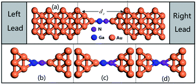
Our theoretical investigations for the electronic structure properties are based on the ab initio density functional theory (DFT) as implemented in the Siesta code.27 This method employs a linear combination of pseudo-atomic orbitals for the basis set and replaces the atomic cores by nonlocal norm-conserving Troullier–Martins pseudo-potentials,28 factorized in the Kleinman–Bylander form.29 In our calculations, we use the Perdew–Zunger form30 of the local-density approximation (LDA) to the exchange-correlation functional. Nonlocal scalar-relativistic Troullier–Martins pseudo-potentials are generated from the configurations: Au (5d106s1), Ga (4s24p1), and N (2s22p3). A single-zeta is used as the basis set for Au, and a double-zeta basis is adopted for the orbitals of the other species (Ga and N).The transport calculations have been performed with the ab initio transport code Smeagol,31–33 which is used to calculate the density matrix and the transmission coefficients of a two probe device using the non-equilibrium Green function (NEGF) formalism. The physical model is divided into three parts, namely left and right semi-infinite Au (1 0 0) metal electrodes and the central region. The latter contains the GaN molecule plus parts of the Au electrodes accommodating the molecule–surface interaction (see Fig. 1). The two semi-infinite leads are assumed to be in equilibrium with well-defined chemical potentials and act as current–voltage probes. Notice that the left and the right electrodes are considered perfect crystal and the chemical potential is well approximated by that of a perfect bulk electrode. In contrast, the electronic potential of the scattering region is calculated self-consistently for each applied bias.34–36 For this purpose we define the Green's function of the scattering region in the presence of the leads as:
 | (1) |
![[capital Sigma, Greek, circumflex]](https://www.rsc.org/images/entities/i_char_e139.gif) L and
L and ![[capital Sigma, Greek, circumflex]](https://www.rsc.org/images/entities/i_char_e139.gif) R are the self-energies, respectively, for the left and right lead. This allows us to evaluate the density matrix
R are the self-energies, respectively, for the left and right lead. This allows us to evaluate the density matrix
 | (2) |
![[capital Gamma, Greek, circumflex]](https://www.rsc.org/images/entities/i_char_e132.gif) α = i[
α = i[![[capital Sigma, Greek, circumflex]](https://www.rsc.org/images/entities/i_char_e139.gif) α −
α − ![[capital Sigma, Greek, circumflex]](https://www.rsc.org/images/entities/i_char_e139.gif) α+]. Since the DFT Hamiltonian HS depends solely on the density matrix, eqn (1) and (2) can be iterated until reaching self-consistency.
α+]. Since the DFT Hamiltonian HS depends solely on the density matrix, eqn (1) and (2) can be iterated until reaching self-consistency.
In what follows, the leads have an fcc crystalline structure and are oriented along the (1 0 0) direction. The unit cell of the extended molecule comprises a GaN molecule and 13 Au atomic layers each containing 3 × 3 atoms in the surface plane. A periodic boundary condition is applied in the basal plane (orthogonal to the transport direction) with four irreducible k-points in the two-dimensional Brillouin zone. The Brillouin zone is set to be 2 × 2 × 100 points following the Monkhorst–Pack k-point scheme.37 The cut-off energy and iterated convergence criterion for total energy are set to 200 Rydberg and 10−4, respectively. Furthermore, the charge density is integrated over 50 energy points along the semi-circle and 20 energy points along the line in the complex plane, and 20 poles are used for the Fermi distribution.
3. Results and discussion
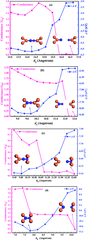
To gain insight into the possible structures of Au–GaN–Au junctions, we have made successive relaxations for each system by keeping all Au atoms in the leads fixed and only relaxing the apexes of the point contact in the center until the force on each atom is smaller than 0.1 eV Å−1 in each optimization process.38 The ground state energy is calculated as a function of the distance dz between the outer surface layers (not relaxation) (Fig. 1), thereby simulating the contact formation in a mechanically controlled break junction (MCBJ) experiment. We increase/decrease all atomic distances between them proportionally to change the distance dz between the two Au (1 0 0) surface, and subsequently the system is relaxed to form the equilibrium structure. In the following, we concentrate on four different structures for the gold contacts as shown in Fig. 1(a) GaN connected to pyramidal-shaped electrodes at the top site with the molecular axis parallel to the transport direction(z-axis), (b) GaN connected to the pyramidal-shaped electrodes at the hollow site to the left and at the top site to the right (molecular axis parallel to z-axis), (c) GaN connected to the pyramidal-shaped electrodes at the top site to the left and at the hollow site to the right (molecular axis parallel to z-axis), and (d) GaN connected to two hollow sites with the molecular axis parallel to z.The calculated conductance as a function of distance dz is shown in Fig. 2. This conductance G associated to the two-probe device can be calculated by using Fisher–Lee's relation39
 | (3) |
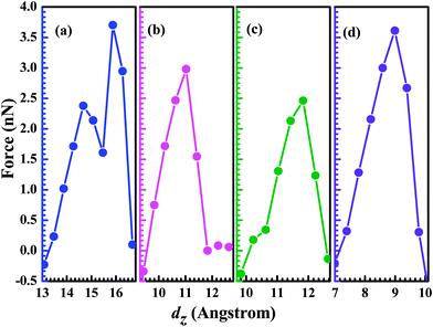
As the two contact distance is pulled apart, the interaction force between atoms also shows the corresponding change. In Fig. 3, we present the pulling force as a function of the electrodes' separation, which is calculated as Fz = dEtotal/dΔL, where Etotal (Au electrodes + GaN molecule) is the total energy of the system at each stretch and ΔL stands for the elongation of the system. In fact, the pulling force as a function of dz is characterized by elastics stages (where the force increases) followed by stress release. The existence of negative force means that the system is under compressive strain. For the configuration (a) the Ga–N bond is compressed at a small dz (<13.5 Å), and the Ga–N bond-length gets stretched as the distance dz is beyond 13.5 Å. Its maximum achieved force is calculated to be 3.70 nN, implying that Ga–N bond can't be stretched further when dz is larger than 15.872 Å. This is consistent with the obtained result by analyzing the calculated conductance as a function of dz. For the configurations (b), (c), and (d), the maximum achieved force is 2.98 nN at 11.031 Å (Au–N), 2.46 nN at 11.832 Å (Ga–Au), and 3.61 nN at 8.991 Å (Ga–N), respectively. The calculated results show that the strength of Ga–N bond is stronger than other bonds including the Ga–Au, and N–Au bonds. Although we find that out of four studied structures two structures break exactly at the Ga–N bond, the phenomenon can be put down to the reason that the Au atom and the N atom (Ga atom) have the different coordination numbers in the structure (a) and (d). In the structure (b), the Ga atom and Au atom have the same coordination number of 5, that is to say, the Ga atom and the Au atom lie on the same statue. The broken bond is the weak bond (N–Au) as the two contact distance is pulled apart continuously, which is similar to the structure (c) whose broken bond is the weak (Ga–Au) bond. However, in the structure (a) whose Au atom has the higher coordination number when compared to the Ga (N) atom, the broken bond is the Ga–N bond rather than the weak bond. The coordination atoms around the Au atom have the weak interaction with the N (Ga) atom, and in consideration of the tiny difference of the strength between the Au–N (Ga) bond and N–Ga bond, the superposition of the weak interaction and the strength of Au–N (Ga) bond can exceed the strength of the N–Ga bond. Hence, for the structure (a) and (d), the broken bond is the N–Ga bond.
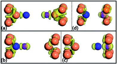
Additionally, we also calculate the spatial electron density difference when the pulling force is beyond the corresponding maximum achieved force (structural break) for the four configurations, which is illustrated in Fig. 4. The electron density difference, ρ′(r) = ρ(r) − ρatoms(r), between the self-consistently calculated electron density of the junctions after structural break, ρ(r), and that of free atoms placed at the same positions, ρatoms(r), describes how uneven the distribution of valence electrons of the junctions is after structural break. For the configuration (a), the electrons are distributed uniformly between the Au atom and Ga atom, Ga atom and N atom, and N atom and Au atom, meaning that they form the strong covalent bonding with the nearest-neighboring atoms. Such behavior is similar to that of the configuration (d). By observing the charge densities of the configurations (b) and (c), it can be found that the charge is more localized on the Ga–N atom rather than the right/left Au atom, which may be put down to the reason that Ga and N atoms have a stronger electronegativity.
To calculate the most stable structures for the four different configurations in different distances, we calculate the cohesion energy as a function of dz during the simulation process. The cohesion energy is defined as follows: E = E (Au electrodes + GaN molecule) − E (GaN molecule) − E (Au electrodes). The results of the calculation are shown in Fig. 2. It is found that there is a similar parabola in the curve of the total energy as a function of the distance dz for the four configurations. The minimum energy in every curve is located at the equilibrium distances. If the electrodes are free to relax, the system will naturally form the equilibrium structure with the equilibrium distance dz,eq corresponding to those energy minima. It can be found that, for the four different structures (a), (b), (c) and (d), its equilibrium distance is dz,eq = 14.272 Å, 11.031 Å, 9.832 Å and 7.791 Å, respectively. When the junctions are located at the optimal equilibrium positions, the Ga–N bond-length, dGa–N, is 1.873 Å for configuration (a), 1.900 Å for configuration (b), 1.951 Å for configuration (c) and 2.011 Å for configuration (d). The calculated results of Ga–N bond-length are also consistent with the calculated result (1.87 Å) of Song et al.42 In short, it is not difficult to find that the cohesion energy of the two probe systems at the optimal position is different in these four configurations. From the calculated results, it is also easy to see that the cohesion energy of the system increases in turn from configuration (a) to (d), and the equilibrium conductance of GaN in these four configurations at the optimal position is 1.50G0 for configuration (a), 1.75G0 for configuration (b), 0.61G0 for configuration (c), and 1.54G0 for configuration (d). In fact, the conductance values are the direct consequence of the small energy difference between the electrodes' Fermi energy EF and the molecular orbital which dominates HOMO or LUMO. The Kohn–Sham orbitals are mathematical objects rather than true molecular orbitals, hence their energy should be shifted43 which leads to the result that the calculated value of conductance may be larger than the experimental value. There are some studies on single-molecule junctions in a solvent that consider the energy offset of the dominant molecular orbital relative to the electrode Fermi level, which get very meaningful results.44,45 Unfortunately, there is no experimental value of conductance of the GaN molecule to compare with. But we expect that our theoretical prediction might be useful in further experiments and theories.
To further understand the conductance of Au–GaN–Au junctions, we can analyze the transmission spectrum T(E, V = 0) (Fig. 5) and the projected density of states (PDOS) (Fig. 6) of the GaN molecule. For the configuration (a), EF of Au is located at a peak in the transmission function. Thus, T(EF; 0) is dominated by a resonance corresponding to the energy of the highest occupied molecular orbital (HOMO), εHOMO. This provides a large conductance, so the Au–GaN–Au junctions have a large transmission. Such a transport channel is almost formed by px and py orbital electrons of Ga and N atoms, with an almost negligible contribution from their pz. For the configuration (b), the Ga atom on the side binds at the hollow site of the Au (1 0 0) surface, and for (c), the N atom on the side binds at the hollow site. Both their electronic coupling are considerably stronger than that in configuration (a), which leads to a strong broadening and shift of the resonances. The transmission becomes flat around the Fermi level. But it is not difficult to find that the configuration (c) have a stronger electronic coupling than (b) by observing the broadening degree of HOMO in the transmission spectrum. The Fermi level is located just above the HOMO for (b), with a stronger resonant effect in the transmission spectrum. Hence the HOMO contributes much to G so that (b) has the largest transmission among all the junctions. Its transport channel is mainly formed by the px and py orbits of the Ga and N atoms, a little pz of the N atom, and s orbital electrons of the Ga atom. For (c), the stronger electronic coupling induces the HOMO of GaN to broaden to a point where it becomes indistinguishable in the PDOS. As a consequence, there is no resonance at EF, but instead, T(E) is flat and featureless. This phenomenon is more obvious for configuration (d) due to the reason that (d) has the strongest electronic coupling.
The current is self-consistently calculated within the non-equilibrium Green's function approach with the voltage-dependent Landauer formula36
 | (4) |
| f(E − μL,R) = 1/{exp[(E − μL,R)/kBT] + 1}, | (5) |
To achieve a qualitative understanding of the underling physics, it is useful to calculate the transmission coefficients as a function of the energy for different biases and configurations, because the current through the system is proportional to the integral of the transmission coefficients in the energy window (EF − eV/2, EF + eV/2). The calculated transmission spectrum of T(E) is shown in Fig. 5, under the bias of 0 V, 0.4 V, 0.8 V, 1.2 V. For the configuration (a), we can observe a significant drift of the HOMO resonance to lower energies as the bias increases. Such a drift of the HOMO makes the HOMO away from the Au Fermi level. Because the transmission peak does not leave the energy window, the current and conductance remains relatively large. In contrast to the configuration (b), little change happens to the transmission coefficient around the Fermi level as the bias increases. For the remaining configurations (c) and (d), we can find the similar phenomenon: with the increasing bias, the HOMO of GaN gradually broadens. As a consequence, there is no resonance at EF, but instead, T(E) becomes flat and featureless.
4. Conclusions
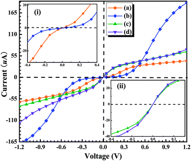
In summary, we have applied the density functional theory plus the non-equilibrium Green's function method to systematically investigate the transport properties of a GaN molecule sandwiched between two semi-infinite Au (1 0 0) metal electrodes in the four different anchoring configurations. We have simulated the Au–GaN–Au junctions breaking process and calculated the corresponding cohesion energy in the four different configurations. The obtained conductance of GaN in four configurations at the optimal position is 1.50G0, 1.75G0, 0.61G0 and 1.54G0, respectively. It can be found that the molecular-scale contact geometry plays a critical role in the absolute value of the conductance. By calculating the pulling force of the four configurations, and their spatial electron density differences after structural break, we can conclude that the Ga–N bond is stronger than other bonds including Au–Ga bond and Au–N bond. Additionally, we have also calculated the current of junctions at the optimal position under small bias for the four configurations. It is found that: for the configurations (a) and (b), the conductance (dI/dV) is smaller under the lower bias zone than that under the higher bias region, and for the configurations (c) and (d), the situation is reversed. Such behavior shows that the GaN junctions have the characteristic of the semiconductor-like junction.Acknowledgements
The authors would like to thank Dr S. Sanvito for his providing us the SMEAGOL code. We also thank the support by the National Natural Science Foundation of China under Grant nos 11174214 and 11204192 and the NSAF under Grant no. U1430117 and U1230201.References
- H. Song, M. A. Reed and T. Lee, Adv. Mater., 2011, 23, 1583 CrossRef CAS PubMed.
- C. Joachim, J. K. Gimzewski and A. Aviram, Nature, 2000, 408, 541 CrossRef CAS PubMed.
- D. R. Bowler, J. Phys.: Condens. Matter, 2004, 16, R721 CrossRef CAS.
- F. T. Liu, Y. Cheng, F. B. Yang and X. R. Chen, Chin. Phys. Lett., 2013, 30, 107303 CrossRef.
- P. Reddy, S. Y. Jang, R. A. Segalman and A. Majumdar, Science, 2007, 315, 1568 CrossRef CAS PubMed.
- M. A. Reed, C. Zhou, C. J. Muller, T. P. Burgin and J. M. Tour, Science, 1997, 278, 252 CrossRef CAS.
- H. Parket, Nature, 2000, 407, 57 CrossRef PubMed.
- B. Xu and N. J. J. Tao, Science, 2003, 301, 1221 CrossRef CAS PubMed.
- F. T. Liu, Y. Cheng, F. B. Yang and X. R. Chen, Phys. E, 2014, 56, 96 CrossRef CAS PubMed.
- J. X. Yu, Y. Cheng, S. Sanvito and X. R. Chen, Appl. Phys. Lett., 2012, 100, 103110 CrossRef PubMed.
- C. J. Xia, D. S. Liu, H. C. Liu and X. J. Zhai, Phys. E, 2011, 43, 1518 CrossRef CAS PubMed.
- M. Qiu and K. M. Liew, Phys. Lett. A, 2011, 375, 2234 CrossRef CAS PubMed.
- X. J. Liu and Z. An, Org. Electron., 2011, 12, 1352 CrossRef CAS PubMed.
- Y. P. An, C. L. Yang, M. S. Wang, X. G. Ma and D. H. Wang, Curr. Appl. Phys., 2010, 10, 260 CrossRef PubMed.
- G. B. Abadir, K. Walus and D. L. Pulfrey, J. Comput. Electron., 2009, 8, 1 CrossRef CAS PubMed.
- P. Zhao, P. J. Wang, Z. Zhang and D. S. Liu, Phys. B, 2010, 405, 446 CrossRef CAS PubMed.
- P. Zhao, P. J. Wang, Z. Zhang, M. J. Ren and D. S. Liu, Phys. B, 2010, 405, 2097 CrossRef CAS PubMed.
- P. Zhao, Z. Zhang, P. J. Wang and D. S. Liu, Phys. B, 2009, 404, 3462 CrossRef CAS PubMed.
- P. Zhao, P. J. Wang, Z. Zhang and D. S. Liu, Phys. Lett. A, 2010, 374, 1167 CrossRef CAS PubMed.
- C. J. Xia, D. S. Liu, C. F. Fang and P. Zhao, Phys. E, 2010, 42, 1763 CrossRef CAS PubMed.
- J. Huang, Q. Li, H. Su and J. Yang, Chem. Phys. Lett., 2009, 479, 120 CrossRef CAS PubMed.
- E. Zahedi and A. Pangh, Superlattices Microstruct., 2011, 50, 386 CrossRef CAS PubMed.
- V. M. García-Suárez, A. R. Rocha, S. W. Bailey, C. J. Lambert, S. Sanvito and J. Ferrer, Phys. Rev. B: Condens. Matter Mater. Phys., 2005, 72, 045437 CrossRef.
- K. H. Khoo, J. B. Neaton, H. J. Choi and S. G. Louie, Phys. Rev. B: Condens. Matter Mater. Phys., 2008, 77, 115326 CrossRef.
- Y. Huang, X. Duan, Y. Cui, L. J. Lauhon, K. H. Kim and C. M. Lieber, Science, 2001, 294, 1313 CrossRef CAS PubMed.
- J. Renard, R. Songmuang, G. Tourbot, C. Bougerol, B. Daudin and B. Gayral, Phys. Rev. B: Condens. Matter Mater. Phys., 2009, 80, 121305 CrossRef.
- J. M. Soler, E. Artacho, J. D. Gale, A. García, J. Junquera, P. Ordejón and D. Sánchez-Portal, J. Phys.: Condens. Matter, 2002, 14, 2745 CrossRef CAS.
- N. Troullier and J. L. Martins, Phys. Rev. B: Condens. Matter Mater. Phys., 1991, 43, 1993 CrossRef CAS.
- L. Kleinman and D. M. Bylander, Phys. Rev. Lett., 1982, 48, 1425 CrossRef CAS.
- J. P. Perdew, Phys. Rev. B: Condens. Matter Mater. Phys., 1986, 33, 8822 CrossRef.
- I. Rungger and S. Sanvito, Phys. Rev. B: Condens. Matter Mater. Phys., 2008, 78, 035407 CrossRef.
- A. R. Rocha, V. M. Garcia, S. W. Bailey, C. J. Lambert, J. Ferrer and S. Sanvito, Nat. Mater., 2005, 4, 335 CrossRef CAS PubMed.
- A. R. Rocha, V. M. Garcia-Suarez, S. Bailey, C. Lambert, J. Ferrer and S. Sanvito, Phys. Rev. B: Condens. Matter Mater. Phys., 2006, 73, 085414 CrossRef.
- C. Caroli, R. Combescot, D. Lederer, P. Nozieres and D. Saint-James, J. Phys. C: Solid State Phys., 1971, 4, 2598 CrossRef.
- L. V. Keldysh, J. Exp. Theor. Phys., 1965, 20, 1018 Search PubMed.
- S. Datta, Electronic Transport in Mesoscopic Systems, Cambridge University Press Cambridge, 1995 Search PubMed.
- H. J. Monkhorst and J. D. Pack, Phys. Rev. B: Condens. Matter Mater. Phys., 1976, 13, 5188 CrossRef.
- R. B. Pontes, A. R. Rocha, S. Sanvito, A. Fazzio and A. J. R. da Silva, ACS Nano, 2011, 5, 795 CrossRef CAS PubMed.
- D. S. Fisher and P. A. Lee, Phys. Rev. B: Condens. Matter Mater. Phys., 1981, 23, 6851 CrossRef CAS.
- M. Buttiker, Y. Imry, R. Landauer and S. Pinhas, Phys. Rev. B: Condens. Matter Mater. Phys., 1985, 31, 6207 CrossRef.
- I. S. Kristensen, D. J. Mowbray, K. S. Thygesen and K. W. Jacobsen, J. Phys.: Condens. Matter, 2008, 20, 374101 CrossRef CAS PubMed.
- B. Song, C. H. Yao and P. L. Cao, Phys. Rev. B: Condens. Matter Mater. Phys., 2006, 74, 035306 CrossRef.
- I. Baldea, Electrochem. Commun., 2013, 36, 19 CrossRef CAS PubMed.
- S. Y. Quek, H. J. Choi, S. G. Louie and J. B. Neaton, Nano Lett., 2009, 9, 3949 CrossRef CAS PubMed.
- I. Baldea, Nanoscale, 2013, 5, 9222 RSC.
| This journal is © The Royal Society of Chemistry 2014 |

