
The role of Schottky barrier in the resistive switching of SrTiO3: direct experimental evidence
Xue-Bing
Yin
,
Zheng-Hua
Tan
 and
Xin
Guo
*
and
Xin
Guo
*
Laboratory of Solid State Ionics, School of Materials Science and Engineering, Huazhong University of Science and Technology, Wuhan 430074, P. R. China. E-mail: xguo@hust.edu.cn
First published on 7th November 2014
Abstract
Single crystalline SrTiO3 doped with 0.1 wt% Nb was used as a model system to evaluate the role of the Schottky barrier in the resistive switching of perovskites. The Ti bottom electrode formed an ohmic contact in the Ni/Nb:SrTiO3/Ti stack, whereas the Ni top electrode created a strong Schottky barrier, which was reflected in a huge semi-circle in the impedance spectrum of the stack. Bipolar switching was achieved in the voltage range of −4 to 4 V for the stack, two clear resistance states were created by electric pulses, and the Schottky barrier heights corresponding to the high/low resistance states were experimentally determined. A direct relationship between the resistance state and the Schottky barrier height was thus established.
The phenomenon of resistive switching has been extensively observed in various perovskite oxides, such as Pr1−xCaMnO3,1 SrZrO3,2 SrTiO3,3 and BaTi0.95Co0.05O3,4 and Pb(Zr0.2Ti0.8)O3.5 Among perovskite oxides, SrTiO3 has been thoroughly investigated;6–12 the knowledge about SrTiO3 helps understanding the switching behaviours of other perovskite oxides. Therefore, SrTiO3 is addressed in this work as a model system.
Quite different mechanisms have been proposed to explain the switching behaviours of SrTiO3, and the most relevant switching mechanisms have been reviewed by Waser et al.13,14 and Sawa.15 Usually the work on acceptor-(e.g. Cr) doped SrTiO3 (ref. 6 and 9) emphasizes the property change in the crystal bulk, in which, oxygen vacancies (or oxygen ions) play a key role: either the fast transport of oxygen vacancies along dislocations10 or the formation of an oxygen-vacancy array under high electrical stress11 was suggested to be responsible for the switching. Guo16 performed the electroforming of acceptor-doped SrTiO3 single crystals at 200 °C and realized bipolar switching at room temperature. Since oxygen vacancies (or oxygen ions) are sufficiently mobile at 200 °C, this work established a clear relationship between the migration of oxygen vacancies and the resistive switching. In a very recent work,17 the concentration variation of oxygen ions at different resistance states was directly measured.
A Schottky barrier is formed at the metallic electrode/SrTiO3 contact, therefore, for donor-(e.g. Nb) doped SrTiO3 the role of the Schottky barrier is emphasized:7,8,14,15 the change in the Schottky barrier height under voltages of different polarities is responsible for the different resistance states. The important experimental results for the Schottky barrier model are:15 (1) the on/off resistance of Nb-doped SrTiO3 is inversely proportional to the electrode/SrTiO3 interface area, suggesting that the resistive switching takes place over the entire interface area, and (2) Nb-doped SrTiO3 with ohmic contact does not show any switching behaviour, whereas Nb-doped SrTiO3 with Schottky-type contact shows resistive switching, and the switching behaviour can be alternated by modifying the electrode/SrTiO3 interface.
However, the effect of the Schottky barrier was not separated from that of the bulk of donor-doped SrTiO3 in many cases. For example, the stack (interface plus bulk) capacitance was measured without differentiating the contribution of the crystal bulk from that of the interface;18 as a result, one could not conclude that the different capacitances in the low and high resistance states were only due to the interface effect. Also the direct link between the Schottky barrier height and the resistance state is still lacking.
An obvious advantage of the impedance spectroscopy technique is that the interface effect and the bulk contribution can be readily separated.19 Impedance spectroscopy has been popularly used to investigate the switching of Fe-doped SrTiO3,19 Nb-doped SrTiO3,20 (Ba,Sr)(Zr,Ti)O3,21 NiO and TiO2,22 SrZrO3,23 and graphene oxide;24 in most of these cases, impedance spectroscopy was used to characterize the bulk properties of thin films, and in all the cases, the Schottky barrier height was not determined.
In this work, the impedance responses of the Schottky barrier in the high resistance state (HRS) and the low resistance state (LRS) were measured, and the bias-dependent response of the Schottky barrier unambiguously demonstrated that one could change the stack resistance by orders of magnitude only by manipulating the Schottky barrier height. More importantly, the Schottky barrier heights of the HRS and the LRS were derived from the I–V and 1/C2–V curves, and a direct relationship between HRS/LRS and a larger/smaller barrier height was established.
Ni/Nb:SrTiO3/Ti stacks were fabricated in this work. The sample configuration is illustrated in Fig. 1(a). (100)-oriented SrTiO3 single crystals (5 × 5 × 0.5 mm3) doped with 0.1 wt% Nb (CrysTec, Germany) were used. The top Ni electrode (diameter: 0.4 mm, thickness: 200 nm) and the bottom Ti electrode (area: 5 × 5 mm2, thickness: 200 nm) were prepared by sputtering with shadow masks. The Ti electrode was further capped with a 100 nm thick Ag layer to prevent oxidation.
 | ||
| Fig. 1 (a) Configuration of the Ni/Nb:SrTiO3/Ti stack, and the inset is the optical image of the top Ni electrodes, and (b) bias-dependence of the Ni/Nb:SrTiO3/Ti stack. Insets (upper) show the magnified impedance spectrum under 0.2 V bias (left), and the equivalent circuit for fitting the impedance spectrum (right). | ||
Nb-doped SrTiO3 (Nb:SrTiO3) is a n-type semiconductor with a wide band gap of 3.3 eV,25 and a Ti electrode usually forms an ohmic contact at the Ti/Nb:SrTiO3 junction.26 However, owing to the large work function of Ni (ϕM = 5.15 eV), a Ni electrode forms a Schottky barrier at the Ni/Nb:SrTiO3 junction; a Schottky barrier is composed of a depletion layer of electrons at the Ni/Nb:SrTiO3 interface. According to the Schottky–Mott relation:27ϕB = ϕM − χS (where χS is the electron affinity, ∼3.9 eV for SrTiO3 (Ref. 25)), the ideal Schottky barrier height ϕB for the Ni/Nb:SrTiO3 junction is ∼1.25 eV.
The properties of the Nb:SrTiO3 single crystal and the Schottky barrier at the Ni/Nb:SrTiO3 junction can be investigated by impedance spectroscopy, and the impedance spectroscopy investigations were carried out using a 1260 Frequency Response Analyzer, in conjunction with a 1296 Dielectric Interface (Solartron Instruments, Farnborough, U.K.) in the frequency range of 1 to 106 Hz at an amplitude of 50 mV in air and at ambient temperature. Fig. 1(b) shows the impedance spectra of the Ni/Nb:SrTiO3/Ti stack under different dc bias voltages; all the spectra are characterized by semi-circles. The bulk resistance of the Nb:SrTiO3 single crystal was measured to be ∼170 Ω, while the resistance of the Ni/Nb:SrTiO3/Ti stack, as determined from the intersect of the impedance semi-circle on the real axis, was ∼1.68 × 10⁸ Ω under 0 V bias; therefore, the huge semi-circle can only be due to the impedance response of the Schottky barrier. Very interestingly, the semi-circle could be depressed by applying dc biases, as shown in Fig. 1(b). Such a phenomenon further demonstrates that the semi-circle is due to the Schottky barrier, because the bulk resistance of the Nb:SrTiO3 single crystal could not be modified by the biases ≤0.2 V.
The current I–voltage V characteristics of the Ni/Nb:SrTiO3/Ti stack were investigated using the Keithley 4200 semiconductor characterization system in air and at ambient temperature. The voltage sweep was set to 0 → +Vmax → 0 → −Vmax → 0 V. The hysteretic semi-logarithmic current density J–voltage V curve is depicted in Fig. 2; the stack could be set from the HRS to the LRS by applying positive forward voltages, and reset from the LRS back to the HRS by applying negative reverse voltages. However, when Ti was applied for both the top and bottom electrodes, only ohmic contact was achieved, as evidenced by the right inset in Fig. 2.
 | ||
| Fig. 2 Hysteric current density J–voltage V curve of the Ni/Nb:SrTiO3/Ti stack. Voltage sweeping was set to 0 → +4 → 0 → −4 → 0 V. The left inset shows the corresponding I–V curve on a linear scale, and the right one is the I–V curve of the Ti/Nb:SrTiO3/Ti stack, demonstrating the ohmic contact between Ti and Nb:SrTiO3. | ||
The HRS and the LRS could also be created by applying electric pulses; a sequence of electric pulses with the amplitudes between −12 and +12 V and the width of 1 ms were applied to the Ni/Nb:SrTiO3/Ti stack, and the stack resistance was recorded under a voltage of −0.1 V after each pulse. The results are given in Fig. 3(a). By applying pulses of +12, −12, −10, −8, −6 V, LRS with the resistance of ∼10 KΩ and different HRSs with the resistances of ∼1600, ∼780, ∼260, ∼50 KΩ were obtained. A relaxation of the resistance states could be observed, which was especially noticeable for LRS. The variation of low resistance R with time is shown in Fig. 3(b), and it follows the Curie-Von Schweidler law R ∞ tβ, here β is a constant less than 1. This equation describes a charge trapping effect in high-κ dielectrics.28 It was suggested that this resistance relaxation could be understood by the defects near the interface.29
 | ||
| Fig. 3 (a) Pulses with amplitudes of +12, −12, −10, −8 and −6 V (upper) and corresponding resistance responses (lower). Pulse width was fixed at 1 ms. Read voltage was –0.1 V. (b) Relaxation of low resistance with time. Rnomalized = R/Rtime=1000s. | ||
To demonstrate the I–V characteristics more clearly, the I–V curve of the Ni/Nb:SrTiO3/Ti stack is replotted on a linear scale in Fig. 2 (the left inset). At room temperature, the thermal voltage (VT = kBT/q) is approximately 26 mV; when the applied voltage is higher than the thermal voltage, the current increases exponentially, and such behaviour can be described using eqn (1),27
J = A**T2![[thin space (1/6-em)]](https://www.rsc.org/images/entities/char_2009.gif) exp(−ϕB/kBT)exp(qV/nkBT) exp(−ϕB/kBT)exp(qV/nkBT) | (1) |
J–V sections in Fig. 2 according to eqn (1), one can determine the n and ϕB values; the Schottky barrier heights ϕB thus deduced are 0.72 eV for the HRS and 0.50 eV for the LRS, and the ideality factors n are 2.12 for the HRS and 2.54 for the LRS. The deviation of the Schottky barrier height ϕB and ideality factor n of the HRS from the expected value (ϕB = 1.25 eV and n = 1) could be attributed to the presence of the interface layer and/or interface states.26,28
To further understand the Ni/Nb:SrTiO3 interface, the capacitance C–voltage V characteristic was measured at 1 MHz with a signal of 50 mV, and the 1/C2–V curves at the HRS and the LRS are given in Fig. 4. The carbon contamination or the atomic rearrangement when a metal electrode is deposited on the SrTiO3 surface causes an interface layer at the electrode/SrTiO3 junction.28,30 Taking the interfacial layer into consideration, the junction capacitance is described using31
 | (2) |
 | ||
| Fig. 4 1/C2–V curves of the Ni/Nb:SrTiO3/Ti stack at the HRS and the LRS. The dotted lines are fitting results. | ||
Now it is clear that the LRS and the HRS are due to different Schottky barrier heights. To make the relation more visible, the impedance spectroscopy investigation of the Ni/Nb:SrTiO3/Ti stack was conducted again, and the spectra in the HRS and the LRS are presented in Fig. 5. Immediately after the voltage sweep of 0 → −4 → 0 V, the impedance spectrum at the HRS [Fig. 5(a)] was recorded; and after the voltage sweep of 0 → +4 → 0 V, the impedance spectrum at LRS [Fig. 5(b)] was recorded. The diameter of the impedance semi-circle can be regarded as a visual measure of the Schottky barrier; it is obvious from Fig. 5 that the HRS is due to a larger Schottky barrier height, and that LRS due to a smaller Schottky barrier height.
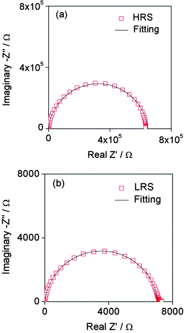 | ||
| Fig. 5 Impedance spectra of the Ni/Nb:SrTiO3/Ti stack in (a) the HRS and (b) the LRS. | ||
In the Schottky contact model, the value of the contact resistance is related to the height of the Schottky barrier and the width of the depletion layer. Considering all the experimental results presented in the above, we come up with a plausible switching mechanism. Different defects (e.g. oxygen vacancies) act as interface states in the interface.18,30 An interfacial layer inevitably exists on the Ni/Nb:SrTiO3 interface,28 and forms a potential drop Δ across the interfacial layer. The Schottky barrier height can be written as: ϕB = ϕM − χS − Δ. When a forward voltage is applied to the Ni/Nb:SrTiO3 interface, a large amount of electrons is extracted from the interface states, leading to an increase of Δ. This discharge effect decreases the Schottky barrier height and results in LRS. When a reverse voltage is applied, electrons are trapped in the interface states, and the Schottky barrier height increases, leading to the HRS. The amount of trapped/detrapped electrons in the interface states can be modified by controlling the magnitude of voltage or pulse,28 which induces different Schottky barrier heights, and thus different resistance states are obtained.
Conclusion
An unambiguous relationship between the resistance state and the Schottky barrier height is established, and the impedance spectroscopy investigations make such a relationship clearly visible. The variation of the Schottky barrier height can be attributed to charge trapping/detrapping in the interface states.Acknowledgements
This work is supported by the National Natural Science Foundation of China (Grant No. 51372094).Notes and references
- S. Q. Liu, N. J. Wu and A. Ignatiev, Appl. Phys. Lett., 2000, 76, 2749–2751 CrossRef CAS PubMed.
- X. Chen, N. Wu, J. Strozier and A. Ignatiev, Appl. Phys. Lett., 2006, 89, 063507 CrossRef PubMed.
- A. Beck, J. G. Bednorz, C. Gerber, C. Rossel and D. Widmer, Appl. Phys. Lett., 2000, 77, 139–141 CrossRef CAS PubMed.
- Z. B. Yan, Y. Y. Guo, G. Q. Zhang and J. M. Liu, Adv. Mater., 2011, 23, 1351–1355 CrossRef CAS PubMed.
- D. Pantel, S. Goetze, D. Hesse and M. Alexe, ACS Nano, 2011, 5, 6032–6038 CrossRef CAS PubMed.
- Y. Watanabe, J. G. Bednorz, A. Bietsch, C. Gerber, D. Widmer, A. Beck and S. J. Wind, Appl. Phys. Lett., 2001, 78, 3738–3740 CrossRef CAS PubMed.
- T. Fuji, M. Kawasaki, A. Sawa, H. Akoh, Y. Kawazoe and Y. Tokura, Appl. Phys. Lett., 2005, 86, 012107 CrossRef PubMed.
- D. Choi, D. Lee, H. Sim, M. Chang and H. Hwang, Appl. Phys. Lett., 2006, 88, 082904 CrossRef PubMed.
- S. Karg, G. I. Meijer, D. Widmer and J. G. Bednorz, Appl. Phys. Lett., 2006, 89, 072106 CrossRef PubMed.
- K. Szot, W. Speier, G. Bihlmayer and R. Waser, Nat. Mater., 2006, 5, 312–320 CrossRef CAS PubMed.
- M. Janousch, G. I. Meijer, U. Staub, B. Delley, S. F. Karg and B. P. Andreasson, Adv. Mater., 2007, 19, 2232–2235 CrossRef CAS.
- F. La Mattina, J. G. Bednorz, S. F. Alvarado, A. Shengelaya and H. Keller, Appl. Phys. Lett., 2008, 93, 022102 CrossRef PubMed.
- R. Waser and M. Aono, Nat. Mater., 2007, 6, 833–840 CrossRef CAS PubMed.
- R. Waser, R. Dittmann, G. Staikov and K. Szot, Adv. Mater., 2009, 21, 2632–2663 CrossRef CAS.
- A. Sawa, Mater. Today, 2008, 11, 28–36 CrossRef CAS.
- X. Guo, Appl. Phys. Lett., 2012, 101, 152903 CrossRef PubMed.
- Y. Aoki, C. Wiemann, V. Feyer, H. S. Kim, C. M. Schneider, H. I. Yoo and M. Martin, Nat. Commun., 2014, 5, 3473 Search PubMed.
- A. Sawa, T. Fujii, M. Kawasaki and Y. Tokura, Proc. SPIE, 2005, 5932, 59322C CrossRef PubMed.
- T. Menke, P. Meuffels, R. Dittmann, K. Szot and R. Waser, J. Appl. Phys., 2009, 105, 066104 CrossRef PubMed.
- J. Lee, E. M. Bourim, D. Shin, J. S. Lee, D. J. Seong, J. Park, W. Lee, M. Chang, S. Jung, J. Shin and H. Hwang, Curr. Appl. Phys., 2010, 10, e68–e70 CrossRef PubMed.
- Y. D. Xia, Z. G. Liu, W. Yang, L. Shi, L. Chen, J. Yin and X. K. Meng, Appl. Phys. Lett., 2007, 91, 102904 CrossRef PubMed.
- X. L. Jiang, Y. G. Zhao, Y. S. Chen, D. Li, Y. X. Luo, D. Y. Zhao, Z. Sun, J. R. Sun and W. H. Zhao, Appl. Phys. Lett., 2013, 102, 253507 CrossRef PubMed.
- C. H. Lai and C. Y. Liu, Appl. Phys. Lett., 2013, 103, 263505 CrossRef PubMed.
- N. T. Ho, V. Senthilkumar and Y. S. Kim, Solid-State Electron., 2014, 94, 61–65 CrossRef CAS PubMed.
- J. Robertson and C. W. Chen, Appl. Phys. Lett., 1999, 74, 1168–1170 CrossRef CAS PubMed.
- C. Park, Y. Seo, J. Jung and D. W. Kim, J. Appl. Phys., 2008, 103, 054106 CrossRef PubMed.
- S. M. Sze and K. K. Ng, Physics of Semiconductor Devices, Wiley, New Jersey, 3rd edn, 2007 Search PubMed.
- E. Mikheev, B. D. Hoskins, D. B. Strukov and S. Stemmer, Nat. Commun., 2014, 5, 3990 Search PubMed.
- M. C. Ni, S. M. Guo, H. F. Tian, Y. G. Zhao and J. Q. Li, Appl. Phys. Lett., 2014, 91, 183502 CrossRef PubMed.
- T. Shimizu and H. Okushi, J. Appl. Phys., 1999, 85, 7244–7251 CrossRef CAS PubMed.
- M. Yang, L. Z. Ren, Y. J. Wang, F. M. Yu, M. Meng, W. Q. Zhou, S. X. Wu and S. W. Li, J. Appl. Phys., 2014, 115, 134505 CrossRef PubMed.
- Y. Hikita, Y. Kozuka, K. Susaki, H. Takagi and H. Y. Wang, Appl. Phys. Lett., 2007, 90, 143507 CrossRef PubMed.
| This journal is © the Owner Societies 2015 |