The future of organic photovoltaics
Katherine A.
Mazzio
and
Christine K.
Luscombe
*
Materials Science and Engineering and Molecular Engineering and Sciences Institute, University of Washington, Seattle, WA, USA 98195. E-mail: luscombe@uw.edu
First published on 8th September 2014
Abstract
Increasing global demand for energy, along with dwindling fossil fuel resources and a better understanding of the hidden costs associated with these energy sources, have spurred substantial political, academic, and industrial interest in alternative energy resources. Photovoltaics based on organic semiconductors have emerged as promising low-cost alternatives for electricity generation that relies on sunlight. In this tutorial review we discuss the relevance of these organic photovoltaics beginning with some of the economic drivers for these technologies. We then examine the basic properties of these devices, including operation and materials requirements, in addition to presenting the development of the field from a historical perspective. Potential future directions are also briefly discussed. This tutorial review is intended to be an essential overview of the progress of the field, in addition to aiding in the discussion of the future of OPV technologies.
Key learning points(1) Why are we interested in organic photovoltaics (OPVs) and are they still relevant?(2) How does the photovoltaic process work, and how is device performance evaluated? (3) What are the most common device architectures and donor and acceptor materials used in the active layers for organic photovoltaics? (4) What is the importance of the active layer morphology and how can we control it? (5) What are the major obstacles or gaps in understanding that need to be addressed prior to the commercialization of OPV? |
1 Introduction
Interest in renewable energy resources has been gaining momentum in an effort to alleviate the global demand for fossil fuels due to their decreased availability and a greater understanding of the long-term effects of CO2 and other green house gas emissions. Global energy consumption is predicted to increase from approximately 17 TW in 2010 to approximately 27 TW by 2040, with the majority of projected demand coming from developing countries.1 While improvements in energy efficiency and conservation can help improve the global energy outlook by reducing the demand for fossil fuels, it is clear that investments in alternative energy resources are paramount to meeting future global energy needs. Photovoltaics are an established, though under-utilized, method for electricity generation. Fig. 1 shows the certified best efficiencies for a variety of photovoltaic technologies, with championship efficiencies for inorganic multijunction cells under solar concentration exceeding 44%, and with single crystalline silicon and multicrystalline silicon cells exceeding 25% and 20% efficiency, respectively.2 While these high efficiencies are promising, this is not the only metric for determining the potential value of these technologies. Perhaps the most important factor for the wide scale deployment of these technologies is their cost. These inorganic photovoltaic technologies overwhelmingly have production limitations due to direct competition for materials with the microelectronics industry, materials toxicity, high production costs due to the amount of material required for these devices and vacuum processing required for production, in addition to their high installation costs, which are directly linked to the weight of these cells. Organic photovoltaics based on π-conjugated polymers and small molecules have seen increasing interest in recent years as an alternative to inorganic photovoltaics because they offer a suite of promising properties. These include favorable electronic properties and component versatility, as well as low production and installation costs because they promise to be light-weight, solution processable, and applicable for large area and flexible devices.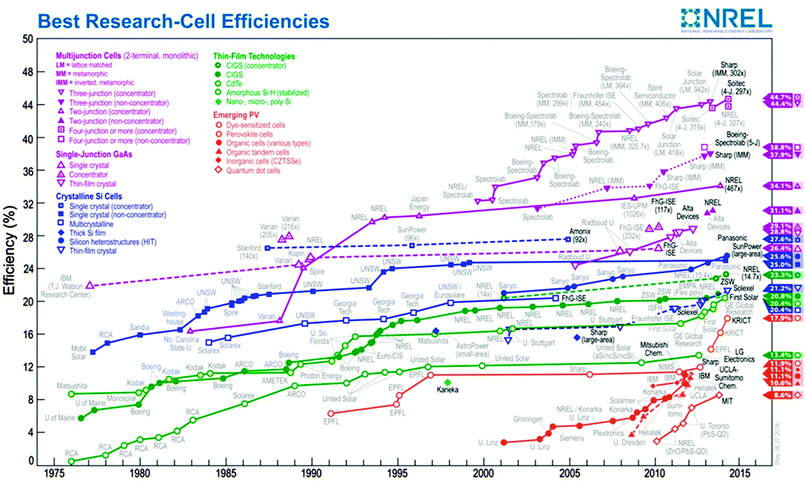 | ||
| Fig. 1 Certified best power conversion efficiencies over time for a variety of photovoltaic technologies, provided by NREL.2 This figure is current at the time of publication. Progress in photovoltaic power conversion efficiencies is tracked semi-annually by Green et al.50 | ||
Two metrics that are useful for evaluating and comparing these different photovoltaic technologies, in conjunction with their power conversion efficiency, include key economic indicators such as their Levelized Cost of Energy (LCOE) and their energy payback time (EPBT). The LCOE is a metric used to compare how cost-effective different types of energy sources are, with units of ¢ per kW h. It is determined by the ratio of the total life cycle cost, including all costs associated with construction, operation, maintenance, and decommission, and the total amount of energy produced over the lifetime of the system, as outlined according to eqn (1).
 | (1) |
The EPBT of a solar cell is the time required for a device to produce an amount of energy that is equivalent to the sum of the energy required to both manufacture and decommission that device. The EPBT has been investigated for various inorganic PV technologies available on the market, and several studies have also looked at potential EPBTs for organic PV.4 These calculations determine the EPBT as the ratio of the energy consumed over the life of the module and the energy that it generates over its lifetime. In order to do so, several assumptions must be made, including an average global insolation of approximately 1700 kW h m−2, and an average lifetime of 15 years for OPV, which is lower than the 20–30 year lifetime assumed for inorganic PV. These calculations also take into account energy efficiencies for each module, which are chosen to reflect devices that are currently at the manufacturing stage for inorganic photovoltaics, and forecasted efficiencies for organic photovoltaics that are not currently on the market. For mature technologies, such as mono- and poly-crystalline silicon photovoltaics, the EPBT has been estimated to be on the order of years.5 In contrast, the EPBT for organic photovoltaics, while being more difficult to predict due to their nature as an emerging technology, has been estimated to be on the order of days.4 For more specific details regarding the estimation of EPBT, the interested reader is referred to a recent article by Espinosa et al.4 While the forecasted efficiencies for OPV are quite low, they still have a short EPBT relative to their inorganic counterparts. This is a result of the same benefits discussed for reducing their LCOE: high throughput processing methods and reduced material consumption required during the manufacture of OPV relative to inorganic PV.
At present, OPV modules exhibit prohibitively low efficiencies and have issues associated with module stability and large scale materials manufacturing that need to be addressed prior to taking advantage of their many inherent benefits. Historically, increases in OPV device performance have been accompanied by breakthroughs in materials design or materials processing. In this tutorial review, we attempt to examine the advancement of the OPV field from a historical perspective in order to discuss issues that need to be addressed prior to the successful commercialization of OPV.
2 Device operating principles
2.1 The photovoltaic process
The photovoltaic process for OPV differs from that in inorganic photovoltaics. With inorganic materials, the absorption of photons with energies greater than the band gap results in the direct generation of free charge carriers (electrons and holes) that are able to separate at a p–n junction, where they may then diffuse under an externally applied electric field to their respective electrodes. Organic materials characteristically have a much lower dielectric constant than their inorganic counterparts, which prevents screening of the coulombic attraction between electrons and holes. This results in the generation of excitons, or coulombically bound electron–hole pairs upon photoabsorption, rather than free charge carriers. In order for these excitons to be useful in doing work through an external circuit, they must first be dissociated into free charge pairs. If the exciton is not able to dissociate within the lifetime of the exciton, the exciton will decay back to its ground state, resulting in the loss of that absorbed energy. In OPVs, exciton dissociation relies on the presence of a two-component system containing an electron donor and an electron acceptor that is similar to that of a p–n junction.6 The electron donor is typically characterized by a large ionization potential, while it is desirable for the electron acceptor to have a high electron affinity.Fig. 2 provides schematics of basic energy level diagrams used to describe OPV. The ionization potential (IP) of a neutral organic material is the energy required to remove an electron from its highest occupied molecular orbital (HOMO) to vacuum. The electron affinity (EA) is a measure of a materials ability to act as an electron acceptor, and is often approximated as the LUMO level relative to vacuum of an organic material. The HOMO–LUMO gap, or band gap, of a conjugated organic material is the minimum energy required to promote an electron from its HOMO to its LUMO. Fig. 2b shows representative work functions for anode and cathode materials in OPV, in addition to highlighting energetic offsets between donor and acceptor HOMO (ΔIP) and LUMO (ΔEA) levels, which are important for understanding charge transport mechanisms. Fig. 3 provides a simplified schematic of the photovoltaic process for OPV that is broken down into four steps. Upon photoabsorption, the first step, an electron can be excited from the donor HOMO to its LUMO, forming an exciton. This exciton must then diffuse to a donor/acceptor interface via a chemical potential gradient (step 2) where the electron can transfer to the LUMO of the acceptor material, forming a charge transfer (CT) complex, which will be favorable to occur when the energy difference between the donor LUMO and the acceptor LUMO (ΔEA) is greater than the binding energy of the exciton. This energy difference is typically on the order of a couple hundred meV, depending on the materials employed, and any absorbed energy in excess of this exciton binding energy will be lost in these systems. This is reflected by the theoretical maximum attainable voltage output of these cells being dictated by the difference between the donor HOMO and acceptor LUMO to a first approximation, and represents an important materials design consideration. The CT state can be described as having charge carriers that are coulombically bound across a donor/acceptor interface (referred to as geminate pairs), such that the energy of the CT state is highly dependent on the Coulombic attraction of the charge carriers, and in turn, on the distance that separates these species. The CT state can become a charge separated (CS) state, or free charge carriers, as step 3 in the photovoltaic process if the distance between the electron and hole becomes greater than the coulomb capture radius. However, if unable to escape the coulomb capture radius, the geminate pair will recombine across the donor/acceptor interface (referred to as geminate recombination), which is a competing process with free charge carrier generation and constitutes another loss mechanism in these devices. Any dissociated charges can then be transported through p-type or n-type domains to the electrodes, with holes being collected at the anode and electrons being collected at the cathode in step 4, where they can be used to do work in an external circuit. The final and leading loss mechanism in OPV is that of charge recombination, whereby free charge carriers recombine with unassociated charge carriers within a device, a process that is in direct competition with charge transport to the electrodes. A key objective in OPVs is the minimization of energy and charge loss processes in order to enhance the efficiency of devices. While the exciton dissociation process is actually far more complex than depicted, these simplified schematics are useful for generating a conceptual understanding of the photophysical processes occurring in OPVs. For a more detailed explanation of the charge photogeneration process, the reader is referred to an excellent review published by Clarke and Durrant in 2010.7
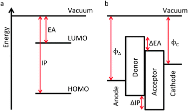 | ||
| Fig. 2 Basic energy level diagrams. (a) Of an organic semiconductor and (b) of a heterojunction solar cell. | ||
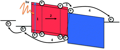 | ||
| Fig. 3 Schematic of the operating principles of OPV, highlighting the desired transport of charge pairs through the donor (red) and acceptor (blue) materials. | ||
2.2 Characterization of the photovoltaic effect
All photovoltaics are photodiodes, which are capable of generating current or voltage from incident light when operating in reverse bias (where the voltage at the anode is higher than that at the cathode) and can be described according to the equivalent circuit model, as shown schematically in Fig. 4a. In general, when a forward bias is applied to a diode, there is an exponential increase in current flow, whereas with the application of a reverse bias, there is a small saturation current that can be approximated as linear up to a large reverse bias voltage where breakdown will occur. In the dark, almost no current flows until large forward bias, and under ideal circumstances the applied bias is related to the current flow according to eqn (2). | (2) |
When under illumination, the J–V curve shifts down in an amount equal to the photocurrent, J, and the device can generate power. The maximum power point (MP) is the location on the J–V curve where the product of the current density and voltage is maximized. Under short circuit conditions (JSC), the current flow is at a maximum and there is no applied bias. The JSC is primarily dependent on factors related to the efficiencies of each stage in the photovoltaic process, including the efficiency of light absorption, exciton diffusion, exciton dissociation, charge transport, and charge collection. Open circuit conditions (VOC) characteristically have no current flow, and this is the point of maximum electrochemical potential of the cell. The VOC in inorganic photovoltaics is determined by the difference in the quasi Fermi levels of the p- and n-type junctions, while in organic photovoltaics, this value has been found to be dependent to a first approximation on the difference between the HOMO of the donor and the LUMO of the acceptor. Fig. 4b provides a schematic of the current density–voltage (J–V) response of a photodiode operating in the dark (dashed line) and under illumination (solid line).
The primary figure of merit for solar cells is the power conversion efficiency, ηe, which is the ratio of the maximum electrical power, Pm, generated by the device to the total incident optical power, Pin, and is defined according to eqn (3).
 | (3) |
 | (4) |
 | (5) |
The external quantum efficiency (EQE) is a measure of how much current will be produced by a particular wavelength of light and is given by the ratio of collected photogenerated charges and the number of incident photons. It is the probability that the absorption of one photon will result in the generation of one electron that is able to flow through an external circuit, and is typically integrated over the solar spectrum. The EQE describes the overall efficiency of the four main processes in the photovoltaic process for OPV, including absorption, exciton diffusion, charge separation, and charge collection, as defined by eqn (6).
| EQE(λ) = ηabs(λ) × ηdiff(λ) × ηCT(λ) × ηcoll(λ) | (6) |
Historically, test conditions for solar cells were not standardized, and there exist a variety of results in the early literature with seemingly inflated values due to discrepancies in testing conditions. Photovoltaics are now generally tested under standard conditions developed by the American Society for Testing and Materials (ASTM) in conjunction with research and development laboratories in order to influence reporting of comparable results.8 Briefly, laboratory testing is performed under the AM 1.5 G Solar spectrum, as outlined in Fig. 5, at an incident power of 1000 W m−2.9 The AM 1.5 G spectrum was developed for flat plate modules and represents the annual average solar irradiance at mid-latitudes, taking into account 1.5 times the thickness of Earth's atmosphere normal to the surface. In contrast, the AM 1.5 D spectrum was developed for use with solar concentrators, with an incident power of 900 W m−2 and includes not only the direct beam from the sun, but also a circumsolar component that accounts for a disk 2.5 degrees around the sun. Both of these standardized spectra have significantly reduced spectral irradiance relative to the top of the atmosphere, where the AM 0 solar spectrum, with an incident power of 1366 W m−2, will be of interest.
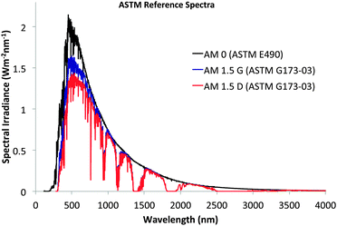 | ||
| Fig. 5 AM 0 (black), AM 1.5 G (blue), and AM 1.5 D (red) solar spectra.9 | ||
3 Device architectures
Because organic materials tend to require an energetic offset to dissociate excitons, attempts at using single layer architectures have been relatively unsuccessful, with these single layer device architectures affording efficiencies on the order of 0.1% or less.10 The seminal work of Tang in 1979 introduced the concept of a two component donor/acceptor active layer for organic photovoltaics that relied on layers of thermally evaporated small molecules.11,12 These bilayer structures were primarily limited by the exciton diffusion length, and only excitons generated near the donor/acceptor interface lived long enough to dissociate at this interface.13 This work paved the way for the development of other donor/acceptor type architectures with increased donor/acceptor interfacial areas, including the solution processed bulk-heterojunction (BHJ) type architecture, as first reported with a fullerene acceptor by Yu et al. in 1995, and which is considered the state of the art active layer morphology to this day.14 The BHJ architecture relies on finding a balance between charge generation and transport and can be limited by charge carrier lifetimes. Fig. 6 provides schematic illustrations of three common OPV device architectures, including standard BHJ, inverted BHJ, and tandem devices, each of which has its own benefits and areas that need improvement.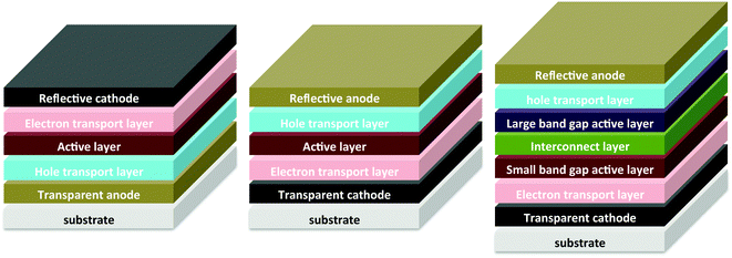 | ||
| Fig. 6 (left) Standard bulk heterojunction device architecture, (middle) inverted architecture, (right) tandem geometry. | ||
In a typical BHJ type solar cell,15 the active layer is sandwiched between an anode and a cathode, as outlined in Fig. 6 (left). With standard architectures, holes are transported to the anode and electrons are transported to the cathode. The anode in this case typically consists of a substrate that is coated with a high work function transparent conducting electrode, and modified with an interfacial hole selective/electron blocking layer between the electrode and the active layer. The most commonly observed materials in the OPV field used for these electrodes are tin-doped indium oxide (ITO) on glass substrates modified with a ∼40 nm thick poly(ethylenedioxythiophene):poly(styrene sulfonic acid) (PEDOT:PSS) interfacial layer. These materials are favorable due to their large optical transparency and good charge transport properties. There exist several issues with this combination, however, including the brittleness of both glass and ITO not allowing for roll to roll processing, the rarity and price of indium, and the acidity of PEDOT:PSS tending to degrade devices. The cathode is typically comprised of a low work function metal with an electron selective interlayer between the active layer and the metal electrode. The most frequently encountered cathode in the literature is aluminum, and popular interlayers have evolved over time, where LiF has waned in popularity with the rise of the Ca interlayer. The aluminum cathode is attractive due to its low work function and high reflectivity, but the low work function gives it highly reductive properties and it may react with polymers, or any water or oxygen in the system, resulting in an additional degradation pathway.
The inverted BHJ architecture was developed to help alleviate device degradation through both the use of different electrodes and encapsulation. The inverted architecture results in the reversal of the roles of the charge collecting nature of the electrodes. This effectively eliminates the need for a low work function, air-sensitive electrode, while simultaneously removing PEDOT:PSS from the ITO surface, which has been shown to introduce both chemical and morphological degradation at the ITO interface due to its acidic nature.16 The key to development of alternative architectures lies in the tunability of the ITO work function based on interlayer modifications. In the inverted structure, ITO is typically coated with a low work function material, such as ZnO or other transition metal oxides, in order to reduce its work function and make it applicable as the cathode. The anode typically consists of a stable metal, such as Ag or Au that is functionalized with a high work function transition metal oxide interlayer, such as V2O5 or MoO3, both of which exhibit better stability to oxidation. In addition to better stability, the inverted architecture is generally more compatible with high throughput processing and provides better flexibility for the development of tandem architectures.
Tandem architectures have been developed in order to address two specific issues associated with OPV. The first is in regard to the limits in active layer thickness that do not allow for a maximum amount of solar insolation to be absorbed, and which are imposed due to the relatively low charge carrier mobilities associated with the components of the active layer. The second relates to how the active layer materials absorb light, where any light not absorbed within the often narrow band gap of the organic absorber will be transmitted through the cell, and therefore lost. Tandem architectures consist of at least two independent active layers stacked on top of each other, one of which absorbs high-energy photons and transmits low energy photons through that can then be absorbed in another layer. Each independent active layer is separated from the other active layers by an interconnect layer that allows holes from one sub layer to recombine with electrons from another. Overall, the tandem structure is able to absorb more light because each layer can have complimentary absorption spectra, while maintaining relatively thin active layers, and is therefore not limited by the thickness of the active layer. It is desirable for each independent active layer in a tandem solar cell to deliver similar currents in order to maximize the efficiency of these devices. It has been hypothesized that tandem architectures should be able to produce 30% better efficiencies than their single junction counterparts. Tandem organic solar cell efficiencies have reached a 12% benchmark, as produced by Heliatek, and these devices are expected to exceed 15% efficiency in the near future.17
The development of alternative device architectures will continue to be important as the OPV field progresses towards commercialization. Each of the main architectures discussed has its own benefits, including the ease of processing and rich history of the standard BHJ architecture, the better stability and flexibility of the inverted architecture, and the better efficiency characteristics of the tandem architecture, but it is clear that more effort must be put forth in developing materials for each layer in these architectures in order to realize the commercialization of OPV. In the following section, we focus on the development of constituents for the active layer, leaving electrode and interlayer materials for the focus of other reviews.18
4 Design of electron donor and acceptor materials
Significant achievements have been made in OPV device performance through materials design, as the device performance parameters are highly dependent on the optical and electronic properties of the constituents of the active layer. The primary concerns for the development of effective donor and acceptor materials include developing materials with appropriate band gaps and energy levels in order to maximize both the JSC and VOC, promoting good charge carrier mobilities through the planarization of polymers along with good π–π stacking characteristics, and developing stable materials, all while maintaining their solution processability. Fig. 7 and 8 provide some examples of popular polymer and small molecule donor materials that have been used for OPV. In addition to producing polymers with good optoelectronic properties, other concerns for polymer design can include controlling the regioregularity, molecular weight, and dispersity of the polymers. The regioregularity of a polymer is defined as the ratio of monomers adopting head-to-tail (HT) coupling relative to those adopting head-to-head (HH) coupling in the polymer chain, as outlined in Fig. 7. It is an important property for polymers derived from asymmetrically substituted monomers, such as 3-hexylthiophene, but is not applicable for polymers synthesized with symmetric monomers. The molecular weight of a polymer is different than that of a small molecule, because polymer molecular weights comprise a molecular weight distribution due to how they are synthesized. The number average molecular weight, Mn, is defined as the total weight of all polymer molecules in a sample divided by the total number of polymer chains in that sample and is an important parameter for physical properties that are not dependent on the size distribution of the polymers, as described by eqn (7). | (7) |
 | (8) |
 | (9) |
Most of the materials used in the fledgling OPV community were designed for organic light emitting diode (OLED) applications, as this is where the majority of academic and industrial organic electronics research was focused at the time. As a result, popular OLED materials, such as poly(p-phenylene vinylene) based materials (PPVs) dominated the field in its early stages, and indeed, the first few points on the best research cell efficiency table in Fig. 1 reflect this polymer backbone. In 1995, Yu et al. used poly[2-methoxy-5-(2′-ethyl-hexyloxyl)-1,4-phenylene vinylene] (MEH-PPV) in combination with C60 and some of its functionalized derivatives, including phenyl-C61-butyric acid methyl ester (PCBM) in the first reported BHJ solar cells.14 Later, in 2001, Shaheen et al. used another PPV derivative, poly[2-methoxy-5-(3′,7′-dimethyloctyloxy)-1,4-phenylenevinylene] (MDMO-PPV) and PCBM to show the importance of active layer morphology on device performance, as discussed in the following section.19 During this time, significant improvements were achieved in the control of the synthetic reproducibility of these polymers, as well as in their regioregularity, molecular weight, and Đ. However, it became clear that the relatively large band gap of PPV-based materials, along with their low charge carrier mobilities would impose significant limitations on the maximum achievable power conversion efficiencies of photovoltaics made with these donor materials. As a result, interests shifted towards new polymer donor materials, especially poly(alkyl-thiophenes), including the now benchmark material poly(3-hexylthiophene) (P3HT).
 | ||
| Fig. 8 Examples of small band gap polymers and a small molecule, including different resonance structures. | ||
P3HT has proven to be a better material for OPV relative to PPVs due to its increased optical absorption, higher hole mobility, and its good solution processability. The performance of P3HT/PCBM solar cells depends critically on materials properties and processing conditions. The first encouraging results for P3HT/PCBM solar cells was published in 2002 by Schilinsky et al., who were able to make devices with a maximum EQE of 76%.20 This was followed by improving device performance in P3HT/PCBM solar cells via postproduction treatments by Padinger et al., who showed that thermal annealing and simultaneous thermal annealing and application of an external electric field could be used to produce devices with maximum PCE of 3.5%, as a result of better morphology.21 Kim et al. showed a strong dependence of the performance of P3HT/PCBM solar cells on the regioregularity of P3HT.22 They found that increasing the regioregularity of the polymer resulted in better performance as a result of increased molecular order due to better π–π stacking, resulting in both enhanced optical absorption and better charge transport properties. Schilinsky et al. showed the importance of molecular weight, by showing that P3HT/PCBM devices performed better as the molecular weight of P3HT increased.23 The increase in performance was primarily due to increased JSC, and this was attributed to an increased mobility with polymer aggregation in the thin films with higher molecular weight P3HT. While P3HT remains the most studied polymer for OPV, it has been recognized that a smaller band gap polymer with a lower HOMO, and greater hole mobilities would be required to advance the field.
Two popular ways to decrease the band gap of semiconducting polymers have arisen in recent years, including the development of polymers with alternating electron-rich and electron-poor heterocycles along the polymer backbone, or so-called donor/acceptor (D/A) type polymers, as well as through the stabilization of the quinoidal form of conjugated backbones. In D/A polymers, the decrease in band gap arises from the orbital mixing of these internal donor and acceptor units, as schematically illustrated in Fig. 8. One of the most successful examples of this type of D/A polymer is poly[N-9′-heptadecanyl-2,7-carbazole-alt-5,5-(4′,7′-di-2-thienyl-2′,1′,3′-benzothiadiazole)] (PCDTBT), which has 2,7-carbazole electron rich units and benzothiadiazole electron deficient units that are bridged by a conjugated thiophene unit, the combination of which results in an absorption spectrum that spans out to around 900 nm and devices made with this polymer have achieved efficiencies up to 7.5%.24 There exist two ground state resonance structures in highly conjugated polymers, including the aromatic and quinoidal forms, as shown schematically in Fig. 8. The quinoidal resonance structure promotes better planarity of the polymer backbone, enhancing charge carrier mobility, and has a smaller band gap than the aromatic resonance structure, providing better overlap with the highest photon flux in the solar spectrum, but this resonance is less energetically stable. Thienothiophene is perhaps the most popular unit used to promote the quinoidal form of a polymer, with PTB7 perhaps being most widely studied polymer in this class. PTB7 was reported by Liang et al. as the first polymer used in OPV to have a PCE exceeding 7%, and with further optimization has achieved over 9% efficiency.25,26 The high efficiency was primarily attributed to good JSC and FF, owing to both high EQE and IQE, which show that this system has excellent exciton dissociation, charge transport, and charge extraction characteristics, making this class of quinoidal stabilized polymers a promising class of donor materials for OPV.
While polymers have come to show tremendous promise for applications in OPVs, they tend to suffer from batch to batch variations, including disparities in molecular weight, end group contamination, and Đ. Small molecules have recently emerged as promising alternatives to polymers for OPV applications. In addition to consistency in the synthesis of small molecules, they also tend to exhibit higher hole and electron mobilities than their polymeric counterparts due to their propensity to exhibit long-range order. Sun et al. recently reported small molecule BHJ solar cells with efficiencies of up to 6.7% using the small molecule donor 5,5′-bis{(4-(7-hexylthiophen-2-yl)thiophen-2-yl)-[1,2,5]thiadiazolo[3,4-c]pyridine}-3,3′-di-2-ethylhexylsilylene-2,2′-bithiophene, or DTS(PTTh2)2, as outlined in Fig. 8.27 This small molecule donor is solution processable, strongly absorbing in the 600–800 nm region, exhibits high hole mobilities, and high power conversion efficiencies, showing that small molecules can be active competitors for OPV applications. For further reading on both solution processed and thermally evaporated small molecule organic solar cells, the interested reader is referred to a recent review by Mishra and Bäuerle.28
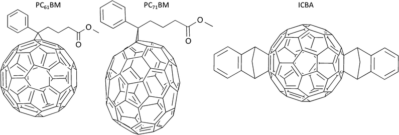
Much of the progress in OPV research has been focused on the donor materials, but the development of novel acceptor materials with stronger absorption in the visible region and tunable energy level alignments can improve both the JSC and VOC of the cell. The most common acceptor materials are fullerene derivatives, as outlined in Fig. 9. C60 is limited as an acceptor material due to its low solubility in common organic solvents, and as a result, the approach of adding solubilizing moieties to fullerenes has been adopted since the beginning of the field.14 PC61BM has traditionally been the most commonly used acceptor material, and has the advantages of good solubility in common organic solvents, high electron mobility, and a high electron affinity. However, PC61BM suffers from limited absorption in the visible region and a relatively deep LUMO, which limit its contribution to the JSC of the device and constrains the energy level requirements for donor materials in order to obtain high VOC. One approach to improve the acceptor characteristics is to replace PC61BM with its C70 derivative, PC71BM. PC71BM is less symmetric than its C60 analogue, and therefore has more allowed optical transitions, thus extending its absorption spectrum into the visible, where it can often provide a complimentary absorption profile to the donor materials, and significantly increase the overall JSC.29 PC71BM is the most common acceptor material used with low band gap donor polymers, and shows particular enhancement in performance when processed with small amounts of solvent additives that help promote idealized active layer morphologies, as discussed in the following section.25 Another approach is to adjust the LUMO level of the fullerene, thereby providing better energy level matching between donor and acceptor LUMO levels. The indene-C60 bis-adduct (ICBA), as first reported by He et al., is the most widely used fullerene taking advantage of this approach.30 It has a higher solubility in common organic solvents and is easier to synthesize than either PC61BM or PC71BM, in addition to having a LUMO level that is 0.17 eV higher than PC61BM. Initial P3HT/ICBA devices showed increases in VOC from 0.58 V to 0.84 V and PCE from 3.9% to 5.4% relative to P3HT/PC61BM devices, and confirmed the potential of ICBA as a potential acceptor material for OPV. For further information on fullerene derivatives in OPV, the interested reader is referred to a recent review by He and Li.31
5 Active layer morphology
Outside of materials development, one of the most fundamental issues in OPV processing is control of the active layer morphology. Indeed, extensive device optimization procedures have been followed since the beginnings of the field. A long-standing generalization is that the ideal active layer morphology will have an interpenetrating network of donor and acceptor materials, with domain sizes on the order of the exciton diffusion length, or around 10 nm.32,33 Essentially, the active layer should have enough interfacial area to dissociate the greatest possible amount of excitons, while also maintaining continuous charge transport pathways to the electrodes. However, as with most idealized principles for OPV operation, the reality is much more complex, and substantial efforts are being directed at understanding how to manipulate the microstructure of the active layer in order to generate desirable photovoltaic properties using a variety of materials and in a predictive manner. Typical parameters that affect the active layer morphology include the solvent, donor/acceptor concentrations, thermal annealing times and temperatures, solvent annealing conditions, additives, and the interlayer surface energies. The active layer morphology affects every device characteristic, and has recently been the study of extensive reviews.34–36 Here, we highlight some of long standing morphology optimization procedures, and discuss some recent developments in this area.Because the ability to be solution processed is considered integral for the success of OPV, it is important to understand how solvent choice affects the resulting morphology. Solvent properties, including the vapor pressure, boiling point, viscosity, polarity, solubility, and wettability characteristics dictate much of the initial film forming properties. The solute properties of the active layer components, including their concentrations, blend ratios, and solubility, are also important. Finally, the method of solution phase deposition is also important, as it is recognized that the requirements of high throughput processing will require alternatives to spin coating due to the large volume of materials and solvent and small areas required for this process. However, because it is the most widely used laboratory scale active layer deposition method, we will focus on the properties of spin coated active layers in this discussion.
In 2001, Shaheen et al. reported on the nearly three fold improvement of MDMO-PPV/PCBM devices by processing the active layer from chlorobenzene rather than toluene.19 They found that changing the solvent used for processing allowed for the formation of a more intimately mixed active layer with smaller domain sizes, which can be expected based on the better fullerene solubility in chlorobenzene. Hoppe et al. later performed a detailed study on the interplay between solvent, solvent loading, and blend composition.37 They used varying weight ratios of MDMO-PPV![[thin space (1/6-em)]](https://www.rsc.org/images/entities/char_2009.gif) :
:![[thin space (1/6-em)]](https://www.rsc.org/images/entities/char_2009.gif) PCBM of 1
PCBM of 1![[thin space (1/6-em)]](https://www.rsc.org/images/entities/char_2009.gif) :
:![[thin space (1/6-em)]](https://www.rsc.org/images/entities/char_2009.gif) 1, 1
1, 1![[thin space (1/6-em)]](https://www.rsc.org/images/entities/char_2009.gif) :
:![[thin space (1/6-em)]](https://www.rsc.org/images/entities/char_2009.gif) 2, 1
2, 1![[thin space (1/6-em)]](https://www.rsc.org/images/entities/char_2009.gif) :
:![[thin space (1/6-em)]](https://www.rsc.org/images/entities/char_2009.gif) 3, and 1
3, and 1![[thin space (1/6-em)]](https://www.rsc.org/images/entities/char_2009.gif) :
:![[thin space (1/6-em)]](https://www.rsc.org/images/entities/char_2009.gif) 4 in toluene and 1
4 in toluene and 1![[thin space (1/6-em)]](https://www.rsc.org/images/entities/char_2009.gif) :
:![[thin space (1/6-em)]](https://www.rsc.org/images/entities/char_2009.gif) 2, 1
2, 1![[thin space (1/6-em)]](https://www.rsc.org/images/entities/char_2009.gif) :
:![[thin space (1/6-em)]](https://www.rsc.org/images/entities/char_2009.gif) 4, and 1
4, and 1![[thin space (1/6-em)]](https://www.rsc.org/images/entities/char_2009.gif) :
:![[thin space (1/6-em)]](https://www.rsc.org/images/entities/char_2009.gif) 6 in chlorobenzene. They found that increasing the ratio of PCBM with films cast from toluene resulted in films with increasingly large PCBM aggregates that were surrounded by a thin skin of MDMO-PPV by cross-sectional SEM, as shown in Fig. 10. They also found that increasing the total polymer and fullerene content in the solution from 0.5% to 1.5% while maintaining the same weight ratio resulted in both increased film thickness and increased PCBM aggregation. When casting films from chlorobenzene, much better mixing of phases was observed for all weight ratios, and PCBM clustering was not observed until very high loading at 1
6 in chlorobenzene. They found that increasing the ratio of PCBM with films cast from toluene resulted in films with increasingly large PCBM aggregates that were surrounded by a thin skin of MDMO-PPV by cross-sectional SEM, as shown in Fig. 10. They also found that increasing the total polymer and fullerene content in the solution from 0.5% to 1.5% while maintaining the same weight ratio resulted in both increased film thickness and increased PCBM aggregation. When casting films from chlorobenzene, much better mixing of phases was observed for all weight ratios, and PCBM clustering was not observed until very high loading at 1![[thin space (1/6-em)]](https://www.rsc.org/images/entities/char_2009.gif) :
:![[thin space (1/6-em)]](https://www.rsc.org/images/entities/char_2009.gif) 6 MDMO-PPV
6 MDMO-PPV![[thin space (1/6-em)]](https://www.rsc.org/images/entities/char_2009.gif) :
:![[thin space (1/6-em)]](https://www.rsc.org/images/entities/char_2009.gif) PCBM, and even these clusters were much smaller than any of the clusters observed when processing from toluene. Li et al. showed that the solvent evaporation time will dictate the initial film properties, with slow evaporation allowing for phase separation of P3HT and PCBM, or fast evaporation resulting in the formation of an amorphous glass.38
PCBM, and even these clusters were much smaller than any of the clusters observed when processing from toluene. Li et al. showed that the solvent evaporation time will dictate the initial film properties, with slow evaporation allowing for phase separation of P3HT and PCBM, or fast evaporation resulting in the formation of an amorphous glass.38
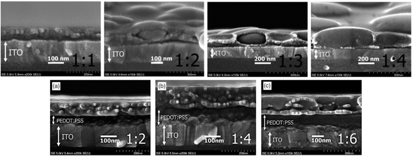 | ||
| Fig. 10 SEM cross sections of devices made with different MDMO-PPV:PCBM concentrations, as denoted in the bottom right of each image, and spun from (top) toluene and (bottom) chlorobenzene.37 Copyright 2004, Wiley. Used with permission from ref. 37, John Wiley and Sons. | ||
Both thermal and solvent annealing have been shown to be effective methods for modification of the active layer morphology, thereby influencing the overall device performance. Both types of annealing have been shown to result in the formation of larger P3HT and PCBM domains, and improve P3HT crystallization in P3HT/PCBM devices, resulting in the extension of the optical absorption into the red and improving the charge transport characteristics. Thermal annealing relies on heating substrates to temperatures greater than the glass transition temperature of the materials, thereby allowing them to reorient themselves to lower energy conformations. Two methods for thermal annealing have been investigated, including preannealing, where devices are annealed prior to cathode deposition, and postannealing, where devices are annealed after cathode deposition. Ma et al. performed a systematic study of postannealing temperatures and times and showed that the postannealing of P3HT/PCBM solar cells significantly improves both the JSC and FF, and they observed a decrease in the series resistance of the cell of more than an order of magnitude (from RS = 113 Ω cm2 to RS = 7.9 Ω cm2 with post annealing).39 Mihailetchi et al. showed that postannealing enhances the hole mobility of P3HT in P3HT/PCBM solar cells by three orders of magnitude, and that this boost in mobility is the most important factor for the observed increase in performance.40 They found that the generation of photocurrent in unannealed films is limited by the build-up of space charge, which is primarily a result of unbalanced charge carrier mobilities between P3HT and PCBM. After annealing above 110 °C, there was a 20-fold reduction in the difference between electron and hole mobilities, thereby reducing the space charge limitations due to the more balanced mobilities. Chen et al. used a variety of techniques, including GIXD, NEXAFS, and DSIMS, to determine how pre and postannealing affect the active layer morphology.41 They found that both annealing strategies resulted in the formation of a bicontinuous network of polymer and fullerene with domains on the order of the exciton diffusion length, and observed increased power conversion efficiencies for both cases (PCEs of 0.61%, 1.10%, and 3.37% for as spun, preannealed, and postannealed, respectively). However, the preannealed samples showed an increase in P3HT concentration near the surface of the active layer due to its lower surface energy, and a preferential packing of P3HT in an “edge on” fashion, both of which limited the improvement in device efficiency. In contrast, the postannealed samples showed an increase in PCBM concentration near the cathode and a reorientation of P3HT to the “face on” orientation, both of which promote efficient charge transfer, and are responsible for the greater improvement in device efficiency with postannealing rather than preannealing. The GIXD spectra highlighting the different propensities for edge on and face on polymer organization with the different annealing methods are shown in Fig. 11. The difference in postannealing response is a result of the importance of the difference in interfacial energies between the anode and the cathode.42
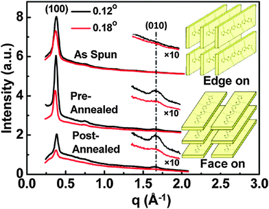 | ||
| Fig. 11 GIXD curves of P3HT/PCBM blend films at different incident angles. As spun; preannealed 30 min; postannealed 30 min. The insets represent the schemes of edge-on and face-on of P3HT chains.41 Reprinted with permission from ref. 41. Copyright 2011 American Chemical Society. | ||
Solvent annealing is an annealing approach that introduces solvent (through soaking) or solvent vapor into the active layer, making both components better able to diffuse through the active layer. This greater mobility promotes both better crystallization of P3HT and diffusion and segregation of PCBM. Choice of solvent is important when solvent annealing, and Cho et al. showed that poor solvents (acetone and methylene chloride) more greatly enhance device performance than good solvents (chloroform, 1,2-dichlorobenzene, chlorobenzene).43 While good solvents were shown to develop greater self-organization of P3HT, thus extending the optical absorption and promoting more balanced mobilities, the short circuit current density was found to be limited in this case by recombination losses due to the development of too large domains that were greater than the exciton diffusion length. Jo et al. used TOF-SIMS to show that solvent annealing promoted segregation of PCBM to the top of their devices, thus promoting better charge transport properties, similarly to those observed for thermal annealing.44 Chu et al. showed that solvent annealing more greatly enhances the EQE due to increased optical absorption relative to thermal annealing.45 Overall, both thermal and solvent annealing are important approaches for improving the crystallinity and vertical phase segregation within the active layer, increasing the hole mobility, and promoting more balanced charge transport characteristics, which makes annealing one of the most common approaches for enhancing device performance.
More recently, the development of novel low band gap polymers, such as poly[2,6-(4,4-bis-(2-ethylhexyl)-4H-cyclopenta[2,1-b;3,4-b′]-dithiophene)-alt-4,7-(2,1,3-benzothiadiazole)] (PCPDTBT), that do not respond well to annealing post-treatments have been reported. It has been found that using processing additives, such as alkanedithiols, can drastically improve the nanomorphology with these low band gap polymers.46 Lee et al. examined a series of 1,8-di(R)octanes with various functional (R) groups, and found that their best results were achieved with 1,8-di-iodooctane.47 This material preferentially dissolves PCBM, tends to remain in solution longer during drying, and therefore promotes the increased development of the PCBM domain, as schematically depicted in Fig. 12.47 They developed two general guidelines that have been identified for additive design: (1) the additive must have a significantly higher boiling point than the primary solvent in order to extend the interaction time of the additive and the components of the active layer during thin film formation, and (2) one of the active layer components should have a much higher solubility in the additive than the other material. The use of solvent additives has become one of the most important methods for controlling the development of crystalline domains with low band gap polymer solar cells.
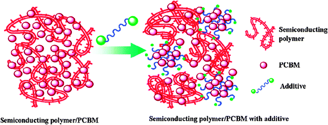 | ||
| Fig. 12 Schematic depiction of the role of the processing additive in the self-assembly of bulk heterojunction blend materials.47 | ||
An interpenetrating network of pure domains approximately 10 nm in diameter has been considered the ideal morphology for the active layer because it strikes a balance between promoting exciton dissociation at donor/acceptor interfaces and transporting charges through the bulk. Recently, however, it has been shown that considering a three phase system that includes crystalline regions of donor and acceptor materials as well as a mixed amorphous region is more realistic. Materials in the mixed region will characteristically have larger band gaps than those in the crystalline regions due to their amorphous nature, as outlined in Fig. 13.48 This mixed region necessitates changing our understanding of the energetic landscape of the bulk heterojunction architecture. With this three phase architecture, there is a clear driving force for exciton dissociation as well as imposed limitations for geminate recombination due to the energetic cascade caused by the mixed amorphous region. This supports the idea that the primary loss mechanism in BHJ solar cells arises from charge recombination, rather than geminate recombination or exciton decay. This mixed region was first indicated by Watts et al. in 2009 when they described the partial miscibility of PCBM in P3HT.49 It has since become ubiquitous in the field when discussing the active layer microstructure.
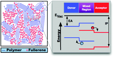 | ||
| Fig. 13 Schematic of a BHJ solar cell including the mixed region. Potential shifts in the local energetic landscape at the border between the donor, mixed and acceptor phases are shown in detail. EA is the electron affinity, IP is the ionization potential.48 Copyright 2013, Wiley. Used with permission from ref. 48, John Wiley and Sons. | ||
6 Conclusion and outlook
Much progress has been made in materials development and understanding the structure–property relationships of OPV materials and devices, but there are still many improvements that need to occur prior to the wide scale manufacture of OPV. Following with the LCOE model, it is clear that improvements need to be made in increasing device efficiency, improving device lifetime, and lowering the cost of devices. While laboratory scale devices have recently been made with efficiencies over 9% in the single junction architecture and over 12% with a multijunction approach, there remains a significant drop in efficiency on the module scale.17,26 Consequently, there is a strong need to improve module efficiencies, including identifying ways to translate lab scale performance to roll to roll processing and designing large-area modules that are able to reduce electrical losses. The stability of these devices will also need to be improved in parallel. This will require a greater understanding of the interactions at all of the interfaces of a given cell architecture, as well as improvements at both the material and device architecture levels of water and oxygen stability. Finally, the identification of materials that meet the above goals will necessitate large-scale production of these materials with limited batch-to-batch variation in addition to the utilization of these materials in high throughput processes.Currently, OPVs are applicable only in niche markets that require lightweight, flexibility, and variable angle performance, such as in the consumer electronics market. However, the continued development of inverted and tandem device architectures, as well as improvement in the light harvesting ability and morphology control of active layer materials will result in widely applicable OPV technologies for electricity generation. Key economic indicators suggest that OPVs will become competitive with traditional energy sources as a result of a low LCOE and outstanding EPBT due to their lightweight and high-throughput, roll-to-roll solution processing, and the rapid progress of this field instills continued confidence in this technology.
Acknowledgements
The authors are grateful for financial support from NSF EFRI SEED 1038165 and NSF DMR 1407815.References
- International Energy Outlook 2013 - Energy Information Administration http://www.eia.gov/forecasts/ieo.
- NREL Best Research-Cell Efficiencies http://www.nrel.gov/ncpv/images/efficiency_chart.jpg.
- 2013 Technology Map of the European Strategic Energy Technology Plan, JRC Science and Policy Report http://setis.ec.europa.eu/system/files/2013TechnologyMap.pdf.
- N. Espinosa, M. Hösel, D. Angmo and F. C. Krebs, Energy Environ. Sci., 2012, 5, 5117 CAS
.
- K. Knapp and T. Jester, Sol. Energy, 2001, 71, 165–172 CrossRef CAS
.
- N. S. Sariciftci, L. Smilowitz, A. J. Heeger and F. Wudl, Science, 1992, 258, 1474–1476 CAS
.
- T. M. Clarke and J. R. Durrant, Chem. Rev., 2010, 110, 6736–6767 CrossRef CAS PubMed
.
- ASTM E984 - 09 Standard Test Method for Electrical Performance of Photovoltaic Cells Using Reference Cells Under Simulated Sunlight http://enterprise.astm.org/filtrexx40.cgi?+REDLINE_PAGES/E948.htm.
- ASTM G173 - 03 Reference Spectra http://rredc.nrel.gov/solar/spectra/am1.5/.
- S. Karg, W. Riess, V. Dyakonov and M. Schwoerer, Synth. Met., 1993, 54, 427–433 CrossRef CAS
.
-
C. W. Tang, US Pat., 4164431 A, 1979 Search PubMed
.
- C. W. Tang, Appl. Phys. Lett., 1986, 48, 183 CrossRef CAS PubMed
.
- J. J. M. Halls, K. Pichler, R. H. Friend, S. C. Moratti and A. B. Holmes, Appl. Phys. Lett., 1996, 68, 3120 CrossRef CAS PubMed
.
- G. Yu, J. Gao, J. C. Hummelen, F. Wudl and A. J. Heeger, Science, 1995, 270, 1789–1791 CAS
.
- S. H. Park, A. Roy, S. Beaupré, S. Cho, N. Coates, J. S. Moon, D. Moses, M. Leclerc, K. Lee and A. J. Heeger, Nat. Photonics, 2009, 3, 297–302 CrossRef CAS
.
- M. P. de Jong, L. J. van IJzendoorn and M. J. A. de Voigt, Appl. Phys. Lett., 2000, 77, 2255 CrossRef CAS PubMed
.
- Heliatek Press release, January 16, 2013 http://www.heliatek.com/newscenter/latest_news/neuer-weltrekord-fur-organische-solarzellen-heliatek-behauptet-sich-mit-12-zelleffizienz-als-technologiefuhrer/?lang=en .
- K. Ellmer, Nat. Photonics, 2012, 6, 809–817 CrossRef CAS
.
- S. E. Shaheen, C. J. Brabec, N. S. Sariciftci, F. Padinger, T. Fromherz and J. C. Hummelen, Appl. Phys. Lett., 2001, 78, 841 CrossRef CAS PubMed
.
- P. Schilinsky, C. Waldauf and C. J. Brabec, Appl. Phys. Lett., 2002, 81, 3885 CrossRef CAS PubMed
.
- F. Padinger, R. S. Rittberger and N. S. Sariciftci, Adv. Funct. Mater., 2003, 13, 85–88 CrossRef CAS
.
- Y. Kim, S. Cook, S. M. Tuladhar, S. A. Choulis, J. Nelson, J. R. Durrant, D. D. C. Bradley, M. Giles, I. McCulloch, C.-S. Ha and M. Ree, Nat. Mater., 2006, 5, 197–203 CrossRef CAS
.
- P. Schilinsky, U. Asawapirom, U. Scherf, M. Biele and C. J. Brabec, Chem. Mater., 2005, 17, 2175–2180 CrossRef CAS
.
- D. H. Wang, J. K. Kim, J. H. Seo, I. Park, B. H. Hong, J. H. Park and A. J. Heeger, Angew. Chem., Int. Ed., 2013, 52, 2874–2880 CrossRef CAS PubMed
.
- Y. Liang, Z. Xu, J. Xia, S.-T. Tsai, Y. Wu, G. Li, C. Ray and L. Yu, Adv. Mater., 2010, 22, E135–E138 CrossRef CAS PubMed
.
- Z. He, C. Zhong, S. Su, M. Xu, H. Wu and Y. Cao, Nat. Photonics, 2012, 6, 593–597 CrossRef CAS
.
- Y. Sun, G. C. Welch, W. L. Leong, C. J. Takacs, G. C. Bazan and A. J. Heeger, Nat. Mater., 2012, 11, 44–48 CrossRef CAS PubMed
.
- A. Mishra and P. Bäuerle, Angew. Chem., Int. Ed., 2012, 51, 2020–2067 CrossRef CAS PubMed
.
- M. M. Wienk, J. M. Kroon, W. J. H. Verhees, J. Knol, J. C. Hummelen, P. A. van Hal and R. A. J. Janssen, Angew. Chem., Int. Ed., 2003, 42, 3371–3375 CrossRef CAS PubMed
.
- Y. He, H.-Y. Chen, J. Hou and Y. Li, J. Am. Chem. Soc., 2010, 132, 1377–1382 CrossRef CAS PubMed
.
- Y. He and Y. Li, Phys. Chem. Chem. Phys., 2011, 13, 1970–1983 RSC
.
- D. E. Markov, E. Amsterdam, P. W. M. Blom, A. B. Sieval and J. C. Hummelen, J. Phys. Chem. A, 2005, 109, 5266–5274 CrossRef CAS PubMed
.
- M. Sim, J. Shin, C. Shim, M. Kim, S. B. Jo, J.-H. Kim and K. Cho, J. Phys. Chem. C, 2014, 118, 760–766 CAS
.
- L.-M. Chen, Z. Hong, G. Li and Y. Yang, Adv. Mater., 2009, 21, 1434–1449 CrossRef CAS
.
- K. Vandewal, S. Himmelberger and A. Salleo, Macromolecules, 2013, 46, 6379–6387 CrossRef CAS
.
- F. Liu, Y. Gu, J. W. Jung, W. H. Jo and T. P. Russell, J. Polym. Sci., Part B: Polym. Phys., 2012, 50, 1018–1044 CrossRef CAS
.
- H. Hoppe, M. Niggemann, C. Winder, J. Kraut, R. Hiesgen, A. Hinsch, D. Meissner and N. S. Sariciftci, Adv. Funct. Mater., 2004, 14, 1005–1011 CrossRef CAS
.
- G. Li, Y. Yao, H. Yang, V. Shrotriya, G. Yang and Y. Yang, Adv. Funct. Mater., 2007, 17, 1636–1644 CrossRef CAS
.
- W. Ma, C. Yang, X. Gong, K. Lee and A. J. Heeger, Adv. Funct. Mater., 2005, 15, 1617–1622 CrossRef CAS
.
- V. D. Mihailetchi, H. X. Xie, B. de-Boer, L. J. A. Koster and P. W. M. Blom, Adv. Funct. Mater., 2006, 16, 699–708 CrossRef CAS
.
- D. Chen, A. Nakahara, D. Wei, D. Nordlund and T. P. Russell, Nano Lett., 2011, 11, 561–567 CrossRef CAS PubMed
.
- M. Campoy-Quiles, T. Ferenczi, T. Agostinelli, P. G. Etchegoin, Y. Kim, T. D. Anthopoulos, P. N. Stavrinou, D. D. C. Bradley and J. Nelson, Nat. Mater., 2008, 7, 158–164 CrossRef CAS PubMed
.
- J. H. Park, J. S. Kim, J. H. Lee, W. H. Lee and K. Cho, J. Phys. Chem. C, 2009, 113, 17579–17584 CAS
.
- J. Jo, S.-I. Na, S.-S. Kim, T.-W. Lee, Y. Chung, S.-J. Kang, D. Vak and D.-Y. Kim, Adv. Funct. Mater., 2009, 19, 2398–2406 CrossRef CAS
.
- C.-W. Chu, H. Yang, W.-J. Hou, J. Huang, G. Li and Y. Yang, Appl. Phys. Lett., 2008, 92, 103306 CrossRef PubMed
.
- J. Peet, J. Y. Kim, N. E. Coates, W. L. Ma, D. Moses, A. J. Heeger and G. C. Bazan, Nat. Mater., 2007, 6, 497–500 CrossRef CAS PubMed
.
- J. K. Lee, W. L. Ma, C. J. Brabec, J. Yuen, J. S. Moon, J. Y. Kim, K. Lee, G. C. Bazan and A. J. Heeger, J. Am. Chem. Soc., 2008, 130, 3619–3623 CrossRef CAS PubMed
.
- T. M. Burke and M. D. McGehee, Adv. Mater., 2014, 26, 1923–1928 CrossRef CAS PubMed
.
- B. Watts, W. J. Belcher, L. Thomsen, H. Ade and P. C. Dastoor, Macromolecules, 2009, 42, 8392–8397 CrossRef CAS
.
- M. A. Green, K. Emery, Y. Hishikawa, W. Warta and E. D. Dunlop, Prog. Photovoltaics, 2014, 22, 701–710 Search PubMed
.
| This journal is © The Royal Society of Chemistry 2015 |

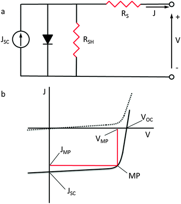
![[dash dash, graph caption]](https://www.rsc.org/images/entities/char_e091.gif) ; illuminated, -). The characteristic intersections with the abscissa and ordinate are the open circuit voltage (
; illuminated, -). The characteristic intersections with the abscissa and ordinate are the open circuit voltage (
