Factors affecting bismuth vanadate photoelectrochemical performance†
Timothy S.
Sinclair
,
Bryan M.
Hunter
,
Jay R.
Winkler
,
Harry B.
Gray
and
Astrid M.
Müller
*
Beckman Institute and Division of Chemistry and Chemical Engineering, California Institute of Technology, Pasadena, California 91125, USA. E-mail: astridm@caltech.edu
First published on 2nd December 2014
Abstract
Bismuth vanadate is a promising photoanode material, but recent reports on undoped BiVO4 without sublayers and co-catalysts showed large variations in photocurrent generation. We addressed this issue by correlating photoelectrochemical performance with physical properties. We devised a novel anodic electrodeposition procedure with iodide added to the aqueous plating bath, which allowed us to prepare BiVO4 photoanodes with virtually identical thicknesses but different morphologies, and we could control surface Bi content. Morphologies were quantified from SEM images as distributions of crystallite areas and aspect-ratio-normalised diameters, and their statistical moments were derived. We could obtain clear photocurrent generation trends only from bivariate data analysis. Our experimental evidence suggests that a combination of low Bi/V ratio, small aspect-ratio-normalised diameters, and crystallites sizes that were small enough to provide efficient charge separation yet sufficiently large to prevent mass transport limitations led to highest photoelectrochemical performance.
Conceptual insightsDiscovery of robust, efficient, and scalable light absorbers and redox catalysts that can be employed in integrated photoelectrodes to produce solar fuels is one of the grand challenges of 21st century science. Among candidates containing earth abundant elements, bismuth vanadate is a particularly promising material, most especially as a light-absorber photoanode component for solar-driven water splitting. In our work, we have established how the physical properties of BiVO4 photoanodes affect performance by systematic study of morphologies and chemical surface compositions in combination with photocurrent measurements. Optimized photocurrent generation of BiVO4 photoanodes resulted from intertwined material properties, whose interplay was probed by bivariate data analysis. Most notably, optimal morphologies and chemical surface compositions were identified, enabling rational design of more efficient BiVO4 photoanodes. |
Introduction
Conversion of solar energy into storable chemical fuels will in the future be essential as a global, environmentally friendly energy source.1 Splitting water with only sunlight as the energy input into hydrogen fuel and oxygen in a sustainable, scalable way requires that materials be exclusively made of earth-abundant elements.2–9 Viable renewable energy systems will only be feasible with materials that are robust in water oxidation or hydrogen evolution conditions, efficient light absorbers, and highly active chemical catalysts. Integrated devices, which couple electrocatalysts with light-capturing semiconductors, with a membrane that separates the two half reactions of water splitting, show particular promise.10,11 Because of the greater stability of earth-abundant water-oxidation catalysts at higher pH,12–14 we focused on alkaline electrolytes.Semiconducting photoanodes must exhibit a bandgap that is small enough for efficient absorption of sunlight and a valence band edge that is positive enough for the generation of overpotentials sufficient to drive water oxidation. The flatband potential of the photoanode also matters as it determines the photocurrent onset potential of the water oxidation reaction.10
Based on these constraints, bismuth vanadate (BiVO4) has recently been identified as an inexpensive, promising photoanode material for solar water splitting.15–21 However, typical photocurrents of unmodified BiVO4 photoanodes are limited by high electron–hole recombination and poor charge transport properties,16,22–24 and inadequate water oxidation kinetics.15
Although photoelectrochemical (PEC) performance of BiVO4 photoanodes can be improved by dopants, sub-layers, addition of water oxidation catalysts, (see ref. 15 and references therein), incorporation of dopant nanoparticles,25 hydrogenation,26 incorporation with reduced graphene oxide,27 underlayers with improved band edge alignment,28,29 and substrates with enhanced light-capture properties,30 we focused our work on unmodified BiVO4 films deposited directly on inexpensive fluorine-doped tin oxide (FTO) glass substrates. This way, we could systematically investigate photocurrent generation as a function of the physical characteristics of BiVO4 itself, with the aim to differentiate contributions from different properties.
Multiple methods to make undoped BiVO4 photoanodes on various conducting oxide substrates have been reported ((ESI), Table S1†). Likewise, photocurrents have been measured in numerous different solution conditions, with different scan rates, and on different transparent conducting oxide substrates, rendering a direct comparison of reported performance problematic. Published photocurrent densities of monoclinic scheelite BiVO4 films in electrolytes without hole acceptors range from ∼0.1 to 1.8 mA cm−2 (at 1 sun, AM1.5G illumination and at 1.23 V vs. RHE); in different electrolytes without and with sacrificial hole acceptor large variations have been observed (see Table S1†).
To identify the materials' characteristics that limit photocurrent generation, we synthesised undoped BiVO4 films on FTO-glass with various physical properties. We employed two solution-based fabrication techniques, spin-coating and electrodeposition, and varied only one experimental parameter at a time. All films were subjected to the same annealing temperatures in ambient air and tested for photocurrent generation under virtually identical conditions. Spin-cast BiVO4 photoanodes were prepared with four different numbers of spin-coating cycles following a procedure reported by Gamelin.31 In addition, we increased the viscosity of the precursor solution by adding polyethylene glycol. Electrodeposited BiVO4 films on FTO-glass were prepared following a procedure published by Choi.32 We also devised a modification of that preparation by addition of iodide to the plating bath to improve the solubility of Bi3+ ions.
Best performing crystallite sizes and film thicknesses are usually a trade-off between several factors. Crystallite sizes should be smaller than the minority carrier diffusion length to maximise electron–hole separation efficiency. Granular materials, such as those investigated here, exhibit many interfaces that create contacts and junctions throughout the bulk of the BiVO4 films. As crystallites become smaller, more interfaces and space-charge regions are present, at which photo-generated minority carriers can be collected; in other words, the internal quantum yield approaches unity when every crystallite is completely depleted. However, added interfaces, i.e. more contact points between crystallites, decrease the minority carrier mobility, so that carrier collection efficiency competes with bulk recombination. Majority carrier mobility is also affected and may ultimately be limiting photocurrent generation.3,29 Moreover, the high porosity of materials with small crystallite sizes limits mass transport of substrates and products. And thicker semiconducting layers absorb more incident photons until the ray-optic limit is reached.33 Light capture can also be increased by strategic sub-wavelength nanostructuring.34 This is the reason why BiVO4 photoanodes made on textured Asahi VU-type conducting glass substrate outperform those on standard, inexpensive FTO-glass (such as Hartford Glass Co., TEC 15).30 Because most reported studies on undoped BiVO4 photoanode performance were carried out on standard FTO-glass, we synthesised our BiVO4 films on TEC-15 FTO substrates.
In addition to charge separation efficiency at the BiVO4–electrolyte interface, crystallite size also affects interfacial electrical contact between the BiVO4 and the conducting oxide substrate. Lattice mismatches between fluorine-doped tin oxide or tin-doped indium oxide (ITO) substrates and BiVO4 attenuate electrical contact. The use of different types of conducting oxide substrates renders a direct comparison of reported BiVO4 PEC performance problematic (ESI†).
We measured photocurrent densities of our BiVO4 photoanodes in alkaline aqueous supporting electrolyte under simulated 1 sun AM1.5G illumination. We collected linear sweep and cyclic voltammograms with and without illumination. There is still debate on the exact mechanisms behind the observation of different PEC responses from front-side vs. back-side illumination. This difference may disappear if the layer thickness approaches the diffusion length of the carriers with lower mobility in the material. However, highest photocurrents and negligible differences between the two illumination modes were observed for BiVO4 films with 100 nm and 300 nm thickness.16,23 Regarding practical considerations, for use in an integrated water splitting device, only front-side illumination will matter. Therefore, we performed our PEC testing with front-side illumination.
In this work, we aimed to explain the considerable PEC performance variations reported for unmodified BiVO4 photoanodes. We probed the complex interplay of multiple materials characteristics, such as morphology, chemical surface composition, and film thickness, and related them to photocurrent generation.
Experimental section
BiVO4 photoanodes were prepared by electrodeposition or spin coating on FTO-glass substrates. Films were physically characterised as follows: thicknesses were derived from optical spectra using absorption coefficients reported for powder BiVO4,35 crystalline phases from powder X-ray diffraction (XRD) data, chemical surface compositions from X-ray photoelectron spectra (XPS), and morphologies were quantified by scanning electron microscopy (SEM) image analysis. Photoelectrochemical performance was assessed under 1 sun AM1.5G illumination in alkaline supporting electrolytes without and with sulfite as sacrificial hole acceptor. See ESI† for details.Results and discussion
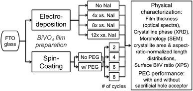
The general protocol to prepare and characterise BiVO4 photoanodes is depicted in Fig. 1. We used electrodeposition and spin coating and systematically varied conditions to make BiVO4 films on FTO-glass with numerous thicknesses, morphologies, and chemical surface compositions.Bulk crystalline phases of the BiVO4 on FTO-glass films were determined by powder XRD (ESI†); peak assignment was performed using the International Centre for Diffraction Data (ICDD) database. All obtained films were found to consist of monoclinic scheelite BiVO4; this crystalline phase is the most photoactive polymorph of bismuth vanadate.17,18 XRD data of all BiVO4 on FTO-glass films showed peaks assigned to SnO2 from the FTO substrate underneath because the films were thin, but no secondary phases of BiVO4 and no bismuth or vanadium oxide phases were observed.
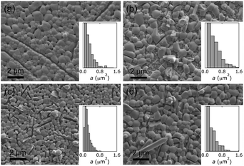
Inspection of SEM images showed that all our BiVO4 films exhibited pillow-like crystallites. These shapes were best approximated by ellipses with various aspect ratios. Top-down SEM images provided views of the surface-exposed crystallites, projected by the focusing conditions and threshold transformation onto one plane. Therefore, we used area distributions to describe crystallite sizes, which are shown as insets in Fig. 2 and 5.
We also deduced distributions of crystallite diameters, which were normalised to their aspect ratios; this way we could address the effect of varying aspect ratios of the crystallites that were not captured by mere area distributions. Aspect ratios are important for carrier transport because they are directly related to the nearest distances between any point within a crystallite and that crystallite's edge. Upon absorption of a photon an electron–hole pair may be generated anywhere within a crystallite. Assuming isotropic carrier dynamics within the material, the nearest distance of the original location of this electron–hole pair to the boundary of the crystallite controls whether useful carrier collection or detrimental recombination loss is more likely. The aspect ratio of an ellipse is its semi-major axis divided by its semi-minor axis. To describe distances that are relevant for carrier transport, we derived distributions of the aspect-ratio-normalised diameters l from SEM image analysis; l is the square root of a crystallite's area normalised to its aspect ratio, or, in other words, an ellipse's semi-minor axis divided by its semi-major axis times the square root of its area. If crystallites have laterally circular shapes, l is equal to the square root of a; l becomes smaller as the aspect ratio increases. The mean values of a and l are denoted A and L, respectively.
Analysis of the statistical moments of the area and aspect-ratio-normalised diameters indicated that spin coating afforded films of more uniform distributions (i.e., Gaussian). All distributions showed a variance (σ2) that was approximately proportional to the mean size. Positive, relatively small values for the third moment indicated that populations were skewed with a modest number of crystallites significantly larger than the mean. In other words, crystallites with values of a and l larger than the population means were present, albeit in very small relative quantity.
In general, charge separation efficiency is enhanced when L decreases, i.e. small crystallite areas and high aspect ratios are beneficial for this purpose. Mass transport limitations become a major obstacle for photocurrent enhancement by simply shrinking crystallite size. Therefore, high-aspect-ratio architectures are desirable. On the other hand, the size A of BiVO4 crystallites governs the electrical contact at the interface between BiVO4 and FTO, owing to the crystal lattice mismatch between the two oxides (ESI†); the number of point contacts at the interface to the cuboid FTO increases as A decreases.
Electrodeposited films were made following a procedure by Choi,32 and, as a modification of that, with varying amounts of NaI added to the deposition bath. All other conditions were kept virtually identical. Addition of iodide improved the solubility of Bi3+ ions in aqueous solution by formation of [BiI4]−; this required a fourfold excess of iodide ions over Bi3+ ions. Therefore, we chose [I−]/[Bi3+] ratios of 4, 8, and 12 in the plating bath.
Without NaI, the deposition solution became turbid as soon as the pH was adjusted with acetate to reach deposition conditions. With addition of iodide, we did not observe any precipitate throughout the plating process; solutions remained precipitate-free for hours (ESI†). The obtained films had markedly different morphologies, as shown by SEM images (Fig. 2).
We did not observe any contributions from crystalline BiOI in the powder XRD spectra of BiVO4 materials that were anodically deposited in plating baths with NaI. Likewise, high-resolution XPS data of the I 3d core level region revealed that no iodine photoelectrons were detectable (ESI†). It should be noted that formation of BiOI, such as that reported by Choi,36 is possible under cathodic electrodeposition conditions.
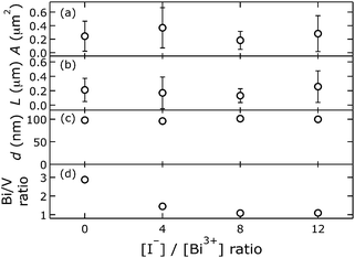
All four electrodeposited materials had similar thicknesses of (99 ± 2) nm. The only difference in preparation conditions was the iodide concentration in the plating bath; also, virtually identical amounts of charge were passed. Despite having similar thicknesses, these BiVO4 films exhibited markedly different morphologies and chemical surface compositions. Survey XPS data (ESI†) showed the presence of elemental Bi, V, and O. We deliberately did not attempt to quantify oxygen content from XPS data because the amount of this element is regularly overestimated; oxygen also occurs in other sources, such as adventitious carbon species and underlying conductive oxide. High-resolution spectra of the Bi 4d and V 2p core level regions showed that each spin–orbit split peak (Bi 4d5/2, Bi 4d3/2, V 2p3/2, and V 2p1/2) could be fitted by a single Gaussian–Lorentzian component. This indicates that in all electrodeposited BiVO4 films Bi and V were present in a single oxidation state. The Bi 4d core level peaks Bi 4d5/2 and Bi 4d3/2 had binding energies of 442.6 and 466.0 eV, respectively, with an expected branching ratio of 1.5![[thin space (1/6-em)]](https://www.rsc.org/images/entities/char_2009.gif) :
:![[thin space (1/6-em)]](https://www.rsc.org/images/entities/char_2009.gif) 1, and were assigned to Bi3+.37 The V 2p region consisted of V 2p3/2 and V 2p1/2 components with binding energies of 516.9 and 524.3 eV, respectively, with an expected branching ratio of 2
1, and were assigned to Bi3+.37 The V 2p region consisted of V 2p3/2 and V 2p1/2 components with binding energies of 516.9 and 524.3 eV, respectively, with an expected branching ratio of 2![[thin space (1/6-em)]](https://www.rsc.org/images/entities/char_2009.gif) :
:![[thin space (1/6-em)]](https://www.rsc.org/images/entities/char_2009.gif) 1, allowing assignment to V5+.38,39 Our XPS data confirmed that all electrodeposited films consisted of BiVO4.
1, allowing assignment to V5+.38,39 Our XPS data confirmed that all electrodeposited films consisted of BiVO4.
Surface Bi/V ratios were quantified by integrating Bi 4d5/2 and V 2p3/2 peaks of high-resolution XPS spectra after Shirley background subtraction.40 We chose to collect high-resolution data in the Bi 4d over the Bi 4f core level region, which is often used for qualitative characterization, because at the higher binding energy the background is free of other (broad) peaks; this facilitates a quantitative chemical composition analysis. We observed that surface Bi/V ratios varied from 2.9 to 1.1, as a function of the amount of NaI in the plating bath (Fig. 3). Apparently, improving the solubility of Bi3+ in the plating bath led to less excess Bi at the surface.
Morphology quantification led to the following observations. With an [I−]/[Bi3+] ratio of 8 in the electrodeposition bath, photoanodes with the smallest A and L were formed, with the narrowest distributions. Materials made without iodide or with an [I−]/[Bi3+] ratio of 12 in the plating bath exhibited wider, similar area distributions, but their aspect-ratio-normalised diameter distributions differed slightly. The preparation with an [I−]/[Bi3+] ratio of 12 in the plating bath led to a larger L, suggesting it had a lower aspect ratio than BiVO4 made without iodide. Electrodeposited BiVO4 from a bath containing an [I−]/[Bi3+] ratio of 4 resulted in films with the largest crystallites and an intermediate L.
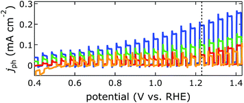
Enhanced PEC performance (Fig. 4) was observed for BiVO4 with smallest crystallite areas, smallest L and smallest surface Bi/V ratio of 1.1; this material was made with an [I−]/[Bi3+] ratio of 8 in the electrodeposition bath. Photocurrent generation at 1.23 V vs. RHE was increased by a factor of 5, compared to the material prepared without NaI in the plating bath, which exhibited a Bi-rich surface (Bi/V ratio 2.9) and larger crystallites. Photoanodes prepared with an [I−]/[Bi3+] ratio of 4 had the largest crystallites but only a Bi/V ratio of 1.5; the lower Bi-content at the surface apparently led to higher photocurrents.
With the goal to prepare BiVO4 films on FTO-glass with smaller crystallite sizes than obtainable by anodic electrodeposition, we turned to spin coating. We used two different precursor solutions: one followed a procedure reported by Gamelin,31 and the other, as a modification of that, had 0.34 M PEG added to the solution. We hypothesized that addition of PEG would increase the precursor solution's viscosity and this way change film morphology. All other experimental conditions were kept virtually identical. For both precursor solutions, the number of spin-coating cycles was varied from 2 to 8.
XPS and XRD data (ESI†) confirmed that all spin-cast films consisted of monoclinic scheelite BiVO4. Elemental Bi, V, and O were present in survey XP spectra. High-resolution XP spectra of the Bi 4d and V 2p core level regions revealed that each spin–orbit split peak could be described by a single Gaussian–Lorentzian component, which suggests that Bi and V existed in single oxidation states. The binding energies and branching ratios were virtually the same as those found for electrodeposited films.
As shown in Fig. 5, the different preparation conditions led to notably different film morphologies, although only one experimental parameter was varied at a time. All spin-coated BiVO4 films exhibited smaller crystallite sizes than electrodeposited films.
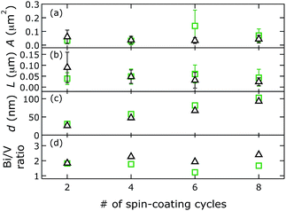
We quantified distributions of crystallite areas and aspect-ratio-normalised diameters, film thicknesses, and chemical surface compositions as described above (Fig. 6). Our spin-cast BiVO4 films exhibited smaller sizes than those prepared by electrodeposition. Mean crystallite areas A and mean aspect-ratio-normalised diameters L were on average smaller by a factor of 4.8 and 4.0, respectively. This suggests that aspect ratios were on average a factor of 1.8 higher in the spin cast materials.
Mean aspect-ratio-normalised diameters L were similar for spin-cast films made with PEG versus those made without PEG in the precursor solution with 2 and 4 spin-coating cycles, and larger for 6 and 8 cycles. Crystallite areas A did not follow a clear trend as a function of number of spin-coating cycles or depending on precursor solution. Perhaps not surprisingly, film thickness increased linearly with the number of spin-coating cycles for both precursor solutions. Films were on average 18% thicker when made from precursor solutions with higher viscosity. Surface Bi/V ratios of spin-cast BiVO4 films varied less across the different preparations but were higher than those for electrodeposited films. Surface Bi/V ratios of spin-cast BiVO4 made from precursor solutions without PEG were higher than those made from solutions with PEG.
We infer differences in metal salt solubility in the two precursor solvent mixtures (without and with PEG) to explain this last observation. We measured the solubilities of Bi(NO3)3·H2O and VO(C5H7O2)2 in the two precursor solvent mixtures (ESI†). We found that the solubility of VO(C5H7O2)2 was similar in both solvents. In contrast, Bi(NO3)3·5H2O was 2.5 times more soluble in the solution without PEG. We propose that, as a precursor solution droplet dries, some Bi(NO3)3·5H2O remains dissolved when all vanadium is already deposited. This leads to a higher surface Bi/V ratio.
Our electrodeposited and spin-cast BiVO4 on standard FTO-glass electrodes yielded photocurrents (at 1.23 V vs. RHE) that were comparable to those in Table S1.† In Fig. 7, they are depicted as a function of individual materials properties.
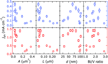 | ||
| Fig. 7 Effect of physical properties of electrodeposited (circles) and spin-cast (squares) BiVO4 on PEC performance, without (blue) and with (red) sulfite (ESI†) in the electrolyte. Photocurrents were measured at 1.23 V vs. RHE. | ||
Rough trends were only discernible from the properties L and d. Photocurrents were maximised at L ca. 0.05 μm and d ca. 65 nm; the optimal photocurrent density was 0.44 and 1.4 mA cm−2 in electrolytes without and with sulfite, respectively. This is similar to reported PEC performance.21,23,24,28,32,41–44 Our observed film thickness is likely the optimal trade-off between absorption (thicker is better) and majority carrier transport (thinner is better). No trend could be derived from the property A (see below). Photocurrents of our materials did not correlate with the surface Bi/V ratio, as would be expected based on previous work.17,23,41,45 Resistivities of BiVO4 films were measured to assess their effect on photocurrent generation; they were 4.4 × 10⁻⁵ and 8.7 × 10⁻⁵ Ω cm (with an error of 20%) for films made by spin coating and electrodeposition, respectively. Film conductivity cannot account for the differences in PEC performance we observed.
In materials the complex interplay of many properties matters. Therefore, we correlated photocurrents to morphology and surface composition simultaneously (Fig. 8). We observed clear trends from this analysis, which allowed for a better prediction of which combined properties led to improved performance. To the best of our knowledge, reported BiVO4 photocurrents have only been discussed to date as a function of individual properties, such as crystal phase,18,46 SEM image appearance,41 quantified particle size,46 thickness,23,24 and chemical composition.17,23,41,45 From our bivariate data analysis, we could differentiate which properties governed photocurrent generation.
We used A or L as y-axes in the bivariate PEC performance graphs to evaluate from which size parameter we could derive a trend. Photocurrents steadily increased as L decreased, but there was no clear dependence on A, suggesting that for our photoanodes charge separation efficiency was more important for PEC performance than interfacial characteristics between BiVO4 and FTO. Usually SEM images are analysed in terms of crystallite size, which is equivalent to our evaluation of area distributions A. We found, however, that the quantity L better captured dimensions that govern photocurrent generation, both in electrolytes with and without sulfite (ESI†). Crystallite area distributions inherently lack consideration of actual crystallite shape properties, such as aspect ratios. Therefore, we focused in the following on the quantity L to describe morphology. Hypothetically, L would be a better predictor of photocurrent generation than A only in thick films, where different orientations of grains give rise to different diffusion pathways within the films. Our data show that even in thin films, L is a better correlated to activity than A.
We compared electrodeposited materials with similar values for L, such as the BiVO4 films made without iodide and an [I−]/[Bi3+] ratio of 12. Their Bi/V ratios were found to be 2.9 and 1.1, respectively. Photoanodes with an almost stoichiometric Bi/V ratio outperformed those with Bi-rich surfaces. Ager also reported inferior performance for off-stoichiometric films but did not differentiate the effects of film morphology differences and surface compositions.23 Electrodeposited BiVO4 films with virtually the same chemical surface composition but smaller L produced higher photocurrents; the films made with an [I−]/[Bi3+] ratio of 8 surpassed those prepared from plating baths with an [I−]/[Bi3+] ratio of 12. Therefore, we conclude that unmodified, monoclinic scheelite BiVO4 photoanodes performed best with almost stoichiometric chemical surface compositions and smallest aspect-ratio-normalised diameters, which suggest that small crystallites with high aspect ratios were beneficial. These trends were found in both electrolytes, with and without sacrificial hole acceptor.
Because it is difficult to derive trends from four data points plotted in bivariate fashion, we focused on our spin-coated films. The potential for photocurrent generation was not equal among our spin-coating preparations. Variation of the number of spin-coating cycles and viscosity of the precursor solution produced BiVO4 films with different thicknesses; thicker BiVO4 layers absorbed more simulated sunlight. To account for this additional effect, we normalised photocurrent densities to the overlap integral J of a material's optical spectrum and the simulated sunlight spectrum for the following PEC performance evaluation (Fig. 9). This could be done because all electrodes were tested under virtually identical conditions.
The relative PEC performances of spin-cast BiVO4 photoanodes, normalised as described above, depended strongly on the intertwined effects of chemical surface composition and crystallite morphology in both electrolytes. Highest normalised photocurrents were obtained for L = (51 ± 9) nm and least Bi-rich surfaces. Like our electrodeposited BiVO4 films, materials with more Bi-rich surfaces (Bi/V ratio > 2) performed poorly, irrespective of L. Photoanodes with larger mean aspect-ratio-normalised diameters (L > 80 nm) were also inferior, more so in electrolyte without sacrificial hole acceptor. Adding sulfite to the electrolyte seemed to help electron–hole separation at the BiVO4–electrolyte interface, presumably because the reaction of holes with sulfite is faster than with water. Reduced PEC performance was obtained from materials with an L < 37 nm, likely because of mass transport limitations. We observed lower photocurrents relative to best performance in electrolytes with hole acceptor compared to those without, because mass transport is more critical in the faster oxidation reaction.
We have shown that intertwined material properties were responsible for optimised photocurrent generation of BiVO4 photoanodes. Morphology quantification in terms of aspect-ratio-normalised diameter, not just crystallite size, jointly with knowledge on the chemical surface composition was crucial to derive clear PEC performance trends. The interplay of several physical properties needed to be probed to understand the large variations in photocurrent generation of these complex metal oxide photoelectrodes.
Conclusions
We compared physical properties of bare, undoped monoclinic scheelite BiVO4 electrodes on FTO-glass without sublayers or co-catalysts with their PEC performance, to shed light on the reported large variations of photocurrents. Morphologies and chemical surface compositions of BiVO4 films, made by electrodeposition and spin coating, were very dependent on single experimental parameters.We devised an anodic electrodeposition procedure with different amounts of iodide added to the aqueous plating bath, to increase Bi ion solubility. This enabled us to prepare BiVO4 films with virtually identical thicknesses but different morphologies and to control surface Bi content. Smaller crystallites were obtained by spin coating, but thicknesses of spin-cast films linearly increased with the number of spin-coating cycles. To ensure comparability across films that absorbed different amounts of light, photocurrent densities of spin-cast films were normalised to the overlap integral of the films' optical spectrum and the simulated-sunlight spectrum.
We quantified morphologies from SEM images as distributions of crystallite areas and aspect-ratio-normalised diameters, surface Bi/V ratios were derived from XPS data. Correlation of photocurrents with individual material properties yielded only rough trends. We obtained clear trends from bivariate data, where photocurrent densities were plotted as a function of both chemical surface compositions and mean aspect-ratio-normalised diameters. A combination of near-stoichiometric surface compositions and mean aspect-ratio-normalised diameters, which were small enough for maximum charge separation yet large enough to prevent mass transport limitations, produced the best PEC performance.
Acknowledgements
We thank June Wicks for help with SEM imaging, Matthew Shaner for providing electrodeposited BiVO4 samples on FTO-glass prepared according to Choi,32 Richard P. Gerhart for fabrication of the photoelectrochemical cell, and Robert H. Coridan for valuable discussions. Research was performed at the Molecular Materials Research Center of the Beckman Institute of the California Institute of Technology. T.S.S. acknowledges a SURF Fellowship in honour of Dr Terry Cole, and B.M.H. is an NSF Graduate Fellow. This work was supported by the NSF CCI Solar Fuels Program (CHE-1305124) and the Arnold and Mabel Beckman Foundation.Notes and references
- H. B. Gray, Nat. Chem., 2009, 1, 7 CrossRef CAS PubMed.
- M. S. Prévot and K. Sivula, J. Phys. Chem. C, 2013, 117, 17879–17893 Search PubMed.
- K. Sivula, J. Phys. Chem. Lett., 2013, 4, 1624–1633 CrossRef CAS PubMed.
- A. Fujishima and K. Honda, Nature, 1972, 238, 37–38 CrossRef CAS PubMed.
- E. Borgarello, J. Kiwi, E. Pelizzetti, M. Visca and M. Grätzel, Nature, 1981, 289, 158–160 CrossRef CAS.
- A. J. Bard and M. A. Fox, Acc. Chem. Res., 1995, 28, 141–145 CrossRef CAS.
- N. S. Lewis and D. G. Nocera, Proc. Natl. Acad. Sci. U. S. A., 2006, 103, 15729–15735 CrossRef CAS PubMed.
- G. W. Crabtree and M. S. Dresselhaus, MRS Bull., 2008, 33, 421–428 CrossRef CAS.
- P. C. K. Vesborg and T. F. Jaramillo, RSC Adv., 2012, 2, 7933–7947 RSC.
- M. G. Walter, E. L. Warren, J. R. McKone, S. W. Boettcher, Q. Mi, E. A. Santori and N. S. Lewis, Chem. Rev., 2010, 110, 6446–6473 CrossRef CAS PubMed.
- J. R. McKone, N. S. Lewis and H. B. Gray, Chem. Mater., 2013, 26, 407–414 CrossRef.
- A. Harriman, I. J. Pickering, J. M. Thomas and P. A. Christensen, J. Chem. Soc., Faraday Trans. 1, 1988, 84, 2795–2806 RSC.
- M. Pourbaix, Atlas of Electrochemical Equilibria in Aqueous Solutions, Pergamon Press, New York, 1966 Search PubMed.
- S. Haussener, C. Xiang, J. M. Spurgeon, S. Ardo, N. S. Lewis and A. Z. Weber, Energy Environ. Sci., 2012, 5, 9922–9935 CAS.
- Y. Park, K. J. McDonald and K.-S. Choi, Chem. Soc. Rev., 2013, 42, 2321–2337 RSC.
- F. F. Abdi, N. Firet, A. Dabirian and R. van de Krol, MRS Online Proc. Libr., 2012, 1446, 7–12 Search PubMed.
- A. Kudo, K. Omori and H. Kato, J. Am. Chem. Soc., 1999, 121, 11459–11467 CrossRef CAS.
- S. Tokunaga, H. Kato and A. Kudo, Chem. Mater., 2001, 13, 4624–4628 CrossRef CAS.
- A. Walsh, Y. Yan, M. N. Huda, M. M. Al-Jassim and S.-H. Wei, Chem. Mater., 2009, 21, 547–551 CrossRef CAS.
- A. Kudo, K. Ueda, H. Kato and I. Mikami, Catal. Lett., 1998, 53, 229–230 CrossRef CAS.
- H. W. Jeong, T. H. Jeon, J. S. Jang, W. Choi and H. Park, J. Phys. Chem. C, 2013, 117, 9104–9112 CAS.
- A. J. E. Rettie, H. C. Lee, L. G. Marshall, J.-F. Lin, C. Capan, J. Lindemuth, J. S. McCloy, J. Zhou, A. J. Bard and C. B. Mullins, J. Am. Chem. Soc., 2013, 135, 11389–11396 CrossRef CAS PubMed.
- L. Chen, E. Alarcón-Lladó, M. Hettick, I. D. Sharp, Y. Lin, A. Javey and J. W. Ager, J. Phys. Chem. C, 2013, 117, 21635–21642 CAS.
- F. F. Abdi, N. Firet and R. van de Krol, ChemCatChem, 2013, 5, 490–496 CrossRef CAS.
- S. K. Cho, H. S. Park, H. C. Lee, K. M. Nam and A. J. Bard, J. Phys. Chem. C, 2013, 117, 23048–23056 CAS.
- G. Wang, Y. Ling, X. Lu, F. Qian, Y. Tong, J. Z. Zhang, V. Lordi, C. Rocha Leao and Y. Li, J. Phys. Chem. C, 2013, 117, 10957–10964 CAS.
- Y. H. Ng, A. Iwase, A. Kudo and R. Amal, J. Phys. Chem. Lett., 2010, 1, 2607–2612 CrossRef CAS.
- E. Alarcon-Llado, L. Chen, M. Hettick, N. Mashouf, Y. Lin, A. Javey and J. W. Ager, Phys. Chem. Chem. Phys., 2014, 16, 1651–1657 RSC.
- Y. Liang, T. Tsubota, L. P. A. Mooij and R. van de Krol, J. Phys. Chem. C, 2011, 115, 17594–17598 CAS.
- F. F. Abdi, L. Han, A. H. M. Smets, M. Zeman, B. Dam and R. van de Krol, Nat. Commun., 2013, 4, 2195–2201 Search PubMed.
- D. K. Zhong, S. Choi and D. R. Gamelin, J. Am. Chem. Soc., 2011, 133, 18370–18377 CrossRef CAS PubMed.
- J. A. Seabold and K.-S. Choi, J. Am. Chem. Soc., 2012, 134, 2186–2192 CrossRef CAS PubMed.
- E. Yablonovitch, J. Opt. Soc. Am., 1982, 72, 899–907 CrossRef.
- D. M. Callahan, J. N. Munday and H. A. Atwater, Nano Lett., 2011, 12, 214–218 CrossRef PubMed.
- F. C. Zumsteg, NBS Spec. Publ. (U. S.), 1980, 574, 156–159 CAS.
- K. J. McDonald and K.-S. Choi, Energy Environ. Sci., 2012, 5, 8553–8557 CAS.
- X-ray Photoelectron Spectroscopy Database 20, Version 4.1, National Institute of Standards and Technology, Gaithersburg, 2012, http://srdata.nist.gov/xps/ Search PubMed.
- Y. Schuhl, H. Baussart, R. Delobel, M. Le Bras, J.-M. Leroy, L. Gengembre and J. Grimblot, J. Chem. Soc., Faraday Trans. 1, 1983, 79, 2055–2069 RSC.
- J. Su, X.-X. Zou, G.-D. Li, X. Wei, C. Yan, Y.-N. Wang, J. Zhao, L.-J. Zhou and J.-S. Chen, J. Phys. Chem. C, 2011, 115, 8064–8071 CAS.
- D. A. Shirley, Phys. Rev. B: Condens. Matter Mater. Phys., 1972, 5, 4709–4714 CrossRef.
- S. P. Berglund, D. W. Flaherty, N. T. Hahn, A. J. Bard and C. B. Mullins, J. Phys. Chem. C, 2011, 115, 3794–3802 CAS.
- S. K. Choi, W. Choi and H. Park, Phys. Chem. Chem. Phys., 2013, 15, 6499–6507 RSC.
- K. Sayama, N. Wang, Y. Miseki, H. Kusama, N. Onozawa-Komatsuzaki and H. Sugihara, Chem. Lett., 2010, 39, 17–19 CrossRef CAS.
- J. Su, L. Guo, S. Yoriya and C. A. Grimes, Cryst. Growth Des., 2009, 10, 856–861 Search PubMed.
- H. Ye, J. Lee, J. S. Jang and A. J. Bard, J. Phys. Chem. C, 2010, 114, 13322–13328 CAS.
- A. Iwase and A. Kudo, J. Mater. Chem., 2010, 20, 7536–7542 RSC.
Footnote |
| † Electronic supplementary information (ESI) available: Reported BiVO4 photoanode performances; experimental details; XPS and XRD data of BiVO4 on FTO-glass photoanodes; statistics of crystallite area distributions and aspect-ratio-normalised diameter distributions; optical spectra of BiVO4 on FTO-glass photoanodes; effect of iodide on the electrodeposition baths; solubility of metal salts in the spin-coating precursor solutions; bivariate data of electrodeposited BiVO4 without sulfite in the electrolyte; simulated sunlight spectrum; SEM images of FTO on glass and BiVO4 on FTO-glass. See DOI: 10.1039/c4mh00156g |
| This journal is © The Royal Society of Chemistry 2015 |

