Ambipolar charge transport of TIPS-pentacene single-crystals grown from non-polar solvents†
Guobiao
Xue
a,
Congcheng
Fan
a,
Jiake
Wu
a,
Shuang
Liu
a,
Yujing
Liu
ab,
Hongzheng
Chen
a,
Huolin L.
Xin
b and
Hanying
Li
*a
aMOE Key Laboratory of Macromolecule Synthesis and Functionalization, State Key Laboratory of Silicon Materials, Department of Polymer Science and Engineering, Zhejiang University, Hangzhou, 310027, P. R. China. E-mail: hanying_li@zju.edu.cn
bCenter for Functional Nanomaterials, Brookhaven National Laboratory, Upton, NY 11973, USA
First published on 21st January 2015
Abstract
Charge transport of solution-grown TIPS-pentacene single-crystals depends on the polarity of the used solvents. Crystals grown from non-polar solvents exhibit ambipolar transport (μe 0.020 cm2 V−1 s−1; μh 5.0 cm2 V−1 s−1), while polar solvents suppress electron transport. This work indicates that appropriate selection of solvents should further harvest the n-type behaviors of organic semiconductors.
Conceptual insightsAmbipolar organic field-effect transistors (OFETs) are essential for various electronic applications such as organic complementary circuits and light-emitting transistors. Although organic semiconductors should, in principle, provide an equal opportunity for both holes and electrons, electron transport is practically less-frequently observed. Currently, it is widely believed that the limited electron transport is associated with high electron injection barriers and the electron traps at the semiconductor–dielectric interface. Here, we demonstrate an ignored alternative source to suppress the electron transport. We show that trace amounts of polar solvent residues from crystal growth of organic semiconductors ruin n-channel conductance. In contrast, the non-polar solvents do not. Grown from various non-polar solvents, single-crystals of 6,13-bis(triisopropyl-silylethynyl)pentacene (TIPS-pentacene), a standard p-channel material, conduct electrons in FETs using Au as both source and drain electrodes. As hexane was used, we achieved an electron mobility as high as 0.020 cm2 V−1 s−1 as well as a hole mobility of 5.0 cm2 V−1 s−1. Hence, this work should further harvest the n-type behaviors of organic semiconductors. |
Organic field-effect transistors (OFETs) are promising for a variety of low-cost, light-weight and flexible electronic applications.1,2 Specifically, ambipolar OFETs in which both holes and electrons are mobile have been attracting increasing attention for their applications in light-emitting transistors3–6 and complementary circuits.7–11 Fundamentally, organic semiconductors should allow both holes and electrons to transport.11–14 But in practice, unipolar transport dominates. Initially, ambipolar OFETs were realized by combining the electronic functions of both p- and n-channel components in the active layers in the forms of bi-layers,15–18 blends19,20 and co-crystals.21–24 Although it is difficult to achieve ambipolar transport from single-component active layers mainly due to the lack of electron conductance,14,25,26 a few examples were, subsequently, proved to conduct both holes and electrons.11 The obstacles to electron conductance have been found to be associated with high electron injection barriers3,14 and the electron traps at the semiconductor–dielectric interface.13 By reducing the electron injection barrier using either narrow band-gap semiconductors10,11,27,28 or low work-function electrodes,9,29–33 ambipolar OFETs were greatly developed. Furthermore, eliminating the electron traps (such as hydroxyl groups) on the dielectrics resulted in the harvest of n-type behaviors.3,12,13,25,34 Currently, OFETs with the highest mobilities are fabricated from a low-band gap polymer with a hole mobility of 8.84 cm2 V−1 s−1 and an electron mobility of 4.34 cm2 V−1 s−1.28 The progress of ambipolar OFETs highlights the effects of the electrode/semiconductor and semiconductor/dielectric interfaces on the charge transport. However, we envision that another possible source to reduce electron transport induced during device fabrication might be neglected. Solution processing35–38 and solvent annealing39,40 are widely used to fabricate high-performance OFETs and solvent residues are inevitably introduced to the semiconducting layers. These solvent molecules might potentially affect the charge transport. In this work, FETs were fabricated based on single-crystals of 6,13-bis(triisopropyl-silylethynyl)pentacene (TIPS-pentacene)41 grown from a variety of solvents to examine solvent effects on the device performance. We found that, for this widely recognized p-channel material,42–47 ambipolar transport in FETs using Au as both source and drain electrodes could be realized as various non-polar solvents were used.
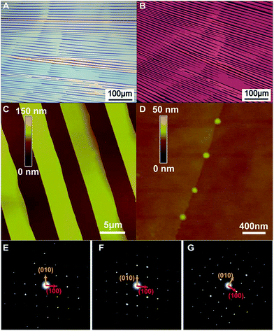
TIPS-pentacene is soluble in various solvents,41 and thus was selected in this work to study the solvent effect. Single-crystals of TIPS-pentacene were prepared from six solvents including hexane, heptane, cyclohexane, dichloromethane (CH2Cl2), trichloromethane (CHCl3) and tetrahydrofuran (THF), using the droplet-pinned crystallization (DPC) method.48,49 Divinyltetramethyldisiloxane-bis(benzocyclobutene) (BCB)-covered SiO2/Si substrates were used to grow the crystals as BCB was found to efficiently eliminate the electron traps arising from the surface hydroxyl group on SiO2.13 In all cases, well-aligned single-crystals were obtained, as shown by the optical microscopy (OM) images with crossed polarizers (Fig. 1A and B and S1†). The single-crystallinity was reconfirmed by selected-area electron diffraction (SAED) patterns. Similar SAED patterns with single sets of diffraction spots were found in the crystals from all the six solvents (Fig. 1E–G), indicative of the same crystallographic structure. The millimeter-long ribbon shaped crystals were 35–173 nm high and 3.3–43 μm wide. Steps were observed on the flat terraces (Fig. 1C and D), with a step height of 1.63 nm that is close to 1.65 nm of the (001) d-spacing. Nanoparticles, likely from impurities expelled by the growing crystals,50 were found on the crystal surfaces, especially at the step edges (Fig. 1D). With these well-aligned crystals, FETs were constructed by depositing Au source and drain electrodes in a top-contact, bottom-gate configuration (Fig. 2C, inset), with a channel length (L) of 50 μm and width (W) of 1 mm. The charge transport characteristics were investigated in a N2 atmosphere and the saturation regime mobility was calculated. As the crystals did not cover the whole channel region, the real W/L value was measured (Fig. 2F, inset) to calculate the mobility values.
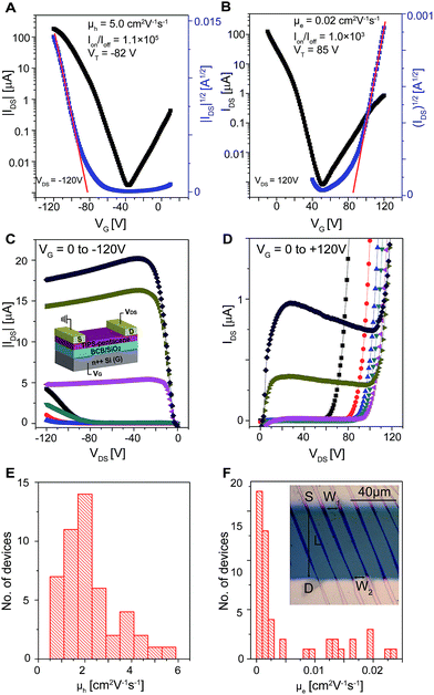
We first examined the FETs based on crystals grown from hexane. The typical transfer and output characteristics are shown in Fig. 2A–D, wherein ambipolar behavior is surprisingly observed. The typical output characteristics in both p-channel (Fig. 2C) and n-channel (Fig. 2D) operation modes exhibited excellent gate modulation. Histograms of both hole and electron mobility for 50 devices from 3 substrates are shown in Fig. 2E and F. For the hole transport, an average hole mobility (μh) of 2.2 ± 1.2 cm2 V−1 s−1 (range: 0.41 to 5.4 cm2 V−1 s−1, Fig. 2E), on-to-off current ratios (Ion/Ioff) > 103, and threshold voltages (VT) between −66 and −87 V were obtained. For the electron transport, an average electron mobility (μe) of 5.3 × 10⁻³ ± 7.2 × 10⁻³ cm2 V−1 s−1 (range: 5.5 × 10⁻⁵ to 2.4 × 10⁻² cm2 V−1 s−1, Fig. 2F), Ion/Ioff > 6, and VT between 44 and 92 V were achieved. The large VT is similar to the previous reports on ambipolar OFETs10,28,29,33 and suggests the existence of traps. The variations of μ and VT are mainly associated with two factors: first, the varied crystal thickness and width that will induce different contact resistances; second, the slightly different orientation of the crystals with respect to the electrodes that leads to anisotropic transport. For a single device, mobilities of 5.0 cm2 V−1 s−1 for hole transport and 0.020 cm2 V−1 s−1 for electron transport were obtained. The hole mobility obtained here is among the highest values for unstrained TIPS-pentacene crystals,42,44,50,51 while the electron transport has not been previously observed as Au is used as both source and drain electrodes. This observation is obviously different from the n-channel behavior reported before where the crystals were interfaced with a low-work-function metal electrode.52 One possible explanation for this unprecedented electron transport is that the TIPS-pentacene crystals might be n-doped by unknown impurities (e.g., from solvent, chemical or substrate).52–54 However, as n-doped,52 the crystals exhibited electron transport but their hole transport was suppressed remarkably. The emergence of the electron transport with a concomitant unsuppressed hole mobility in the current work implies a different mechanism that is further studied below.
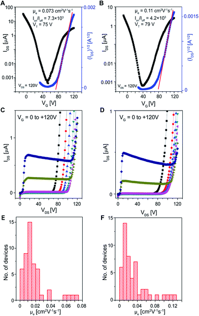
Another possible explanation for the electron transport in hexane-grown crystals is solvent polarity. Polar molecules were previously shown to interfere with the charge transport,55–58 while the non-polar ones were not.44,56,59 We hypothesized that the non-polar nature of hexane was associated with the emergence of electron transport. Accordingly, we examined two more non-polar solvents and three polar solvents. 50 devices based on crystals grown from heptane, a non-polar solvent, were studied in the n-channel operation mode. Clear electron transport was observed from both the transfer and output characteristics (Fig. 3A and C). A μe of 1.8 × 10⁻² ± 1.6 × 10⁻² cm2 V−1 s−1 (range: 4.0 × 10⁻⁴ to 7.3 × 10⁻² cm2 V−1 s−1, Fig. 3E), Ion/Ioff > 10, and VT between 64 and 90 V were obtained. Similarly, FETs based on crystals grown from cyclohexane, also a non-polar solvent, exhibited electron transport (Fig. 3B and D). A μe of 3.2 × 10⁻² ± 2.9 × 10⁻² cm2 V−1 s−1 (range: 3.3 × 10⁻³ to 1.3 × 10⁻¹ cm2 V−1 s−1, Fig. 3F), Ion/Ioff > 10, and VT between 53 and 90 V were obtained, as summarized in Table 1. In addition to the electron transport, these devices still maintained their hole transport properties (Fig. S2 and S3†).
 | ||
| Fig. 3 FET characteristics of the crystals grown from heptane (A, C and E) or cyclohexane (B, D and F) solutions. (A–D) Typical transfer (A and B) and output characteristics (C and D) of the FETs in the n-channel operation mode. (E and F) Histograms of the μe of 50 FETs. Typical transfer, output characteristics in the p-channel operation mode and histograms of the μh of these FETs are shown in Fig. S2 and S3.† | ||
| Solvents | μ e (cm2 V−1 s−1) | I on/Ioff | V T (V) | |
|---|---|---|---|---|
| Average | Max | |||
| a Measured in a glovebox. As the devices were exposed to air, the electron transport behavior disappeared because the electrons were trapped by oxygen and moisture. | ||||
| Hexane | 5.3 × 10⁻³ ± 7.2 × 10⁻³ | 2.4 × 10⁻² | >6 | 44 to 92 |
| Heptane | 1.8 × 10⁻² ± 1.6 × 10⁻² | 7.3 × 10⁻² | >10 | 64 to 90 |
| Cyclohexane | 3.2 × 10⁻² ± 2.9 × 10⁻² | 1.3 × 10⁻¹ | >10 | 53 to 90 |
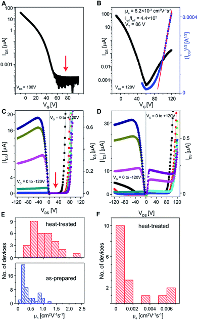
In sharp contrast to the three non-polar solvents, FETs based on the crystals grown from CH2Cl2, a polar solvent, showed no gate modulation in the n-channel operation mode (Fig. 4A and C, arrows). Similarly, crystals grown from the other two polar solvents, CHCl3 and THF, exhibited no electron transport properties except that a very small number of devices (3 out of 50 devices) for the CHCl3-grown crystals showed an electron mobility of ∼1.0 × 10⁻³ cm2 V−1 s−1. As expected, these devices still worked in the p-channel operation mode (Fig. 4A, C and E and S4†). The distinct electron transport properties of the crystals grown from the six solvents indicate a significant solvent effect on charge transport. Clearly, electron transport in the crystals grown from polar solvents is suppressed. Because the same device configuration and the same semiconducting layer were used, the solvent effect should have originated from the solvent molecules themselves. We believe that the solvents affect the charge transport through their trace amount of residues in the crystal or at the crystal/substrate interface. Random electric fields associated with the residual polar solvent molecules introduce energetic disorder and positional disorder55 in the TIPS-pentacene crystals and reduce their charge transport performance. The negative effect of polar molecules on p-channel FETs was observed previously56,60 and was not appreciated for n-channel FETs. In order to prove the existence of the trace amount of solvents, we compared the FET performance between the as-prepared and heat-treated CH2Cl2-grown crystals. 31 devices were heated and tested after cooling down. More than half (17 out of 31) of the devices exhibited electron transport with the highest μe of 6.3 × 10⁻³ cm2 V−1 s−1 (Fig. 4F). For a single device, their transfer and output characteristics before and after heat treatment clearly indicated a transition from an electron inactive channel to an electron transporting channel (Fig. 4A–D). In addition to the emergence of electron transport, the hole mobility increased for each heated device (Fig. 4E). Also, instead of heat treatment, keeping in a glovebox at room temperature for a week also provided the devices with originally non-existent electron transport ability. Because the heat treatment did not change the molecular arrangement in the crystals as shown by SAED patterns (Fig. 1F and G), the emergence of electron transport is attributed to the partial removal of polar solvent residues during heating or lastingly staying, and indirectly proves the existence of the trace amount of solvent molecules. In addition, the crystals were grown from mixed solvents of hexane and CH2Cl2 in different volume ratios. The electron transport was found to be gradually suppressed as the concentration of CH2Cl2 increased consistently with the proposed negative effect of polar solvent residues on the electron transport (Fig. S5†).
Conclusions
In summary, we demonstrated a solvent effect on the electron transport properties of TIPS-pentacene. As grown from non-polar solvents including hexane, heptane and cyclohexane, TIPS-pentacene crystals exhibited electron transport with an electron mobility up to 0.13 cm2 V−1 s−1 in addition to hole transport. In contrast, the crystals grown from polar solvents (CH2Cl2, CHCl3, THF) showed only hole transport except that a very small number (3 out of 150) of devices exhibited electron transport (mobility ∼ 1.0 × 10⁻³ cm2 V−1 s−1). This discrepancy between polar and non-polar solvents suggests a dipolar effect of the residual solvents in the crystals on their charge transport. As such, this work provides an alternative source for charge transport reduction. Together with the widely used strategies to promote electron transport including reducing the charge injection barrier3 and eliminating the charge trapping,13 appropriate selection of solvents and/or additives should further harvest the electron behaviors of solution-grown organic thin films and crystals.Acknowledgements
This work was supported by the 973 Program (2014CB643503), National Natural Science Foundation of China (51222302, 51373150, 51461165301, 91233114), Zhejiang Province Natural Science Foundation (LZ13E030002), and Fundamental Research Funds for the Central Universities. HLX is supported by the Center for Functional Nanomaterials, Brookhaven National Laboratory, which is supported by the U.S. Department of Energy, Office of Basic Energy Sciences, under Contract no. DE-AC02-98CH10886. YJL thanks China Scholarship Council (CSC) for financial support.Notes and references
- H. Sirringhaus, Adv. Mater., 2014, 26, 1319 CrossRef CAS PubMed.
- H. L. Dong, X. L. Fu, J. Liu, Z. R. Wang and W. P. Hu, Adv. Mater., 2013, 25, 6158 CrossRef CAS PubMed.
- J. Zaumseil and H. Sirringhaus, Chem. Rev., 2007, 107, 1296 CrossRef CAS PubMed.
- J. Zaumseil, R. H. Friend and H. Sirringhaus, Nat. Mater., 2006, 5, 69 CrossRef CAS.
- H. Nakanotani, M. Saito, H. Nakamura and C. Adachi, Adv. Funct. Mater., 2010, 20, 1610 CrossRef CAS.
- X. J. Li, Y. X. Xu, F. Li and Y. G. Ma, Org. Electron., 2012, 13, 762 CrossRef CAS PubMed.
- B. Crone, A. Dodabalapur, Y. Y. Lin, R. W. Filas, Z. N. Bao, A. LaDuca, R. Sarpeshkar, H. E. Katz and W. Li, Nature, 2000, 403, 521 CrossRef CAS PubMed.
- T. D. Anthopoulos, Appl. Phys. Lett., 2007, 91, 113513 CrossRef PubMed.
- T. Uemura, M. Yamagishi, Y. Okada, K. Nakayama, M. Yoshizumi, M. Uno and J. Takeya, Adv. Mater., 2010, 22, 3938 CrossRef CAS PubMed.
- J. Lee, A. R. Han, J. Kim, Y. Kim, J. H. Oh and C. Yang, J. Am. Chem. Soc., 2012, 134, 20713 CrossRef CAS PubMed.
- E. J. Meijer, D. M. de Leeuw, S. Setayesh, E. van Veenendaal, B. H. Huisman, P. W. M. Blom, J. C. Hummelen, U. Scherf, J. Kadam and T. M. Klapwijk, Nat. Mater., 2003, 2, 679 CrossRef PubMed.
- S. Z. Bisri, C. Piliego, J. Gao and M. A. Loi, Adv. Mater., 2014, 26, 1176 CrossRef CAS PubMed.
- L. L. Chua, J. Zaumseil, J. F. Chang, E. C. W. Ou, P. K. H. Ho, H. Sirringhaus and R. H. Friend, Nature, 2005, 434, 194 CrossRef CAS PubMed.
- H. Sirringhaus, Nat. Mater., 2003, 2, 641 CAS.
- C. C. Fan, A. P. Zoombelt, H. Jiang, W. F. Fu, J. K. Wu, W. T. Yuan, Y. Wang, H. Y. Li, H. Z. Chen and Z. N. Bao, Adv. Mater., 2013, 25, 5762 CrossRef CAS PubMed.
- Y. J. Zhang, H. L. Dong, Q. X. Tang, S. Ferdous, F. Liu, S. C. B. Mannsfeld, W. P. Hu and A. L. Briseno, J. Am. Chem. Soc., 2010, 132, 11580 CrossRef CAS PubMed.
- J. Wang, H. B. Wang, X. J. Yan, H. C. Huang and D. H. Yan, Appl. Phys. Lett., 2005, 87, 093507 CrossRef PubMed.
- A. Dodabalapur, H. E. Katz, L. Torsi and R. C. Haddon, Science, 1995, 269, 1560 CAS.
- C. Rost, S. Karg, W. Riess, M. A. Loi, M. Murgia and M. Muccini, Appl. Phys. Lett., 2004, 85, 1613 CrossRef CAS PubMed.
- J. Wang, H. B. Wang, X. J. Yan, H. C. Huang, D. Jin, J. W. Shi, Y. H. Tang and D. H. Yan, Adv. Funct. Mater., 2006, 16, 824 CrossRef CAS.
- S. K. Park, S. Varghese, J. H. Kim, S. J. Yoon, O. K. Kwon, B. K. An, J. Gierschner and S. Y. Park, J. Am. Chem. Soc., 2013, 135, 4757 CrossRef CAS PubMed.
- T. Wakahara, P. D'Angelo, K. Miyazawa, Y. Nemoto, O. Ito, N. Tanigaki, D. D. C. Bradley and T. D. Anthopoulos, J. Am. Chem. Soc., 2012, 134, 7204 CrossRef CAS PubMed.
- T. Hasegawa, K. Mattenberger, J. Takeya and B. Batlogg, Phys. Rev. B: Condens. Matter Mater. Phys., 2004, 69, 245115 CrossRef.
- Y. K. Qin, J. Zhang, X. Y. Zheng, H. Geng, G. Y. Zhao, W. Xu, W. P. Hu, Z. G. Shuai and D. B. Zhu, Adv. Mater., 2014, 26, 4093 CrossRef CAS PubMed.
- J. E. Anthony, A. Facchetti, M. Heeney, S. R. Marder and X. W. Zhan, Adv. Mater., 2010, 22, 3876 CrossRef CAS PubMed.
- Y. Zhao, Y. L. Guo and Y. Q. Liu, Adv. Mater., 2013, 25, 5372 CrossRef CAS PubMed.
- J. C. Bijleveld, A. P. Zoombelt, S. G. J. Mathijssen, M. M. Wienk, M. Turbiez, D. M. de Leeuw and R. A. J. Janssen, J. Am. Chem. Soc., 2009, 131, 16616 CrossRef CAS PubMed.
- J. Lee, A. R. Han, H. Yu, T. J. Shin, C. Yang and J. H. Oh, J. Am. Chem. Soc., 2013, 135, 9540 CrossRef CAS PubMed.
- T. Takahashi, T. Takenobu, J. Takeya and Y. Iwasa, Appl. Phys. Lett., 2006, 88, 033505 CrossRef PubMed.
- F. Cicoira, C. M. Aguirre and R. Martel, ACS Nano, 2011, 5, 283 CrossRef CAS PubMed.
- M. C. Gwinner, F. Jakubka, F. Gannott, H. Sirringhaus and J. Zaumseil, ACS Nano, 2012, 6, 539 CrossRef CAS PubMed.
- W. Xie, P. L. Prabhumirashi, Y. Nakayama, K. A. McGarry, M. L. Geier, Y. Uragami, K. Mase, C. J. Douglas, H. Ishii, M. C. Hersam and C. D. Frisbie, ACS Nano, 2013, 7, 10245 CrossRef CAS PubMed.
- T. Takahashi, T. Takenobu, J. Takeya and Y. Iwasa, Adv. Funct. Mater., 2007, 17, 1623 CrossRef CAS.
- Y. G. Wen and Y. Q. Liu, Adv. Mater., 2010, 22, 1331 CrossRef CAS PubMed.
- Y. B. Yuan, G. Giri, A. L. Ayzner, A. P. Zoombelt, S. C. B. Mannsfeld, J. H. Chen, D. Nordlund, M. F. Toney, J. S. Huang and Z. N. Bao, Nat. Commun., 2014, 5, 3005 Search PubMed.
- H. Minemawari, T. Yamada, H. Matsui, J. Tsutsumi, S. Haas, R. Chiba, R. Kumai and T. Hasegawa, Nature, 2011, 475, 364 CrossRef CAS PubMed.
- D. Q. Liu, X. M. Xu, Y. R. Su, Z. K. He, J. B. Xu and Q. Miao, Angew. Chem., Int. Ed., 2013, 52, 6222 CrossRef CAS PubMed.
- S. Allard, M. Forster, B. Souharce, H. Thiem and U. Scherf, Angew. Chem., Int. Ed., 2008, 47, 4070 CrossRef CAS PubMed.
- D. J. Mascaro, M. E. Thompson, H. I. Smith and V. Bulovic, Org. Electron., 2005, 6, 211 CrossRef CAS PubMed.
- K. C. Dickey, J. E. Anthony and Y. L. Loo, Adv. Mater., 2006, 18, 1721 CrossRef CAS.
- J. E. Anthony, J. S. Brooks, D. L. Eaton and S. R. Parkin, J. Am. Chem. Soc., 2001, 123, 9482 CrossRef CAS.
- M. M. Payne, S. R. Parkin, J. E. Anthony, C. C. Kuo and T. N. Jackson, J. Am. Chem. Soc., 2005, 127, 4986 CrossRef CAS PubMed.
- D. H. Kim, D. Y. Lee, H. S. Lee, W. H. Lee, Y. H. Kim, J. I. Han and K. Cho, Adv. Mater., 2007, 19, 678 CrossRef CAS.
- R. Hamilton, J. Smith, S. Ogier, M. Heeney, J. E. Anthony, I. McCulloch, J. Veres, D. D. C. Bradley and T. D. Anthopoulos, Adv. Mater., 2009, 21, 1166 CrossRef CAS.
- G. Giri, E. Verploegen, S. C. B. Mannsfeld, S. Atahan-Evrenk, D. H. Kim, S. Y. Lee, H. A. Becerril, A. Aspuru-Guzik, M. F. Toney and Z. N. Bao, Nature, 2011, 480, 504 CrossRef CAS PubMed.
- Y. Diao, B. C. K. Tee, G. Giri, J. Xu, D. H. Kim, H. A. Becerril, R. M. Stoltenberg, T. H. Lee, G. Xue, S. C. B. Mannsfeld and Z. N. Bao, Nat. Mater., 2013, 12, 665 CrossRef CAS PubMed.
- J. P. Hong and S. Lee, Angew. Chem., Int. Ed., 2009, 48, 3096 CrossRef CAS PubMed.
- H. Y. Li, B. C. K. Tee, J. J. Cha, Y. Cui, J. W. Chung, S. Y. Lee and Z. N. Bao, J. Am. Chem. Soc., 2012, 134, 2760 CrossRef CAS PubMed.
- H. Y. Li, C. C. Fan, M. Vosgueritchian, B. C. K. Tee and H. Z. Chen, J. Mater. Chem. C, 2014, 2, 3617 RSC.
- H. Y. Li, B. C. K. Tee, G. Giri, J. W. Chung, S. Y. Lee and Z. N. Bao, Adv. Mater., 2012, 24, 2588 CrossRef CAS PubMed.
- S. K. Park, T. N. Jackson, J. E. Anthony and D. A. Mourey, Appl. Phys. Lett., 2007, 91, 063514 CrossRef PubMed.
- B. D. Naab, S. Himmelberger, Y. Diao, K. Vandewal, P. Wei, B. Lussem, A. Salleo and Z. N. Bao, Adv. Mater., 2013, 25, 4663 CrossRef CAS PubMed.
- C. Z. Li, C. C. Chueh, H. L. Yip, F. Z. Ding, X. S. Li and A. K. Y. Jen, Adv. Mater., 2013, 25, 2457 CrossRef CAS PubMed.
- B. Lussem, M. L. Tietze, H. Kleemann, C. Hossbach, J. W. Bartha, A. Zakhidov and K. Leo, Nat. Commun., 2013, 4, 2775 Search PubMed.
- P. M. Borsenberger and H. Bassler, J. Chem. Phys., 1991, 95, 5327 CrossRef CAS PubMed.
- A. Babel and S. A. Jenekhe, Macromolecules, 2004, 37, 9835 CrossRef CAS.
- N. G. Martinelli, M. Savini, L. Muccioli, Y. Olivier, F. Castet, C. Zannoni, D. Beljonne and J. Cornil, Adv. Funct. Mater., 2009, 19, 3254 CrossRef CAS.
- F. Gholamrezaie, A. M. Andringa, W. S. C. Roelofs, A. Neuhold, M. Kemerink, P. W. M. Blom and D. M. de Leeuw, Small, 2012, 8, 241 CrossRef CAS PubMed.
- L. Fang, Y. Zhou, Y. X. Yao, Y. Diao, W. Y. Lee, A. L. Appleton, R. Allen, J. Reinspach, S. C. B. Mannsfeld and Z. N. Bao, Chem. Mater., 2013, 25, 4874 CrossRef CAS.
- J. Takeya, T. Nishikawa, T. Takenobu, S. Kobayashi, Y. Iwasa, T. Mitani, C. Goldmann, C. Krellner and B. Batlogg, Appl. Phys. Lett., 2004, 85, 5078 CrossRef CAS PubMed.
Footnote |
| † Electronic supplementary information (ESI) available. See DOI: 10.1039/c4mh00211c |
| This journal is © The Royal Society of Chemistry 2015 |


