
Origin of photoluminescence from colloidal gallium phosphide nanocrystals synthesized via a hot-injection method†
Sungwoo Kim‡
ad,
Kangha Lee‡b,
Sejin Kima,
O.-Pil Kwona,
Jin Hyuk Heoc,
Sang Hyuk Imc,
Sohee Jeongd,
Doh C. Lee*b and
Sang-Wook Kim*a
aDepartment of Molecular Science and Technology, Ajou University, Suwon 443-749, Republic of Korea. E-mail: swkim@ajou.ac.kr
bDepartment of Chemical and Biomolecular Engineering, KAIST Institute for the Nanocentury (KINC), Korea Advanced Institute of Science and Technology (KAIST), Daejeon 305-701, Republic of Korea. E-mail: dclee@kaist.edu
cDepartment of Chemical Engineering, College of Engineering, Kyung Hee University, 1 Seochon-dong, Giheung-gu, Yongin-si, Gyeonggi-do 446-701, Republic of Korea
dNanomechanical Systems Research Division, Korea Institute of Machinery and Materials, Daejeon 305-343, Republic of Korea
First published on 1st December 2014
Abstract
In this work, photoluminescence from colloidal GaP nanocrystals (NCs) synthesized via a hot-injection method is observed and analyzed. The emission and excitation spectra of the GaP NCs indicate that two transitions, near the direct and indirect bandgaps of bulk GaP, are responsible for the luminescence.
Semiconductor nanocrystals (NCs) of size comparable to or smaller than their characteristic electron–hole spacing, or quantum dots (QDs), exhibit a size-dependent energy gap and discrete energy levels due to quantum confinement effect. Narrow emission peaks and controlled exciton–exciton interactions render colloidal QDs best suited for various applications, such as photodetectors.1–4,12–14 Implementation of QDs in commercially available devices would require the use of toxicologically benign semiconductors. This obvious demand has spurred the search of cadmium-free alternative for prevalently studied cadmium chalcogenide QDs. While the list of Cd-free QDs includes InP, InAs, GaAs, and CuInS2,5–11 GaP is considered as a promising candidate for a blue fluorophore. However, GaP is an indirect bandgap semiconductor, thus non-emitting in bulk. One way to make GaP relevant as a light-emitting compound is to alleviate the indirect nature of the band structure via quantum confinement effect. In fact, several approaches have targeted the synthesis of GaP NCs in a strong quantum confinement regime: examples include dehalosilylation reaction,15,16 thermal decomposition of single-molecule precursors,17,18 and a relatively mild arrested precipitation method.19 Despite the considerable progress made by the community, the synthetic protocols reported thus far give rise to GaP NCs only with broad size distribution. Several attempts to produce more uniform-sized GaP NCs also highlighted the progress from the synthesis perspective. An important agenda in the mission of synthesizing monodisperse GaP NCs is to control the nucleation and growth of the colloidal particles. For example, some approaches exploited mild conditions in solution to slow down growth,20,22 while Lauth et al.21 used transmetalation reaction to speed up the nucleation. Whereas the development enabled more uniform GaP NCs in general, the studies often lack thorough analysis on their optical properties, such as photoluminescence (PL) and absorption. Rather, the controversy over the origin of the emission has heated, as GaP is a non-emitting, indirect-bandgap semiconductor in bulk. Therefore, developing growth of colloidal GaP NCs with a narrow size distribution has been called for.
In this communication, we report a simple synthetic method of colloidal GaP NCs and investigation of optical transitions by photoluminescence excitation (PLE) spectroscopy and PL decay dynamics analysis. GaP NCs integrated in a photodiode were tested for their ultraviolet (UV) response.
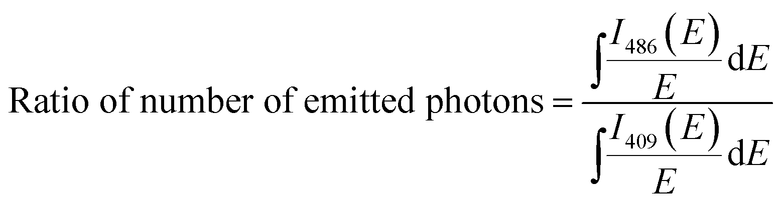
Colloidal GaP NCs were synthesized via a hot injection approach: gallium chloride (GaCl3) and tris(trimethylsilyl)phosphine ((TMS)3P) were injected into a mixture containing 1-octadecene (ODE) and palmitic acid (PA) in a three-neck flask filled with argon. The mixture turned from colorless to yellow during the reaction at 200 °C. The detailed experimental procedures are described in the ESI.† Fig. 1(a) shows PL and UV-absorption spectra of the colloidal GaP NCs. The absorption spectrum shows a shoulder at 365 nm, and an extended tail reaching 550 nm. The shoulder and the tail represent optical features attributed to direct (ΓV-to-ΓC) and indirect transitions (ΓV-to-XC), respectively.16 Compared to the bulk GaP, which has a direct energy band gap of 2.78 eV and an indirect gap of 2.22 eV, both direct and indirect transitions in GaP NCs are blue-shifted by about 600 meV. As reported by Zhang et al.,23 broadening of the energy gaps results from the quantum confinement effect. In the PL spectrum (Fig. 1(a)), a very broad peak appears at 485 nm and a small shoulder is seen around 420 nm. PL quantum yield (QY) of GaP NCs between 14 and 16%. Fig. 1(b) shows a powder X-ray diffraction (XRD) pattern, in which (111), (220), and (311) plane peaks of the zinc-blende structured GaP NCs (JCPDS. #12-0191). From transmission electron microscope (TEM) image with histograms outlining the size distribution in Fig. 1(c) and (d), the GaP NCs have elliptical morphology with a diameter of about 4.6 ± 0.4 nm (σ = 9%). The GaP NCs are estimated to have a size of ∼4.2 nm, from the Scherrer equation, in agreement with the value estimated from TEM images. (High-resolution TEM images are shown in Fig. S1.†) To confirm the formation of colloidal GaP NCs, we measured high-resolution X-ray photoelectron spectroscopy (XPS) in Fig. S2.† Ga2p3 and P2p3 peaks were observed at about 1116.80 eV and 128.50 eV, which represents the binding of Ga and P atoms on the GaP NCs, respectively. Also, inductively coupled plasma atomic emission spectroscopy (ICP-AES) of a purified sample reveals that GaP NCs are composed of Ga and P with an atomic ratio of approximately 1.21![[thin space (1/6-em)]](https://www.rsc.org/images/entities/char_2009.gif) :1, which is close to the stoichiometry of GaP in bulk (Table S1 in the ESI†). The GaP NCs we synthesized show blue emission at 485 nm, which is xx nm bluer than a peak in an absorption spectrum. Compared to CdSe QDs that exhibit only a few meV of the Stokes shift,24 the 120 nm (840 meV) gap in our GaP NCs appears drastically large. In addition, a shoulder at ∼415 nm and a relatively broad peak in the PL spectrum suggests that the emission likely results from various transitions. The PL spectrum in Fig. 2(a) can be deconvoluted into two distinct peaks located at 409 and 486 nm, and the energy of emission at 486 nm match with the indirect gaps of GaP. This implies that the bulk indirect transition can also be activated as a radiative recombination channel in GaP NCs. We believe that the quantum confinement effect leads to expansion of wavefunction in momentum space, allowing NCs to emit at wavelength in the proximity of bulk indirect transition! We consider that the emission at 409 nm originates from the radiative recombination of electrons in an intermediate state between Γ1C and X1C, and holes in valence band. It seems that electron in Γ-valley pass by an intermediate state during energy relaxation to X-valley. PLE spectrum ranging from 405 to 420 nm proves that excitons related to the emission of this range come from the direct transition in Γ-valley (Fig. S3†). The intensity maxima of PLE is in perfect harmony with the strong shoulder in the absorption spectrum. Further study will be needed to understand better this. Quantitative comparison of the emission from different transition ranges will enable the understanding of the optical properties, and further, the control of the fluorescence. The ratio of number of photons between two distinguished spectra having peaks at 409 (blue in Fig. 2(a)) and 486 nm (orange in Fig. 2(a)) is calculated using following equation:
:1, which is close to the stoichiometry of GaP in bulk (Table S1 in the ESI†). The GaP NCs we synthesized show blue emission at 485 nm, which is xx nm bluer than a peak in an absorption spectrum. Compared to CdSe QDs that exhibit only a few meV of the Stokes shift,24 the 120 nm (840 meV) gap in our GaP NCs appears drastically large. In addition, a shoulder at ∼415 nm and a relatively broad peak in the PL spectrum suggests that the emission likely results from various transitions. The PL spectrum in Fig. 2(a) can be deconvoluted into two distinct peaks located at 409 and 486 nm, and the energy of emission at 486 nm match with the indirect gaps of GaP. This implies that the bulk indirect transition can also be activated as a radiative recombination channel in GaP NCs. We believe that the quantum confinement effect leads to expansion of wavefunction in momentum space, allowing NCs to emit at wavelength in the proximity of bulk indirect transition! We consider that the emission at 409 nm originates from the radiative recombination of electrons in an intermediate state between Γ1C and X1C, and holes in valence band. It seems that electron in Γ-valley pass by an intermediate state during energy relaxation to X-valley. PLE spectrum ranging from 405 to 420 nm proves that excitons related to the emission of this range come from the direct transition in Γ-valley (Fig. S3†). The intensity maxima of PLE is in perfect harmony with the strong shoulder in the absorption spectrum. Further study will be needed to understand better this. Quantitative comparison of the emission from different transition ranges will enable the understanding of the optical properties, and further, the control of the fluorescence. The ratio of number of photons between two distinguished spectra having peaks at 409 (blue in Fig. 2(a)) and 486 nm (orange in Fig. 2(a)) is calculated using following equation:
 | ||
| Fig. 1 (a) Absorption and emission spectra of GaP NCs. (Inset: photograph of GaP NC solution in hexane under UV lamp.) (b) XRD pattern of GaP NCs and reflections of zinc blende bulk GaP (c) TEM image of GaP NCs. (d) Histograms of GaP NCs size distribution (σ = 9%) and Gaussian fitting (solid line). | ||
 | ||
| Fig. 2 (a) PL spectrum of GaP NCs. Blue and orange curves represent components from peak deconvolution. (b) PL excitation (PLE) spectrum of GaP NCs with emission wavelength at 485 nm: spectrum in black line is delineated into blue and orange lines. (c) Schematic band structure of bulk and GaP NCs. The energy gap of NCs is estimated using effective mass approximation. (d) PL decay data measured for emission of GaP NCs at 400, 450, 500, and 550 nm. The sample is excited at 375 nm. | ||
The estimation gives the following information: the number ratio of emitted photons at 486 nm to those at 409 nm is about 3.3, indicating about 77% of the overall emission results from what would be an indirect band gap transition in bulk. In order to understand the radiative recombination process, we measured the PL excitation (PLE) spectroscopy of GaP NCs (Fig. 2(b)), which shows that transitions at around 425 nm and 365 nm account for the emission at 485 nm (Fig. 2(b)). Both of the transitions in the PLE spectrum are well congruous with those shown in the respective absorption spectrum. The peak at 365 nm (3.40 eV) in PLE is exactly where a shoulder appears in the absorption spectrum, and 425 nm (2.92 eV) peak of PLE corresponds to the tails. In addition, each value agrees with our theoretical calculation. (3.31 and 2.48 eV for direct and indirect band gaps, respectively. See the ESI.†) The agreement is noteworthy, considering controversy and ambiguity about the electron and hole effective masses of GaP.31 Therefore, the higher energy excitation is attributed to a direct transition occurring at the Γ valley and the lower energy excitation to an indirect transition at the X valley.16,17 The transition at about 425 nm likely results from indirect band-to-band transition, which is from the Γ15 valence band to X1 conduction band transition to Δ-direction (orange arrow in Fig. 2(c)) and the transition around 365 nm is attributed from the Γ15 valence band to Γ1 conduction band transition (blue arrow in Fig. 2(c)).25,35,36 Both of these peaks are separated into two peaks, hinting that there exist four different transitions. These separations are a result of the transition from both the highest valence band and split-off band to the conduction band having lower energy than the energy of the valence band edge. In most of zinc-blende crystal semiconductors, the spin–orbit interaction splits the valence band and makes one of the three sub-bands (split-off band) lower.33,34 Therefore, the higher energy transitions in PLE at 353 and 366 nm are Γ8V-to-Γ1C and Γ7V-to-Γ1C (the blue straight and dashed lines in Fig. 2(c)), whereas the 415 and 442 nm transitions are Γ8C-to-X1C and Γ7C-to-X1C (the orange straight and dashed lines in Fig. 2(c)).25,37
It has been reported that both indirect and direct band gaps in semiconductor increase with increasing extent of quantum confinement effect. Notably, the widening of indirect band gaps is less pronounced than that of the direct band gap.32 Theoretical predictions point to a possibility that GaP NCs smaller than about 2 nm are expected to show a transition from an indirect to direct semiconductor.32 Although our GaP NCs are much larger than 2 nm, we believe that the indirect gap nature diminishes because of the confinement effect.26 In a bulk indirect-gap semiconductor, the recombination of an electron at the lowest conduction band level and a hole at the highest valence band level is strictly forbidden because of inefficient momentum transfer. Due to confinement, uncertainty in k-space spreads the wave functions of the electrons and holes, causing them to overlap in k-space, and the wave vector is no longer a quantized value in NCs. The delocalization of carriers allows zero phonon optical transitions. The discussion on whether the band gap of the semiconductor is direct or indirect in bulk becomes irrelevant.27,28 These effects enhance the radiative recombination rate while reducing the non-radiative recombination rate.30 In other words, the indirect band gap semiconductor QDs can emit photons having the energy of indirect band gap through zero phonon process (from X1C and Γ1v). The trap-related emission of Ga2O3 can actually show similar PL spectra with ours.38 However, there is no oxide layer at all in our GaP NCs based on XPS analysis, which allows us to rule out the oxide-related emission. The measurement of the PL decay also supports our results. The decay curves of emission detected at 400, 450, 500, and 550 nm in Fig. 2(d) show multi-exponential fitting. The multi-exponential fits, usually double or triple exponential, yield good agreement with the measured data (Fig. S4 in the ESI†). This multi-exponential decay is one of the features of the indirect semiconductor. As Delerue et al. showed in a previous study, PL in indirect band gap semiconductor NCs typically decays following a multi-exponential fitting.29 In addition, there is no significant difference in PL lifetimes depending on wavelength. They are in the range of 1.40 to 2.39 ns. If the emission is a trap-related, PL lifetime is usually much longer than band-edge emission. For example, the PL life-time of surface-related trap emission of CdSe QDs is few tens to hundreds nanosecond while that of trap emission is a few hundred nanosecond or longer.39 For example, indium-rich InP QDs show the lifetime of phosphorous vacancy emission longer than 500 ns whereas the band-edge emission does 5–50 ns.40 However, in our GaP NCs, PL lifetimes over all wavelength have the same magnitude of order and in the range of a few ns like the band-edge emission of other II–VI and III–V QDs.
A photodiode was prepared as a model system to illustrate the use of photoexcited carriers in GaP NCs, as shown in Fig. 3(a). We spin-coated a mixture of polystyrene (PS) and GaP NCs in dichlorobenzene solution (5 mg/50 mg in 1 mL of dichlorobenzene) onto a glass substrate spinning at 2500 rpm for 20 s. We then deposited Au electrodes by thermal evaporation at 10−5 Torr. The thickness of the PS/GaP film was ∼100 nm and the spacing of two Au electrodes was 2 mm. Upon illuminating the device with monochromatic light (beam size: 2 mm × 4 mm), while applying a 1 V bias across the Au electrodes, the photogenerated carriers in GaP NCs can be separated and, thereby producing photoconductivity. Therefore, the PS/GaP NC film responded to the external UV light, as shown in Fig. 3(b). The GaP NC-based photoconductive type devices generated a maximum photocurrent in the UV region, as GaP NCs have significant absorption near 360 nm.
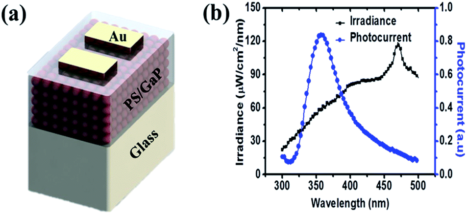 | ||
| Fig. 3 (a) Schematic illustration of device architecture (b) photocurrent response with the wavelength of monochromatic light. | ||
In conclusion, the facile synthesis of GaP NCs has been developed via hot injection method using gallium chloride (GaCl3) and tris(trimethylsilyl)phosphine ((TMS)3P) as precursors and 1-octadecene (ODE) and palmitic acid (PA) as coordinating solvents. The optical properties of GaP NCs analyzed through PL, PLE, and PL decay data suggest that the emission is a consequence of the quantum confinement effect. The optically active transitions result from the quantized levels of indirect and direct energy gaps. Interesting optical properties are also demonstrated device: UV detector based on the GaP NCs shows that the NCs produce excitons upon absorption of UV irradiation, resulting in photocurrent in the diode.
Acknowledgements
This work was supported by the New & Renewable Energy Core Technology Program of the Korea Institute of Energy Technology Evaluation and Planning (KETEP, no. 20133030000140 and 20133030011330), D. C. Lee and K. Lee acknowledge financial support from LG chem., Ltd. Basic Science Research Program through the National Research Foundation of Korea(NRF) funded by the Ministry of Science, ICT & Future Planning (no. 2014R1A5A1009799) and the Priority Research Centers Program (2012-0006687) and the National Research Foundation (NRF) grant funded by the Korean government (no. 2011-0030256), S. Kim, S. Jeong were supported by Global R&D Program funded by KIAT (no. 1415134409).Notes and references
- S. Coe, W.-K. Woo, M. G. Bawendi and V. Bulovic, Nature, 2002, 420, 803 CrossRef PubMed
.
- C. B. Murray, D. J. Norris and M. G. Bawendi, J. Am. Chem. Soc., 1993, 115, 8706 CrossRef CAS
- V. L. Klimov, A. A. Mikhailovsky, S. Xu, A. Malko, J. A. Hollingsworth, C. A. Leatherdale, H.-J. Eilser and M. G. Bawendi, Science, 2000, 290, 314 CrossRef CAS
- A. P. Alivisatos, Science, 1996, 271, 933 CAS
- E. Ryu, S. Kim, E. Jang, S. Jun, H. Jang, B. Kim and S.-W. Kim, Chem. Mater., 2009, 21, 573 CrossRef CAS
- X. Peng and D. Battaglia, Nano Lett., 2002, 2, 1027 CrossRef
- J. P. Zimmer, S.-W. Kim, S. Onishi, E. Tanaka, J. V. Frangioni and M. G. Bawendi, J. Am. Chem. Soc., 2006, 128, 2526 CrossRef CAS PubMed
- U. Banin, Y. W. Cao, D. Katz and O. Millo, Nature, 1999, 400, 542 CrossRef CAS PubMed
- D. Gammon, E. S. Snow, B. V. Shanabrook, D. S. Katzer and D. Park, Science, 1996, 273, 87 CAS
- J. Park and S.-W. Kim, J. Mater. Chem., 2011, 12, 3745 RSC
- L. Li, T. J. Daou, I. Texier, T. T. K. Chi, N. Q. Liem and P. Reiss, Chem. Mater., 2009, 21, 2422 CrossRef CAS
- C. Steinhagen, M. G. Panthani, V. Akhavan, B. Goodfellow, B. Koo and B. A. Kogel, J. Am. Chem. Soc., 2009, 131, 12554 CrossRef CAS PubMed
- P. Beecher, A. J. Quinn, E. V. Shevchenko, H. Weller and G. Redmond, Nano Lett., 2004, 4, 1289 CrossRef CAS
- W. Ma, J. M. Luther, H. Zheng, Y. Wu and A. P. Alivisatos, Nano Lett., 2009, 9, 1699 CrossRef CAS PubMed
- S. S. Kher and R. L. Wells, Chem. Mater., 1994, 6, 2056 CrossRef CAS
- O. I. Mićić, J. R. Sprague, C. J. Curtis, K. M. Jones, J. L. Machol and A. J. Nozik, J. Phys. Chem., 1995, 99, 7754 CrossRef
- Y. H. Kim, Y. W. Jun, B. H. Jun, S. M. Lee and J. W. Cheon, J. Am. Chem. Soc., 2002, 124, 13656 CrossRef CAS PubMed
- J. F. Janik, R. L. Wells, V. G. Young, A. L. Rheingold and I. A. Guzei, J. Am. Chem. Soc., 1998, 120, 532–537 CrossRef CAS
- F. S. Manciu, Y. Sahoo, D. J. MacRae, M. Furis, B. D. McCombe and P. N. Prasad, Appl. Phys. Lett., 2003, 82, 4059 CrossRef CAS PubMed
- S. Gao, J. Lu, N. Chen, Y. Zhao and Y. Xie, Chem. Commun., 2002, 3064 RSC
- J. Lauth, T. Strupeit, A. Kornowski and H. Weller, Chem. Mater., 2013, 25, 1377 CrossRef CAS
- B. J. Beberwyck and A. P. Alivisatos, J. Am. Chem. Soc., 2012, 134, 19977 CrossRef CAS PubMed
- Q. X. Zhang, Z. C. Zhang and B. P. Wang, J. Phys. D: Appl. Phys., 2008, 41, 185403 CrossRef
- A. L. Efros, M. Rosen, M. Kuno, M. Nirmal, D. J. Norris and M. Bawendi, Phys. Rev. B: Condens. Matter Mater. Phys., 1996, 54, 4843 CrossRef CAS
- S. E. Stokowski and D. D. Sell, Phys. Rev. B: Solid State, 1972, 5, 1636 CrossRef
- C. Delerue, G. Allan and M. Lannoo, Phys. Rev. B: Condens. Matter Mater. Phys., 1993, 48, 11024 CrossRef CAS
- L. Pavesi, L. Dal Negro, C. Mazzoleni, G. Franzo and F. Priolo, Nature, 2000, 408, 440 CrossRef CAS PubMed
- D. C. Lee, J. M. Pietryga, I. Robel, D. J. Werder, R. D. Schaller and V. I. Klimov, J. Am. Chem. Soc., 2009, 131, 3436 CrossRef CAS PubMed
- C. Delerue, G. Allan, C. Reynaud and O. Guillois, Phys. Rev. B: Condens. Matter Mater. Phys., 2006, 73, 235318 CrossRef
- L. E. Brus, P. F. Szajowski, W. L. Wilson, T. D. Harris, S. Schuppler and P. H. Cirtin, J. Am. Chem. Soc., 1995, 117, 2915 CrossRef CAS
- I. Vurgaftman, J. R. Meyer and L. R. Ram-Mohan, J. Appl. Phys., 2001, 89, 5815 CrossRef CAS PubMed
- M. V. Rama Krishna and R. A. Friesner, J. Chem. Phys., 1991, 95, 8309 CrossRef PubMed
- D. J. Chadi, Phys. Rev. B: Solid State, 1977, 16, 790 CrossRef CAS
- G. Dresseshaus, Phys. Rev., 1955, 100, 580 CrossRef
- Y. Long, Z. Zhao and C. Xu, Trans. Nonferrous Met. Soc. China, 2006, 16, 863 CrossRef
- J. R. Chelikowsky and M. L. Cohen, Phys. Rev. B: Solid State, 1976, 14, 556 CrossRef CAS
- Z. Zhaochun and L. Jianlin, Rare Met., 2011, 30, 510 CrossRef
- T. Wang and P. V. Radovanovic, J. Phys. Chem. C, 2011, 115, 18473 CAS
- D. R. Bakr and P. V. Kamat, Langmuir, 2010, 26, 11272 CrossRef PubMed
- O. I. Mićić, J. Sprague, Z. Lu and A. J. Nozik, Appl. Phys. Lett., 1996, 68, 3150 CrossRef PubMed
Footnotes |
| † Electronic supplementary information (ESI) available: Detailed experimental section, ICP-AES, HR-TEM, HR-XPS of GaP NCs, theoretical calculation of band gap energy, photoluminescence excitation (PLE) spectrum of GaP NCs at 405, 410, 415, and 420 nm. Additional single- and multi-exponential fits of PL decay of GaP NCs at (a) 400, (b) 450, (c) 500, and (d) 550 nm. See DOI: 10.1039/c4ra10115d |
| ‡ S. Kim and K. Lee contributed equally to this work. |
| This journal is © The Royal Society of Chemistry 2015 |