 Open Access Article
Creative Commons Attribution 3.0 Unported Licence
Antireflective gradient-refractive-index material-distributed microstructures with high haze and superhydrophilicity for silicon-based optoelectronic applications
Minkyu Choi,
Jung Woo Leem and
Jae Su Yu*
Department of Electronics and Radio Engineering, Kyung Hee University, 1732 Deogyeong-daero, Giheung-gu, Yongin-si, Gyeonggi-do 446-701, Republic of Korea. E-mail: jsyu@khu.ac.kr
First published on 11th March 2015
Abstract
We fabricate gradient-index (n) material-based microstructures, i.e., magnesium fluoride (MgF2, n ∼ 1.37) film-coated SU8 ultraviolet curable polymer (n ∼ 1.59) microcones (MCs) with tapered architectures, on silicon (Si, n ∼ 3.9) substrates using a soft imprint lithography method for high-performance Si-based optoelectronic applications. The effects of various geometry parameters (i.e., height, filling ratio, and period) of conical MCs on the SU8 film/Si structure including different thicknesses of MgF2 films on the reflectance properties are investigated by a theoretical analysis using a rigorous coupled-wave analysis simulation. For the fabricated samples, their optical characteristics and surface wetting behaviors are also explored. The MgF2 film-coated SU8 MCs on Si substrates (i.e., MgF2/SU8 MCs/Si) exhibit a superhydrophilic surface with very low water contact angles of <10° and reduce the surface reflection of the bare Si over a wide wavelength of 350–1100 nm, showing the lower average reflectance (Ravg) and solar weighted reflectance (Rsw) values of ∼14% and ∼12.1%, respectively, (i.e., Ravg ∼ 15.1% and Rsw ∼ 13% for the SU8 MCs/Si and Ravg ∼ 38.5% and Rsw ∼ 38% for the bare Si). Furthermore, the MgF2/SU8 MCs on glasses also show strong light scattering in transmissions at wavelengths of 350–1100 nm, which indicates an average haze ratio of ∼89.8%, while maintaining high total transmissions. Both the measured and calculated reflectance spectra showed similar results.
Introduction
Silicon (Si) is a key semiconductor material in optoelectronic device applications, such as photodetectors, solar cells, and light-emitting diodes, because of its fine properties including high purity, good electrical/optical characteristics, and thermal stability.1–4 However, the surface reflection of the Si is higher than 30% due to its high refractive index (high-n), which degrades the performance of Si-based optoelectronic devices. Thus, it is important to employ efficient antireflection coatings (ARCs) which can suppress unwanted Fresnel surface reflection losses. Over the past few years, due to some drawbacks of conventional quarter-wavelength multilayer-based ARCs with different dielectric materials including material selections, thermal expansion mismatch, and narrow bands of wavelengths and incident angles,5–7 bioinspired insect-eye micro- or nanoarchitectures which can considerably reduce the reflection in the wide ranges of incident wavelengths and angles have been widely studied.8–19 However, for a realization of microstructures or nanostructures, high-cost, low-throughput, and complex nanolithography techniques, e.g., laser interference,14,15 electron (e)-beam,16 and nanoimprint17 lithography methods and thermal18 and electrochemical19 treatments, together with a dry etching are usually required. On the other hand, the AR microstructures can be easily fabricated using a cost-effective, simple, fast, and high-throughput soft imprint lithography method.20–24 For conformable and elastomeric stamps, in most of reports on the soft lithography, polydimethylsiloxane (PDMS) with low free surface energy, flexibility, transparency, and hardness has been often used to transfer micro/nano patterns precisely on secondary substrates.20–24 For microstructured or nanostructured replicas, ultraviolet (UV) and thermally curable polymers have been utilized.25–28 These polymers are suitable for ARCs on the surface of the Si due to relatively low refractive indices of ∼1.4–1.7. In addition, the coverage of materials with a lower n on the textured surface of higher n materials would modify the refractive index profile, which further decreases the surface reflection due to the more gradient-refractive-index (GRIN) profile in terms of both the structures and materials.29–31 Besides, the microscale-based structures with larger periods than wavelengths of incident light can extend the effective optical paths and promote the transmitted diffuse lights, while keeping high total transmission properties (i.e., high optical haze).13,31–33 This light scattering effect can improve the light absorption in the optical and optoelectronic devices.33–35 Meanwhile, the superhydrophilicity makes water droplets to spread out evenly like a thin film on the surface. When a water droplet flows on the hydrophilic surface, it can squeeze into the space between the dusts and the surface, and then take the dusts away, i.e., self-cleaning.18,19,36 Also, it has many functions such as anti-fog, quick dry, and elimination of light scattering caused by the water droplets. This hydrophilicity can be enhanced if the roughness is sufficiently large.37,38 Our group has previously reported the antireflective GRIN material-distributed microstructures with a strong light scattering effect, together with an optical analysis.31 The micrograting structures were fabricated on the surface of transparent sapphires by conventional photolithography patterning and subsequent dry etching processes. As mentioned earlier, however, the realization of directly-patterned structures on the Si surface using these patterning and etching processes leads to the increase of the complexity and cost in the fabrication process. To avoid this problem, here, we proposed a novel architectural approach consisting of GRIN material-distributed microcone arrays, which effectively reduces the surface reflectivity of Si and enhances the light scattering in the Si, fabricated by the soft imprint lithography using the micrograting structured sapphires as a master mold and PDMS stamps. Although the master molds with microstructures are also prepared by the lithography patterning and etching processes, once master molds and replica polymer stamps are made, they can be repeatedly employed for pattern transfers into secondary substrates. Furthermore, the large-scale fabrication techniques (i.e., roll-to-roll and roll-to-plate processes) of master molds and stamps have been developed in the soft imprint lithography,39,40 which would facilitate the mass-production for industry applications. In addition, it is difficult to optimize experimentally efficient antireflective GRIN material-distributed microstructures with a strong light scattering effect on the Si surface due to high cost and time-consumption. To verify their optical properties with optimizing the structure, it is also necessary to perform numerical modeling and optical calculations. Therefore, it is very meaningful to analyze the optical properties and wetting behaviors of the GRIN material-based microstructures on the Si surface. In this work, we reported the optical design, fabrication, and characterization (i.e., optical properties and surface wettability) of magnesium fluoride (MgF2)-coated SU8 polymer microstructures on the Si surface via the soft imprint lithography and subsequent e-beam evaporation. For optical analyses, numerical modeling and simulations were carried out using the rigorous coupled-wave analysis (RCWA) and finite-difference time-domain (FDTD) methods.Numerical modeling details and simulations
Effect of geometry parameters on reflectance properties
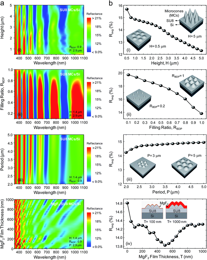
Firstly, the effects of various geometry parameters, such as height, filling ratio, and period, of conical MCs on the SU8 film/Si substrate on reflectance properties were investigated by the RCWA method using a commercial software (DiffractMOD, Rsoft Design Group). For the MgF2 film-coated SU8 MCs/Si structure (i.e., MgF2/SU8 MCs/Si), the reflection calculations were also performed as a function of MgF2 film thickness. Fig. 1 shows the (a) contour plots of variations of calculated reflectance spectra of the SU8 MCs/Si structure for different geometry parameters of (i) height, (ii) filling ratio, and (iii) period including the (iv) MgF2 film thickness of the MgF2/SU8 MCs/Si structure and (b) average reflectance (Ravg) values for the corresponding geometry parameters at wavelengths of 350–1100 nm. The fixed values for geometry parameters and three-dimensional (3D) scale-modified corresponding simulation models with 2D periodic hexagonal pattern arrays used in these calculations are also shown in the inset of Fig. 1(a) and (b), respectively. To design the numerical model, the geometry of the conical MCs was roughly represented in the Cartesian coordinate system by a scalar-valued function of three variables, f(x,y,z), for simplicity. The shape of conical MCs can be roughly defined by the following equations:27| r = RMCs × [(HMCs − z)/HMCs]1/OT and x2 + y2 = r2, (0 ≤ z ≤ HMCs), | (1) |
Angle-dependent reflectance properties
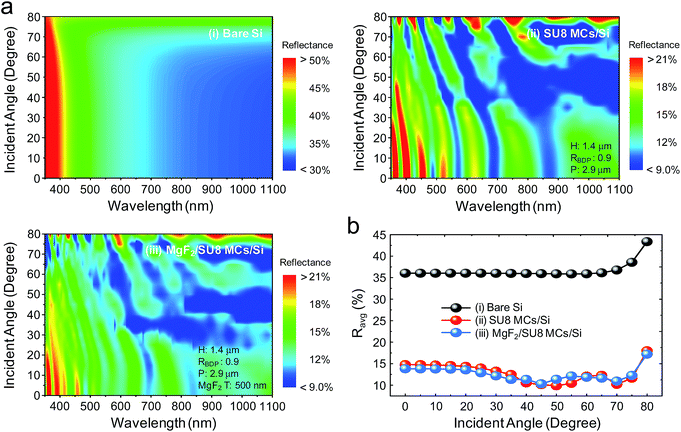
The conical micrograting structure can further suppress the surface reflection for the obliquely incident light due to its relatively omnidirectional shape.12 Fig. 2 shows the (a) contour plots of variations of calculated reflectance spectra of (i) the bare Si, (ii) the SU8 MCs/Si, and (iii) the MgF2/SU8 MCs/Si for different incident angles (θi) of 0–80° and (b) Ravg values of the corresponding structures as a function of incident angle for non-polarized light. In Fig. 2, the incorporation of conical SU8 MCs into the surface of Si results in considerably reduced reflection in the wide ranges of wavelengths and incident angles. The SU8 MCs/Si structure has a much lower Ravg value of ∼12.8% for θi values of 0–80° (i.e., Ravg ∼ 36.6% for the bare Si). Meanwhile, the MgF2/SU8 MCs/Si structure shows superior antireflective properties compared to the SU8 MCs/Si at θi values of <40° while it exhibits slightly higher Ravg values at some θi values of ≥40°. This may be attributed to the variation of effective optical path lengths, which is related to the interferences in diffracted and rebounded lights at the interfaces of air/MgF2 film, MgF2 film/SU8 MCs, and SU8 film/Si, caused by the change in the optical thickness of MgF2 film on the SU8 MCs/Si structure for larger oblique incident lights.49 Nevertheless, its Ravg value of ∼12.4% for the entire θi range of 0–80° is lower than those of both the bare Si (i.e., Ravg ∼ 36.6%) and the SU8 MCs/Si (i.e., Ravg ∼ 12.8%) samples. From these results, the conical microstructured polymer films can significantly suppress the surface reflection of Si over a wide range of wavelengths and incident angles. Moreover, the coating of materials with a lower n on the SU8 MCs/Si can further reduce the reflection.Results and discussion
Fabrication and characterization of SU8 MCs and MgF2 film coating
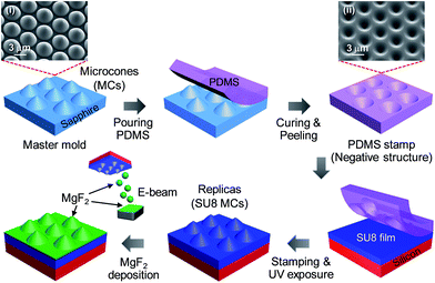
Fig. 3 shows the schematic diagram of process steps for the fabrication of MgF2 film-coated SU8 MCs on Si substrates via the soft lithography and e-beam evaporation. The scanning electron microscope (SEM) images of (i) sapphire master molds and (ii) PDMS stamps are also shown in Fig. 3. To form the MCs on SU8 polymer films, the patterned sapphire substrate, which was purchased from AND Corporation, consisting of conical MCs with 2D periodic hexagonal patterns was used as a master mold, having average height and period of ∼1.5 ± 0.1 and ∼2.9 ± 0.1 μm, as shown in the (i) SEM image of Fig. 3. In order to transfer MC patterns from the master mold into the Si substrate, Sylgard 184 (Dow Corning Co.) PDMS solution at a ratio of 10![[thin space (1/6-em)]](https://www.rsc.org/images/entities/char_2009.gif) :
:![[thin space (1/6-em)]](https://www.rsc.org/images/entities/char_2009.gif) 1 (base
1 (base![[thin space (1/6-em)]](https://www.rsc.org/images/entities/char_2009.gif) :
:![[thin space (1/6-em)]](https://www.rsc.org/images/entities/char_2009.gif) agent) was poured on master molds and then cured at a temperature of 75 °C for 2 h. After that, the PDMS stamps were carefully separated from the molds, thus creating the negative conical MC patterned PDMS stamps, as shown in the (ii) SEM image of Fig. 3. The SU8 (Micro Chem Corp.) negative photoresist which is one of UV curable polymers was spin-coated on Si substrates with a size of ∼20 mm × 20 mm. The substrates were ultrasonically cleaned in acetone, methanol, and de-ionized water for 10 min, respectively, and cured provisionally by pressing (3.0 kgf) the PDMS stamps. After UV exposure for 20 min, the MCs on the surface of SU8 film/Si substrates were formed by peeling off the PDMS stamps. The MgF2 film was deposited on SU8 MCs/Si samples by using an e-beam evaporation system at room temperature with a rotation speed of 10 rpm. The deposition rate was kept at 2 Å s−1 using a quartz crystal sensor for thickness monitoring and rate control. The MgF2 film-coated SU8 MCs were also prepared on the soda lime float glass substrates (Microscope slides, Sail brand, Cat. no. 7101, manufactured by Yancheng Huida medical instruments Co., China).
agent) was poured on master molds and then cured at a temperature of 75 °C for 2 h. After that, the PDMS stamps were carefully separated from the molds, thus creating the negative conical MC patterned PDMS stamps, as shown in the (ii) SEM image of Fig. 3. The SU8 (Micro Chem Corp.) negative photoresist which is one of UV curable polymers was spin-coated on Si substrates with a size of ∼20 mm × 20 mm. The substrates were ultrasonically cleaned in acetone, methanol, and de-ionized water for 10 min, respectively, and cured provisionally by pressing (3.0 kgf) the PDMS stamps. After UV exposure for 20 min, the MCs on the surface of SU8 film/Si substrates were formed by peeling off the PDMS stamps. The MgF2 film was deposited on SU8 MCs/Si samples by using an e-beam evaporation system at room temperature with a rotation speed of 10 rpm. The deposition rate was kept at 2 Å s−1 using a quartz crystal sensor for thickness monitoring and rate control. The MgF2 film-coated SU8 MCs were also prepared on the soda lime float glass substrates (Microscope slides, Sail brand, Cat. no. 7101, manufactured by Yancheng Huida medical instruments Co., China).
The surface and cross-sectional morphologies of the samples were characterized by using a SEM (LEO SUPRA 55, Carl Zeiss) system. The reflectance and transmittance properties were characterized by using a UV-vis-NIR spectrophotometer (Cary 5000, Varian) with an integrating sphere. The contact angles of water droplets were taken by using a contact angle measurement system (Phoenix-300, SEO Co., Ltd.) and averaged for three different positions on the surface of samples.
Structural properties and surface wetting behaviors
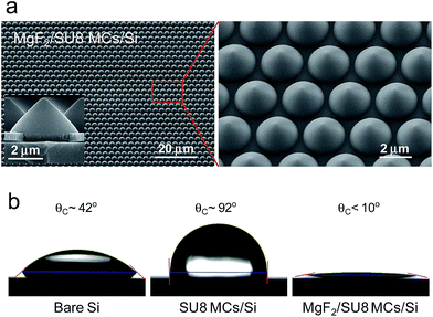
Fig. 4 shows (a) the 40°-tilted oblique- and side-view SEM images of the MgF2/SU8 MCs/Si sample and (b) the photographs of a water droplet on the surface of the bare Si, the SU8 MCs/Si, and the MgF2/SU8 MCs/Si samples. From the SEM images of Fig. 4(a), it can be observed that the conical MCs on SU8 film/Si substrates were well transferred from sapphire master molds via the PDMS stamps without any large deformation and distortion over a broad area. The MgF2 film with a thickness of 500 nm was also well deposited on the surface of SU8 MCs/Si samples. For the SU8 MCs, the average period and average height were also estimated to be ∼2.9 ± 0.1 and 1.4 ± 0.1 μm, respectively. The filling ratio of MCs was about RBDP ∼ 0.9.The surface wetting properties strongly depend on the structures and materials.37,50 As shown in Fig. 4(b), the bare Si exhibited a hydrophilic surface with a water contact angle (θC) of ∼42°. However, for the SU8 MCs, the θC value of ∼92° was obtained. This θC value is higher than that (i.e., θC ∼ 74°)26 of flat SU8 films without any patterns due to the increased roughness on the surface of SU8 films caused by the MCs, which can be explained by the Cassie–Baxter model.51 On the other hand, the MgF2 film-coated SU8 MCs/Si samples had very low θC values of <10°, indicating a superhydrophilic surface. This is due to the hydrophilic MgF2 film on the roughened MCs as proposed by the Wenzel's model.37 For the superhydrophilic surface, a water droplet can rapidly spread out and form a liquid film after falling onto the surface, and under the effect of gravity, the liquid film is easy to flow along the surface and takes dust particles or contaminants away.18,19,36 Therefore, these MgF2/SU8 MCs/Si structures with a superhydrophilic surface may self-clean the pollutants and quickly dry the rainwater on the surface of Si-based optoelectronic devices in real outdoor environments.36,52
Optical properties
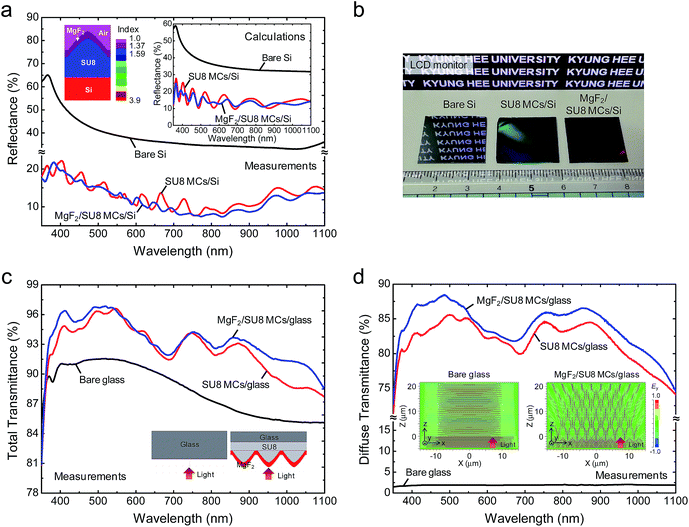
Measured reflectance spectra and 50°-titled oblique-view photographs of the bare Si, the SU8 MCs/Si, and the MgF2/SU8 MCs/Si samples are shown in Fig. 5(a) and (b), respectively. The refractive index profile (left) of MgF2/SU8 MCs/Si structure and calculated reflectance spectra (right) of the corresponding structures are also shown in the inset of Fig. 5(a). At wavelengths above 1030 nm, the abrupt increase in reflectance spectra is attributed to the backscattered lights from the back surface of the Si substrate because Si is transparent below its energy bandgap.53 As shown in Fig. 5(a), the SU8 MCs considerably reduce the reflection, exhibiting a much lower Ravg value of ∼15.1% than that of the bare Si (i.e., Ravg ∼ 38.5%). However, as confirmed in the calculated reflectance results in Fig. 1(d), the 500 nm-thick MgF2 film-coated SU8 MCs/Si can further decrease the reflectance compared to the SU8 MCs/Si over a wide wavelength of 350–1100 nm, showing the Ravg value of ∼14%. This is due to the formation of linear GRIN profile between air and the SU8 caused by the MCs and the step GRIN variation of the constituent materials from air (n = 1) to the Si (n ∼ 3.9) via the MgF2 (n ∼ 1.37)/SU8 (n ∼ 1.59), which can be seen in the left inset of Fig. 5(a), as well as the extension of effective optical path lengths caused by the diffracted and rebounded lights between the MCs.13,29,31–33,54,55 In fact, the MgF2/SU8 MCs/Si with the Ravg ∼ 14% exhibits a relatively poor antireflection performance compared to other nanostructures or thin films as ARCs for reducing the surface reflectivity of the Si. The nanostructures including subwavelength-structured nipple grating or hollow-tip arrays dramatically reduced the surface reflectivity of the bare Si (R values of >30%) by R values of <5% in the wavelength range of 400–1100 nm.47,56–59 The thin film-based ARCs such as single layer (e.g., SiN)60 or double layers (e.g., SiO2/TiO2)61 coated on the Si also showed Ravg values below than 10%. However, most of nanostructures for ARCs have been usually realized by expensive and complicated fabrication processes including colloidal-sphere,56,57 nanoimprint,58 and laser interference59 lithography techniques as well as thermally-dewetted metal nanoparticles47 with subsequent dry or chemical etching processes. On the other hand, the conventional ARCs consisting of a stack of thin-film dielectric layers can be fabricated by a relatively simple deposition or coating process. But, they also have some drawbacks such as poor or reduced substrate adhesion on certain materials due to the thermal expansion mismatch, sensitivity to thickness variations, and material selection as well as narrow low reflection band for incident wavelengths and angles,5–7 which may not be suitable in practical harsh environments. On the contrary, as mentioned earlier, in terms of the fabrication process for SU8 MCs, the soft imprint lithography is compatible with continuous processing, which is advantageous for simple, low-cost, and high-throughput production compared to other nanopatterning methods for etch mask patterns and subsequent dry etching processes.20–24 Master molds and stamps are also reusable. Additionally, mass production is possible by large-scale fabrication techniques for polymer stamps.39,40 Moreover, this pattern transfer technique can be also employed on various substrates including semiconductors, metals, and transparent materials. For photovoltaic device applications, it is necessary to investigate the solar weighted reflectance (Rsw), which is defined by the ratio of the usable photons reflected to the total useable photons, of samples. The Rsw can be estimated by normalizing the reflectance and the terrestrial air mass 1.5 global spectra integrated over a wavelength range of 350–1100 nm.3 For the MgF2/SU8 MCs/Si sample, the relatively lower Rsw value of ∼12.1% was obtained compared to the SU8 MCs/Si (i.e., Rsw ∼ 13%) as well as the bare Si (i.e., Rsw ∼ 38%). In the inset of Fig. 5(a), the reflectance spectra calculated by the RCWA method roughly show a similar trend with the measured data in Fig. 5(a). Also, their antireflective properties can be observed from the photograph in Fig. 5(b). The characters in the LCD monitor were strongly reflected by the surface of the bare Si. On the contrary, both the SU8 MCs/Si samples with and without the MgF2 film almost had a black surface due to their low reflectivity at visible wavelengths, as can be seen in Fig. 5(a). Also, rainbow (e.g., green or red)-like colors on their surfaces were shown due to the strong light diffraction property.To investigate the diffuse light scattering of SU8 MCs, the corresponding structures were also prepared on the surface of glasses. Measured total and diffuse transmittance spectra of the bare glass, the SU8 MCs/glass, and the MgF2/SU8 MCs/glass samples are shown in Fig. 5(c) and (d), respectively. As shown in Fig. 5(c), both the SU8 MCs/glass and MgF2/SU8 MCs/glass samples exhibited higher total transmission spectra than that of the bare soda lime glass, which shows the similar optical behavior reported in the previously-published literature,28,62 in the wide wavelength range of 350–1100 nm, indicating larger average transmittance (Tavg) and solar weighted transmittance (Tsw) values of ∼92.4% and ∼93% for the SU8 MCs/glass and ∼93.4% and ∼93.9% for the MgF2/SU8 MCs/glass, respectively, (i.e., Tavg ∼ 88.3% and Tsw ∼ 89.1% for the bare glass). Besides, for a periodic grating structure, when light enters into the grating with a period of Λ at normal incidence, the angle of the transmitted diffraction waves, θt,m, in the m-th diffraction order is given by the well-known grating equation:63
 | (2) |
Conclusions
The MgF2/SU8 MCs/Si consisting of GRIN-material structures were fabricated by the soft imprint lithography using sapphire master molds with 2D periodic hexagonal conical micrograting pattern arrays. In comparison with both the SU8 MCs/Si and bare Si, their antireflective properties were experimentally and theoretically investigated, including their surface wetting behaviours. The coating of MgF2 film on the SU8 MCs/Si structure led to the reduction of reflection as well as the enhancement of diffused lights in transmissions. The MgF2/SU8 MCs/Si sample had a superhydrophilic surface (i.e., θC values of <10°) and exhibited lower Ravg and Rsw values of ∼14% and ∼12.1%, respectively, at wavelengths of 350–1100 nm (i.e., Ravg ∼ 15.1% and Rsw ∼ 13% for the SU8 MCs/Si and Ravg ∼ 38.5% and Rsw ∼ 38% for the bare Si, respectively). Additionally, it showed strong light diffraction with a Havg value of ∼89.8% over a wide wavelength region of 350–1100 nm. These results can provide a better insight into the broadband wide-angle antireflection microstructures, which can be easily prepared by the simple and inexpensive soft lithography, with self-cleaning functioned superhydrophilic and large diffuse light scattering properties for the fabrication of high-performance Si-based optoelectronic devices.Acknowledgements
This work was supported by the National Research Foundation of Korea (NRF) grant funded by the Korea government (MSIP) (no. 2013-068407).Notes and references
- Z. Huang, J. E. Carey, M. Liu, X. Guo, E. Mazur and J. C. Campbell, Appl. Phys. Lett., 2006, 89, 033506 CrossRef.
- C. P. Liu, J. Xin, L. Wang, J. J. Song, A. Y. S. Lee and P. Ho, RSC Adv., 2014, 4, 34669 RSC.
- J. W. Leem, M. Choi and J. S. Yu, ACS Appl. Mater. Interfaces, 2015, 7, 2349 CAS.
- M. A. Green, J. Zhao, A. Wang, P. J. Reece and M. Gal, Nature, 2001, 412, 805 CrossRef CAS PubMed.
- S. M. Yang, Y. C. Hsieh and C. A. Jeng, J. Vac. Sci. Technol., A, 2009, 27, 336 CAS.
- P. Lalanne and G. M. Morris, Proc. SPIE, 1996, 2776, 300 CrossRef CAS.
- N. Kadakia, S. Naczas, H. Bakhru and M. Huang, Appl. Phys. Lett., 2010, 97, 191912 CrossRef.
- J. W. Leem, K. S. Chung and J. S. Yu, Curr. Appl. Phys., 2012, 12, 291 CrossRef.
- J. W. Leem, J. S. Yu, D. H. Jun, J. Heo and W. K. Park, Sol. Energy Mater. Sol. Cells, 2014, 127, 43 CrossRef CAS.
- W. L. Min, B. Jiang and P. Jiang, Adv. Mater., 2008, 20, 3914 CrossRef CAS.
- K. Kintaka, J. Nishii, A. Mizutani, H. Kikuta and H. Nakano, Opt. Lett., 2001, 26, 1642 CrossRef CAS PubMed.
- J. W. Leem, Y. M. Song and J. S. Yu, Nanoscale, 2013, 5, 10455 RSC.
- J. W. Leem, M. S. Kim and J. S. Yu, J. Opt. Soc. Am. B, 2013, 30, 1665 CrossRef CAS.
- J. W. Leem and J. S. Yu, Opt. Express, 2012, 20, A431 CrossRef CAS PubMed.
- Y. M. Song, S. J. Jang, J. S. Yu and Y. T. Lee, Small, 2010, 6, 984 CrossRef CAS PubMed.
- Y. Kanamori, M. Ishimori and K. Hane, IEEE Photonics Technol. Lett., 2002, 14, 1064 CrossRef.
- J. Tommila, V. Polojärvi, A. Aho, A. Tukiainen, J. Viheriälä, J. Salmi, A. Schramm, J. M. Kontio, A. Turtiainen, T. Niemi and M. Guina, Sol. Energy Mater. Sol. Cells, 2010, 94, 1845 CrossRef CAS.
- L. K. Verma, M. Sakhuja, J. Son, A. J. Danner, H. Yang, H. C. Zeng and C. S. Bhatia, Renewable Energy, 2011, 36, 2489 CrossRef CAS.
- J. Son, L. K. Verma, A. J. Danner, C. S. Bhatia and H. Yang, Opt. Express, 2011, 19, A35 CrossRef CAS PubMed.
- D. Qin, Y. Xia and G. M. Whitesides, Nat. Protoc., 2010, 5, 491 CrossRef CAS PubMed.
- C. Y. Liu, K. J. Chen, D. W. Lin, C. Y. Lee, C. C. Lin, S. H. Chien, M. H. Shih, G. C. Chi, C. Y. Chang and H. C. Kuo, Opt. Express, 2014, 22, 4516 CrossRef CAS PubMed.
- G. Shao, J. Wu, Z. Cai and W. Wang, Sens. Actuators, A, 2012, 178, 230 CrossRef CAS.
- J. K. Choi, J. K. Jin, M. L. Jin, C. J. An and H. T. Jung, RSC Adv., 2014, 4, 12302 RSC.
- J. K. Y. Ong, D. Moore, J. Kane and R. F. Saraf, ACS Appl. Mater. Interfaces, 2014, 6, 14278 CAS.
- J. Bian, X. Fu, J. Hu, Y. Cui, Z. Li, C. Yuan, H. Ge, W. D. Li and Y. Chen, RSC Adv., 2014, 4, 22155 RSC.
- S. H. Lee, J. W. Leem and J. S. Yu, Opt. Express, 2013, 21, 29298 CrossRef PubMed.
- J. W. Leem, S. Kim, S. H. Lee, J. A. Rogers, E. Kim and J. S. Yu, Adv. Energy Mater., 2014, 4, 1301315 Search PubMed.
- J. W. Leem, X. Y. Guan, M. Choi and J. S. Yu, Sol. Energy Mater. Sol. Cells, 2015, 134, 45 CrossRef CAS.
- J. W. Leem, Y. M. Song and J. S. Yu, Opt. Express, 2011, 19, A1155 CrossRef CAS PubMed.
- Y. H. Ko and J. S. Yu, Opt. Express, 2011, 19, 297 CrossRef CAS PubMed.
- Y. H. Ko and J. S. Yu, Opt. Express, 2011, 19, 15574 CrossRef CAS PubMed.
- Y. P. Chen, C. H. Lee and L. A. Wang, Nanotechnology, 2011, 22, 215303 CrossRef PubMed.
- B. Janthong, Y. Moriya, A. Hongsingthon, P. Sichanugrist and M. Konagi, Sol. Energy Mater. Sol. Cells, 2013, 119, 209 CrossRef CAS.
- S. J. Tark, M. G. Kang, S. Park, J. H. Jang, J. C. Lee, W. M. Kim, J. S. Lee and D. Kim, Curr. Appl. Phys., 2009, 9, 1318 CrossRef.
- Y. Nasuno, N. Kohama, K. Nishimura, T. Hayakawa, H. Taniguchi and M. Shimizu, Appl. Phys. Lett., 2006, 88, 071909 CrossRef.
- S. Nishmoto and B. Bhushan, RSC Adv., 2013, 3, 671 RSC.
- R. N. Wenzel, Ind. Eng. Chem., 1936, 28, 988 CrossRef CAS.
- J. W. Leem, J. S. Yu, J. Heo, W. K. Park, J. H. Park, W. J. Cho and D. E. Kim, Sol. Energy Mater. Sol. Cells, 2014, 120, 555 CrossRef CAS.
- F. C. Krebs, Sol. Energy Mater. Sol. Cells, 2009, 93, 465 CrossRef CAS.
- S. H. Ahn and L. J. Guo, ACS Nano, 2009, 3, 2304 CrossRef CAS PubMed.
- S. A. Boden and D. M. Bagnall, Appl. Phys. Lett., 2008, 93, 133108 CrossRef.
- J. W. Leem, Y. P. Kim and J. S. Yu, J. Opt. Soc. Am. B, 2012, 29, 357 CrossRef CAS.
- Y. Xiong, Z. Liu and X. Zhang, Appl. Phys. Lett., 2008, 93, 111116 CrossRef.
- S. Okazaki, J. Vac. Sci. Technol., B: Microelectron. Nanometer Struct.--Process., Meas., Phenom., 1991, 9, 2829 CrossRef CAS.
- C. M. Hsu, S. T. Connor, M. X. Tang and Y. Cui, Appl. Phys. Lett., 2008, 93, 133109 CrossRef.
- B. D. Park, J. W. Leem and J. S. Yu, Appl. Phys. B, 2011, 105, 335 CrossRef CAS.
- J. W. Leem and J. S. Yu, Thin Solid Films, 2011, 519, 3792 CrossRef CAS.
- J. W. Leem, J. S. Yu, Y. M. Song and Y. T. Lee, Phys. Status Solidi A, 2011, 208, 1902 CrossRef CAS.
- W. Zhou, M. Tao, L. Chen and H. Yang, J. Appl. Phys., 2007, 102, 103105 CrossRef.
- J. A. Howarter and J. P. Youngblood, Macromol. Rapid Commun., 2008, 29, 455 CrossRef CAS.
- A. B. D. Cassie and S. Baxter, Trans. Faraday Soc., 1944, 40, 546 RSC.
- J. Son, S. Kundu, L. K. Verma, M. Sakhuja, A. J. Danner, C. S. Bhatia and H. Yang, Sol. Energy Mater. Sol. Cells, 2012, 98, 46 CrossRef CAS.
- M. L. Kuo, D. J. Poxon, Y. S. Kim, F. W. Mont, J. K. Kim, E. F. Schubert and S. Y. Lin, Opt. Lett., 2008, 33, 2527 CrossRef PubMed.
- Y. M. Song, G. C. Park, S. J. Jang, J. H. Ha, J. S. Yu and Y. T. Lee, Opt. Express, 2011, 19, A157 CrossRef PubMed.
- Z. Zhao and M. A. Green, IEEE Trans. Electron Devices, 1991, 38, 1925 CrossRef.
- C. H. Sun, P. Jiang and B. Jiang, Appl. Phys. Lett., 2008, 92, 061112 CrossRef.
- Y. Li, J. Zhang, S. Zhu, H. Dong, Z. Wang, Z. Sun, J. Guo and B. Yang, J. Mater. Chem., 2009, 19, 1806 RSC.
- Z. Yu, H. Gao, W. Wu, H. Ge and S. Y. Chou, J. Vac. Sci. Technol., B: Microelectron. Nanometer Struct.--Process., Meas., Phenom., 2003, 21, 2874 CrossRef CAS.
- J. W. Leem, Y. M. Song, Y. T. Lee and J. S. Yu, Appl. Phys. B, 2010, 100, 891 CrossRef CAS.
- Y. J. Lee, D. S. Ruby, D. W. Peters, B. B. McKenzie and J. W. P. Hsu, Nano Lett., 2008, 8, 1501 CrossRef CAS PubMed.
- S. Y. Lien, D. S. Wuu, W. C. Yeh and J. C. Liu, Sol. Energy Mater. Sol. Cells, 2006, 90, 2710 CrossRef CAS.
- M. Rubin, Sol. Energy Mater., 1985, 12, 275 CrossRef CAS.
- E. Hecht, Optic, Addison Wesley, 4th edn, 2002, ch. 10 Search PubMed.
| This journal is © The Royal Society of Chemistry 2015 |

