Enhancement of photocatalytic activity of a two-dimensional GeH/graphene heterobilayer under visible light
Hao Jinab,
Ying Dai*a,
Xiang-Chao Maa,
Lin Yua,
Wei Weia and
Bai-Biao Huanga
aSchool of Physics, State Key Laboratory of Crystal Materials, Jinan, 250100, People’s Republic of China. E-mail: daiy60@sina.com
bDepartment of Materials Engineering, The University of British Columbia, Vancouver, V6T 1Z4, BC, Canada
First published on 2nd June 2015
Abstract
Searching for novel photocatalysts is one of the most important topics in photocatalytic fields. For this purpose, in the present work, the structural, electronic, and optical properties of GeH as well as a GeH/graphene heterointerface are studied based on hybrid density functional calculations including the nonlocal van der Waals correction. Our results show that the strain-engineered GeH monolayer captures a broad range of the solar spectrum. Moreover, photogenerated electron–hole pairs can be efficiently separated in the GeH/graphene heterojunction by formation of a Schottky barrier. Comparing to a pure GeH monolayer, the hybrid GeH/graphene complex displays an enhanced optical absorption in the visible region, suggesting powerful potential in energy and environmental applications.
1 Introduction
In the last several decades, great efforts have been made to extend the light absorption spectra of photocatalysts, e.g. TiO2, to the visible range by doping metal ions and/or non-metal ions.1–4 However, the photocatalytic activity of doped materials would be impaired by the thermal instability or the formation of carrier recombination centres due to the strong localized states within the band gap.4,5 To overcome the disadvantages of doping, composite photocatalysts were developed based on the energy exchange between materials with different electronic structures, which could efficiently separate the photogenerated electron–hole pairs as well as modulate the band gap due to the combined effect of their heterolayered structure.6–8 In addition, the emergence of two-dimensional (2D) materials (i.e. graphene and graphene-like materials) has opened up a new way of searching for efficient composite photocatalysts.9–11 For example, Wang et al. demonstrated that a ZnO photocatalyst hybridized with graphite-like C3N4 exhibits high performance of photocatalytic activity and enhanced stability against photocorrosion due to efficient charge separation.12 Du and coworkers reported that the optical response of the hybrid C3N4 and graphene composite is greatly enhanced in the visible light region.13Recently, Bianco et al. reported a novel graphene-like GeH, which has single-atom layers stacked in a 2D structure.14 And its electron mobility is reported to be five times higher than that of bulk germanium and ten times higher than that of silicon, which is expected to have potential applications in photocatalysis.15,16 Therefore, it is very interesting to study the photocatalytic ability of GeH, as well as the combined effect of hybrid GeH and graphene nanocomposites. Unfortunately, to the best of our knowledge, both experimental and theoretical investigations on this issue are still scarce.
Based on hybrid density functional calculations with the inclusion of the nonlocal van der Waals (vdW) correction, herein we study the structural, electronic and optical properties of GeH as well as a GeH/graphene bilayer. The results demonstrate that GeH has a tunable band gap by isotropic strain, which is suitable for visible and even infrared absorption. However it shows relatively low photocatalytic activity due to the high recombination rate of the charge carriers. Nevertheless, our investigation demonstrates that the introduced GeH/graphene heterointerface can not only promote the separation of photogenerated charge carriers with the formation of a Schottky barrier, but also enhances the optical response under the visible light region, enabling the development of more efficient visible light driven photocatalysts.
2 Computational methods
Our DFT calculations were carried out using the Vienna ab initio simulation package (VASP),17,18 with the projector augmented wave (PAW) method,19 and the Perdew–Burke–Ernzerhof (PBE) generalized gradient approximation (GGA) to the exchange-correlation functional.20 To account for the underestimation of the band gap in standard DFT calculations, the accurate electronic structures were calculated using the Heyd–Scuseria–Ernzerhof (HSE06) hybrid functional,21,22 in which the hybrid functional was mixed with 25% Hartree-Fock (HF) exact exchange. A damped vdW correction based on Grimme’s scheme was also incorporated to better describe the nonbonding interaction between GeH and the graphene monolayer.23A cutoff energy of 500 eV was used to truncate the plane-wave expansion of the wave functions. The first Brillouin zone was sampled with a Monkhorst-Pack grid of 5 × 5 × 1 for structure optimization and 9 × 9 × 1 for static calculation.24 The vacuum space was set to be 20 Å, which is large enough to avoid interactions between periodic images. The atomic positions were fully relaxed in all reported calculations using the conjugate gradient (CG) method to an energy convergence of 10−6 eV and force convergence of 10−2 eV Å−1.
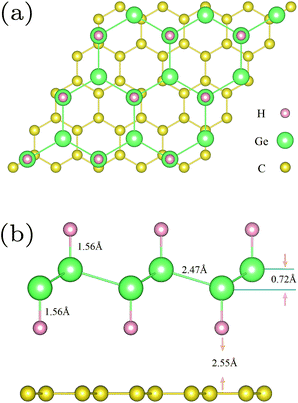
In order to simulate the hybrid GeH/graphene nanocomposite, a 5 × 5 graphene supercell with dimensions of 12.3 × 12.3 Å2 was used, which perfectly matched with a 3 × 3 GeH supercell. The optimized structure for the hybrid GeH/graphene complex is present in Fig. 1.
The binding energy between the monolayer GeH and graphene was obtained according to the following equation:
 | (1) |
To calculate the optical properties of the GeH/graphene nanocomposite, the frequency-dependent dielectric matrix was determined with the HSE06 functional. The imaginary part was calculated by a summation over empty states using the equation:25
 | (2) |
 | (3) |
3 Results and discussion
As shown in Fig. 1, the germanium atoms form a honeycomb structure with the buckling of the germanium plane of 0.72 Å. The hydrogen atoms bond to the Ge atoms on both sides of the plane in an alternating manner. The Ge–Ge and Ge–H bond lengths are 2.47 Å and 1.56 Å, respectively. The equilibrium distance between the graphene monolayer and GeH is calculated to be 2.55 Å. The heterointerface binding energy is obtained according to eqn (1) with the value of 0.84 J m−2. This value is about 3 times larger than that of the graphene/g-C3N4 complex,13 and one order of magnitude larger when compared with the GeH/TiO2(101) composite,15 indicating a very high stability.In order to understand the prospective photocatalytic performance of GeH/graphene heterojunctions, we first studied the electronic structures of the GeH monolayer using hybrid functional calculations. The band structures of GeH are shown in Fig. 2(a). It can be seen that the GeH monolayer has a direct band gap of 1.61 eV at Γ, in good agreement with recent experiments.14,16 In addition, the results of the band edge positions suggest that GeH has suitable redox potentials, with the oxidation potential (VO2/H2O) slightly below the valence band, while the reduction level (VH+/H2) is in between the gap.
Previous studies have demonstrated that tensile stress could drive the GeH monolayer into a topological insulator (TI).27,28 To better understand the influence of the strain on photocatalytic response, here we investigate the strain dependence of the band gap of the GeH monolayer. The tensile or compressive stress is uniformly applied and the crystal symmetries are maintained. The isotropic strain is defined as ε = Δa/a0, where the lattice constants of strained and unstrained supercells refer to a0 + Δa and a0, respectively. The calculated band gaps as a function of strain are plotted in Fig. 2(b).
The results show that when tensile stress is applied, Ge–Ge bonding is weakened due to the increased bond length, hence the splitting of bonding and antibonding states is decreased, leading to the reduction of the band gap. If the tensile stress is high enough, the valence band maximum (VBM) and conduction band minimum (CBM) of GeH degenerate at the Fermi level at Γ, and the system becomes a semimetal.27 In contrast, when the system undergoes compression, the splitting of bonding and antibonding states is increased linearly, giving rise to the larger band gap. Consequently, our results show that the strain-engineered GeH monolayer will capture a broad range of the solar spectrum.
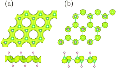
Despite these advanced properties, there are also some drawbacks for GeH. As shown in Fig. 2(c), the VBM is mainly composed of Ge 4p orbitals, whereas the CBM is composed of the Ge 4s and 4p mixed states. The charge density distributions of VBM and CBM largely overlap (see Fig. 3). As a result, the photoexcited electrons have high possibilities to fall back to the valence band, leading to low photocatalytic activity. The high recombination rate of the photogenerated electron–hole pairs hinders the practical applications of GeH. To overcome this problem, a GeH/graphene heterostructure is employed.
 | ||
| Fig. 3 The charge distribution of the (a) valence band and (b) conduction band at Γ with an isovalue of 0.01 e Å−3. | ||
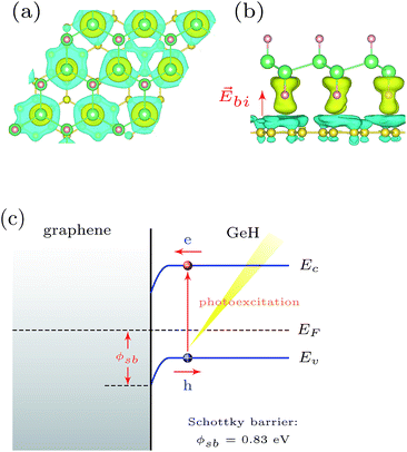
Upon formation of the interface, our calculations suggest a redistribution of the ground state charge in the system. In Fig. 4(a) and (b), the three-dimensional charge density difference is plotted, which is obtained by subtracting the charge density of the hybrid GeH/graphene complex from that of the independent GeH and graphene monolayers. It can be clearly seen that there is a space charge region within the GeH/graphene heterointerface. This can be understood based on the fact that hydrogen has a strong ability to attract the extra electrons. When graphene adheres to the GeH monolayer, the interaction between carbon and hydrogen atoms exerts a driving force, which leads to the electron transfer from the areas of graphene to the areas of GeH monolayer, while holes move in the opposite way. As shown in Fig. 4(b), when the charge redistribution in the GeH/graphene heterointerface reaches equilibrium, a built-in electric field (![[E with combining right harpoon above (vector)]](https://www.rsc.org/images/entities/i_char_0045_20d1.gif) bi) is induced. Since graphene is a semimetal and GeH is a semiconductor, the space charge region of the GeH/graphene heterointerface results in the formation of a Schottky barrier (ϕsb). The band bending associated with the Schottky barrier height is illustrated in Fig. 4(c).
bi) is induced. Since graphene is a semimetal and GeH is a semiconductor, the space charge region of the GeH/graphene heterointerface results in the formation of a Schottky barrier (ϕsb). The band bending associated with the Schottky barrier height is illustrated in Fig. 4(c).
To better understand the interface involved, we analyzed the band alignment and calculated the Schottky barriers by employing the lineup method.29,30 In the first step, we determined the work functions of the GeH and graphene monolayers, which are determined as the differences between the vacuum level and the Fermi energy. Based on the hybrid DFT results, the calculated work function of graphene is 4.54 eV, in good agreement with measured values in the range of 4.3–4.6 eV.9,10 The work function of the GeH monolayer is 5.64 eV, about 24% larger than that of graphene. The Schottky barrier at the GeH/graphene heterointerface was then determined as the difference between the Fermi energy of the bilayer and the VBM energy in an isolated GeH monolayer, corrected by the interface dipole potential as detailed in the work by Shan et al.29 The calculated ϕsb is 0.83 eV for holes to diffuse from graphene to GeH. Thus, when charge carriers are photoexcited, photogenerated holes in the valence band of GeH are trapped due to the Schottky barrier, whereas the photogenerated electrons can freely diffuse from the conduction band of GeH to graphene (see Fig. 4(c)). Therefore, photoexcited charge carriers can be separated effectively at the GeH/graphene heterojunctions, which leads to higher energy utilization efficiency and improves the photocatalytic performance.
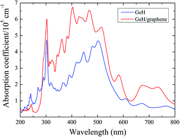
In order to investigate the visible light absorption ability of the GeH/graphene heterointerface, we calculated the optical absorption spectrum, which is obtained using eqn (3). As shown in Fig. 5, we found that HSE06-computed results can successfully reproduce the experimentally observed optical absorption spectrum of the GeH monolayer.16 Our calculations demonstrate that the GeH/graphene bilayer shows an enhanced absorption, with integrated intensity up to 2 times larger than the GeH monolayer. In addition, the absorption spectrum of the hybrid complex has been expanded into the orange-red region of the visible spectrum compared with the pure GeH monolayer, indicating that the hybrid GeH/graphene nanocomposite could harvest a broader range of visible light efficiently.
 | ||
| Fig. 5 The calculated optical absorption for the GeH monolayer and GeH/graphene complex as a function of wavelength. | ||
4 Conclusion
In this work, the structural and electronic properties of GeH as well as its band alignment with graphene were studied using hybrid functional DFT calculations with the inclusion of the nonlocal vdW correction. Our results demonstrate that the strain-engineered GeH monolayer will capture a broad range of the solar spectrum. Moreover, the interactions within the hybrid GeH/graphene complex lead to charge redistribution, which induces the built-in electric field and forms a Schottky barrier. Further analysis indicates that such heterointerfaces could be beneficial to facilitate the photogenerated charge separation, and enhance the optical response of the GeH monolayer under visible light. Thus, it is proposed that the GeH/graphene composite may be a powerful visible light driven photocatalyst.Acknowledgements
This work is supported by the National Basic Research Program of China (973 program, 2013CB632401), National Natural Science foundation of China under Grants 21333006 and 11374190, and the Fund for Doctoral Program of National Education 20120131110066.References
- R. Asahi, T. Morikawa, T. Ohwaki, K. Aoki and Y. Taga, Science, 2001, 293, 269–271 CrossRef CAS PubMed.
- S. Khan, M. Al-Shahry and W. Ingler, Science, 2002, 297, 2243–2245 CrossRef CAS PubMed.
- H. Jin, Y. Dai, W. Wei and B.-B. Huang, J. Phys. D: Appl. Phys., 2008, 41, 195411 CrossRef.
- Z. Wang, Y. Liu, B. Huang, Y. Dai, Z. Lou, G. Wang, X. Zhang and X. Qin, Phys. Chem. Chem. Phys., 2014, 16, 2758–2774 RSC.
- W. Choi, A. Termin and M. R. Hoffmann, J. Phys. Chem., 1994, 98, 13669–13679 CrossRef.
- W. Wang, B. Huang, X. Ma, Z. Wang, X. Qin, X. Zhang, Y. Dai and M.-H. Whangbo, Chem.–Eur. J., 2013, 19, 14777–14780 CrossRef CAS PubMed.
- H. Cheng, B. Huang, P. Wang, Z. Wang, Z. Lou, J. Wang, X. Qin, X. Zhang and Y. Dai, Chem. Commun., 2011, 47, 7054–7056 RSC.
- R. Zhang, Y. Dai, Z. Lou, Z. Li, Z. Wang, Y. Yang, X. Qin, X. Zhang and B. Huang, CrystEngComm, 2014, 16, 4931–4934 RSC.
- Q. Tang and Z. Zhou, Prog. Mater. Sci., 2013, 58, 1244–1315 CrossRef CAS PubMed.
- G. Xie, K. Zhang, B. Guo, Q. Liu, L. Fang and J. R. Gong, Adv. Mater., 2013, 25, 3820–3839 CrossRef CAS PubMed.
- Y. Ma, Y. Dai, M. Guo and B. Huang, Phys. Rev. B: Condens. Matter Mater. Phys., 2012, 85, 235448 CrossRef.
- Y. Wang, R. Shi, J. Lin and Y. Zhu, Energy Environ. Sci., 2011, 4, 2922–2929 CAS.
- A. Du, S. Sanvito, Z. Li, D. Wang, Y. Jiao, T. Liao, Q. Sun, Y. H. Ng, Z. Zhu, R. Amal and S. C. Smith, J. Am. Chem. Soc., 2012, 134, 4393–4397 CrossRef CAS PubMed.
- E. Bianco, S. Butler, S. Jiang, O. D. Restrepo, W. Windl and J. E. Goldberger, ACS Nano, 2013, 7, 4414–4421 CrossRef CAS PubMed.
- M. Niu, D. Cheng and D. Cao, Sci. Rep., 2014, 4, 4810 CAS.
- Z. Liu, Z. Lou, Z. Li, G. Wang, Z. Wang, Y. Liu, B. Huang, S. Xia, X. Qin, X. Zhang and Y. Dai, Chem. Commun., 2014, 50, 11046–11048 RSC.
- G. Kresse and J. Furthmüller, Phys. Rev. B: Condens. Matter Mater. Phys., 1996, 54, 11169–11186 CrossRef CAS.
- G. Kresse and J. Furthmüller, Comput. Mater. Sci., 1996, 6, 15–50 CrossRef CAS.
- G. Kresse and D. Joubert, Phys. Rev. B: Condens. Matter Mater. Phys., 1999, 59, 1758–1775 CrossRef CAS.
- J. P. Perdew, K. Burke and M. Ernzerhof, Phys. Rev. Lett., 1996, 77, 3865–3868 CrossRef CAS.
- J. Heyd, G. Scuseria and M. Ernzerhof, J. Chem. Phys., 2003, 118, 8207–8215 CrossRef CAS PubMed.
- J. Paier, M. Marsman, K. Hummer, G. Kresse, I. C. Gerber and J. G. Ángyán, J. Chem. Phys., 2006, 124, 154709 CrossRef CAS PubMed.
- S. Grimme, J. Comput. Chem., 2006, 27, 1787–1799 CrossRef CAS PubMed.
- H. J. Monkhorst and J. D. Pack, Phys. Rev. B: Condens. Matter Mater. Phys., 1976, 13, 5188–5192 CrossRef.
- M. Gajdoš, K. Hummer, G. Kresse, J. Furthmüller and F. Bechstedt, Phys. Rev. B: Condens. Matter Mater. Phys., 2006, 73, 045112 CrossRef.
- X. Li, J. Zhang and J. Yang, Sci. Rep., 2013, 3, 1858 Search PubMed.
- C. Si, J. Liu, Y. Xu, J. Wu, B.-L. Gu and W. Duan, Phys. Rev. B: Condens. Matter Mater. Phys., 2014, 89, 115429 CrossRef.
- Y. Ma, Y. Dai, C. Niu and B. Huang, J. Mater. Chem., 2012, 22, 12587–12591 RSC.
- B. Shan and K. Cho, Phys. Rev. B: Condens. Matter Mater. Phys., 2004, 70, 233405 CrossRef.
- M. Bernardi, M. Palummo and J. C. Grossman, Nano Lett., 2013, 13, 3664–3670 CrossRef CAS PubMed.
| This journal is © The Royal Society of Chemistry 2015 |


