Flexible piezoelectric nanogenerator based on Cu2O–ZnO p–n junction for energy harvesting
Jixue Leiab,
Bing Yinab,
Yu Qiuab,
Heqiu Zhangab,
Yue Changab,
Yingmin Luoa,
Yu Zhaoa,
Jiuyu Jic and
Lizhong Hu*ab
aSchool of Physics and Optoelectronic Technology, Dalian University of Technology, Dalian 116024, China. E-mail: lizhongh@dlut.edu.cn
bThe Key Laboratory for Micro/Nano Technology and System of Liaoning Province, Dalian University of Technology, Dalian 116024, People's Republic of China
cSchool of Information and Control Engineering, Liaoning Shihua University, Fushun 113001, People's Republic of China
First published on 24th June 2015
Abstract
In this study, a nanogenerator based on Cu2O–ZnO p–n junction has been fabricated on Cu wire substrates for harvesting mechanical energy from the environment. The flexible nanogenerator is composed of a Cu substrate, a Cu2O layer, ZnO nanorods and an outer Au-coated paper electrode; the Cu2O layer was obtained by oxidizing Cu wires directly and the ZnO nanorods were grown on the Cu2O layer using a low-temperature hydrothermal method. The existence of the Cu2O–ZnO p–n junction makes a contribution towards reducing the number of excess electrons in the ZnO, which facilitates in improving the output signal and also overcomes short circuits. An Au-coated paper electrode can involve more nanorods in the power generation process. The DC output voltage was up to 42 mV and the maximum output current density was 400 nA, which are approximately a 13-fold higher voltage and a one order of magnitude larger current in comparison to devices without a Cu2O layer, respectively. This study may provide important insight into a facile fabrication method for low-cost and high-performance energy harvesting devices.
I. Introduction
With the development of nanoscience and technology, methods of powering nanodevices have been widely investigated. Since the initial study in 2006 by Z. L. Wang's group1 on a nanogenerator (NG) based on the piezoelectric effect of ZnO nanostructures, this has been an active research field. A series of ZnO-based NGs on different substrates such as sapphire, ITO and fibers were developed.2–4 There are numerous sources of low frequency mechanical energy in our environment such as ultrasonic waves, body movement, and irregular air flow. Various approaches have been developed for converting this mechanical energy into electric energy with a ZnO-based NG.2,5–10 However, because of the piezo-potential screening effect, the output current from a ZnO-based NG is limited.11–13In recent years, remarkable efforts have also been invested in enhancing the performance of ZnO-based NGs.14–22 According to previous reports,23 there are two main methods. One involves increasing the number of effective nanorods; the other involves reducing the number of excess electrons to reduce the screening effects on piezoelectric charge. As an alternative solution, a p-type oxide semiconductor was used for fabricating ZnO-based piezoelectric NGs to form a p–n heterojunction with n-type ZnO.24,25 Among these oxide semiconductors, Cu2O is a promising material due to its p-type conductivity and low cost.26,27 In this study, we present a simple, low cost approach for fabricating a flexible NG based on a Cu2O–ZnO p–n junction on Cu wire. When wrapped by an external Au-coated paper electrode, the NG can convert mechanical energy into electricity under an external force. The output voltage and current produced by the generator can reach up to 42 mV and 400 nA, respectively. It is indicated that this type of NG has a potential application in harvesting energy from the environment to power nanodevices.
II. Experimental section
Synthesis of Cu2O–ZnO p–n junction
First, copper wires with a diameter of 0.2 mm (99.9%) were cleaned in a dilute hydrochloric acid solution (1 mol L−1) for 1–3 min and used as substrates; then, the wires were rinsed with deionized water and dried in air for several minutes. The oxidation was carried out in air at a temperature of 550 °C for 3 min in a tubular furnace. After oxidation, the Cu–Cu2O wires were coated with a thin ZnO seed layer (∼20 nm) using room temperature radio frequency (RF) magnetron sputtering. The background pressure of the vacuum chamber was 1 × 10⁻⁴ Pa and argon at a pressure of 3.5 Pa was used as the sputtering gas. Then, ZnO nanorods (NRs) were synthesized using a hydrothermal approach with a solution composed of 30 mmol L−1 zinc acetate dihydrate and hexamethylenetetramine (molar ratio 1![[thin space (1/6-em)]](https://www.rsc.org/images/entities/char_2009.gif) :
:![[thin space (1/6-em)]](https://www.rsc.org/images/entities/char_2009.gif) 1). After incubating at 90 °C for 2 h, the substrates with ZnO NRs grown on them were removed from the solution, rinsed with deionized water and dried.
1). After incubating at 90 °C for 2 h, the substrates with ZnO NRs grown on them were removed from the solution, rinsed with deionized water and dried.
Fabrication of nanogenerator
The Cu2O–ZnO p–n junction NG (CZNG) is composed of a central as-grown Cu2O–ZnO p–n junction on a Cu substrate and an outer Au-coated paper electrode. For the fabrication of the flexible CZNG, one end of the sample was etched off locally using an HCl solution to expose the Cu, which acted as an electrode for making contact. A paper was coated with an Au layer by sputter deposition using an Emitech K575XD Turbo Sputter Coater, which acted as another electrode. The ZnO NR-coated Cu–Cu2O wires were all wrapped up with the flexible Au-coated paper.Characterization
The morphologies of the Cu2O layer and the as-grown ZnO–Cu2O samples were characterized by scanning electron microscopy (SEM; FEI NovaNanoSEM). X-ray diffraction (XRD) was used to analyze their crystal structure. Room temperature photoluminescence (PL) was performed using a He–Cd laser operating at a wavelength of 325 nm. A Keithley 4200 semiconductor characterization system was used to measure the output signals generated from the flexible CZNG.III. Results and discussion
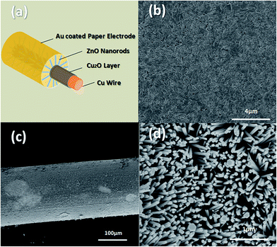
The structure of CZNG is shown in Fig. 1(a). It is composed of a Cu wire substrate, a Cu2O layer, ZnO NRs, and an Au-coated paper outer electrode. Fig. 1(b) shows the SEM images of the Cu2O layer. As shown, the Cu2O film is dense. Typical SEM images, under different magnifications, of ZnO nanorods grown on the Cu2O layer are shown in Fig. 1(c) and (d). The ZnO NRs grew radially and densely along the wires. All the ZnO NRs had a hexagonal cross-section with a diameter of ∼100 nm, indicating that their growth direction is parallel to the c-axis. The top and side surfaces of the ZnO NRs are smooth and clean, which makes it easy for them to form reliable metal–semiconductor junctions with the metal electrode.As shown in Fig. 2(a), X-ray diffraction (XRD) was used to characterize the crystalline phases of the Cu2O layer and ZnO NRs. From the XRD pattern of the as-prepared Cu2O layer, the peak positions could be easily assigned to the (111), (200), and (220) crystal planes of the cubic Cu2O structure. It should be noted that a finite CuO phase also exists; however, both CuO and Cu2O are p-type metal oxides, which can contribute to the formation of a p–n junction with ZnO. From the XRD pattern of ZnO/Cu2O/Cu, we can see that the ZnO NRs have a typical wurtzite structure, growing along the [002] direction. Fig. 2(b) illustrates the room-temperature PL spectrum of the sample. It exhibits a strong near band edge (NBE) emission at 380 nm. Moreover, the broad, deep-level, yellow emission (550–600 nm), which is related to the presence of structural defects or impurities, is negligible. This indicates that our sample has excellent crystal quality and low defect concentration. Besides, because the ZnO layer is considerably thick (∼5 μm), a few of the weaker peaks of CuO and Cu2O are not observed in the XRD pattern for ZnO/Cu2O/Cu.28
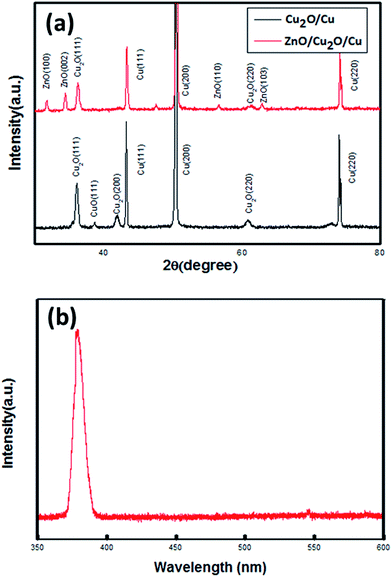 | ||
| Fig. 2 (a) XRD patterns of the Cu2O layer and ZnO NRs. (b) Room temperature photoluminescence spectrum of a CZNG sample. | ||
To measure the output current signals, a measuring setup was designed in this study. As shown in Fig. 3(a), a plastic board (PB) was fixed to a Teflon base at one end and the other end was freestanding. The PB was elastic and could be easily bent into different curvatures and circular arcs. The CZNG was then mounted on the fixed end of the PB with two electrode leads connected to a Keithley 4200 semiconductor characterization system. A manually applied stress was periodically introduced to deform the PB so that the CZNG experienced a cycling stretching–releasing deformation process. As shown in Fig. 3(b), when the CZNG becomes stressed, the ZnO NRs can rub against the Au-coated paper electrode and are thus deformed. A positive potential (V+) is produced at the stretched side of the NRs and a negative potential (V−) is induced at the compressed side; when the compressed side of the ZnO NRs is in contact with the electrode, a positively biased Schottky barrier is formed, and thus the electrons can flow freely across the interface to produce an output current.29 However, when the stretched side of the ZnO NRs is in contact with the electrode, the Schottky junction between Au and ZnO is reverse-biased, the electrons cannot overcome the barrier to reach the other side, thus very little current flows across the interface.
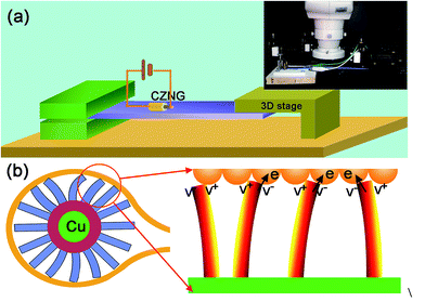 | ||
| Fig. 3 (a) Schematic diagram of the measuring setup. (b) The current generation process of the CZNG under strain. | ||
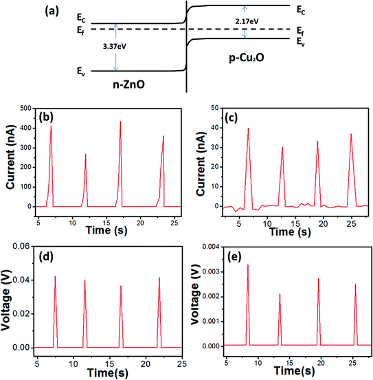
For current measurement, the short circuit is the key problem to be solved. Several attempts have been made to address this problem by coating a layer of polymethyl-methacrylate (PMMA) on the NRs,15,30 but this involves a complex production process and may decrease the stability of the devices. In our study, the Cu2O layer was used to overcome the short circuit. In addition to preventing the short circuit, the Cu2O layer also makes a contribution to the enhancement of the output signals. This is mainly because the number of excess electrons screening the piezoelectric potential is reduced in the ZnO. A Cu2O–ZnO p–n junction is made as a result of the addition of the Cu2O layer, forming a depletion region near the junction boundary, and thus the electron density in ZnO NRs is decreased. Fig. 4(a) shows the corresponding energy band diagram. During the power generation process, the residual free electrons in the conduction band of the ZnO NRs flow into piezoelectric potential areas to balance the piezoelectric potential. As the electron density is greatly decreased by the Cu2O–ZnO p–n junction, the screening effect is reduced and the piezoelectric output is enhanced.24,25 As shown in Fig. 4(b)–(e), the output current ability of CZNG is examined. The output voltage was up to 42 mV and the maximum output current was 400 nA, which represent approximately a 13-fold higher voltage and a one order of magnitude higher current in comparison to NGs without a Cu2O layer.
As previously mentioned, there is another approach for improving the performance of NGs, which is increasing the number of effective nanorods.31 For our structure, a foldable Au-coated paper acts as the external electrode, which can involve more nanorods in the power generation process. This is mainly embodied in two aspects. On the one hand, the flexible paper can wrap the Cu wire, and thus ensure that all the nanorods around the wire are in contact with the electrode. Compared with the spirally wound electrode used in previous reports,4,32 more nanorods take part in generating the piezoelectric power. On the other hand, the flexibility of paper offers a high contact probability between ZnO NRs with different lengths and the Au-coated paper-topped electrode under a bending mode. In the case of a top electrode with hard materials (Fig. 5(a)), the number of ZnO NRs making contact with the top electrode could be low because of the variation in the length or the tilted direction of the ZnO NRs. On the contrary, many more ZnO NRs could be in contact with the flexible paper electrode (Fig. 5(b)) because flexible paper can be deformed by an external force so as to touch NRs of different lengths. Thus, when Au-coated paper was used as the top electrode, we expected more active ZnO NRs to be in contact with the top electrode, increasing the generation efficiency.
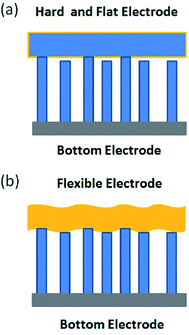 | ||
| Fig. 5 (a) Schematic of NGs with a hard and flat top electrode. (b) Schematic of NGs with a flexible top electrode. | ||
IV. Conclusion
In summary, we demonstrated a simple and low-cost approach to fabricate a nanogenerator based on a Cu2O–ZnO p–n junction. The Cu2O layer is formed by the direct oxidation of Cu wire, and then ZnO nanorods are synthesized using the hydrothermal method. Due to the Cu2O–ZnO p–n junction, the number of excess electrons in ZnO can be effectively reduced, which is beneficial to the piezoelectric signal output. In addition, a foldable Au-paper electrode is applied to fabricate the nanogenerator for more effective use of nanorods. A 13-fold higher output voltage and a one order of magnitude higher current were achieved in comparison with NGs without a Cu2O layer. This study may be significant with respect to designing and improving flexible piezoelectric nanogenerators.Acknowledgements
This work was supported by the Fundamental Research Funds for the Central Universities (DUT14LK35), the Foundation of Key laboratory for Micro/Nano Technology and System of Liaoning Province (20140405), the Foundation of Key laboratory for Micro/Nano Technology, the System of Liaoning and Province (20140405), and the Fundamental Research Funds for the Central Universities (DUT15LAB15).References
- Z. L. Wang and J. H. Song, Science, 2006, 312, 242–246 CrossRef CAS PubMed.
- X. D. Wang, J. H. Song, J. Liu and Z. L. Wang, Science, 2007, 316, 102–105 CrossRef CAS PubMed.
- C. J. Chang, Y. H. Lee, C. A. Dai, C. C. Hsiao, S. H. Chen, N. P. D. Nurmalasari, J. C. Chen, Y. Y. Cheng, W. P. Shih and P. Z. Chang, Microelectron. Eng., 2011, 88, 2236–2241 CrossRef CAS PubMed.
- Y. Qin, X. D. Wang and Z. L. Wang, Nature, 2008, 451, 809–U805 CrossRef CAS PubMed.
- R. Yang, Y. Qin, C. Li, G. Zhu and Z. L. Wang, Nano Lett., 2009, 9, 1201–1205 CrossRef CAS PubMed.
- S. N. Cha, J. S. Seo, S. M. Kim, H. J. Kim, Y. J. Park, S. W. Kim and J. M. Kim, Adv. Mater., 2010, 22, 4726–4730 CrossRef CAS PubMed.
- L. Lin, Y. F. Hu, C. Xu, Y. Zhang, R. Zhang, X. N. Wen and Z. L. Wang, Nano Energy, 2013, 2, 75–81 CrossRef CAS PubMed.
- Y. F. Hu, C. Xu, Y. Zhang, L. Lin, R. L. Snyder and Z. L. Wang, Adv Mater., 2011, 23, 4068–4071 CrossRef CAS PubMed.
- Z. Li, G. A. Zhu, R. S. Yang, A. C. Wang and Z. L. Wang, Adv. Mater., 2010, 22, 2534–2537 CrossRef CAS PubMed.
- B. Saravanakumar, R. Mohan, K. Thiyagarajan and S. J. Kim, RSC Adv., 2013, 3, 16646–16656 RSC.
- Y. Gao and Z. L. Wang, Nano Lett., 2009, 9, 1103–1110 CrossRef CAS PubMed.
- J. Liu, P. Fei, J. H. Song, X. D. Wang, C. S. Lao, R. Tummala and Z. L. Wang, Nano Lett., 2008, 8, 328–332 CrossRef CAS PubMed.
- J. I. Sohn, S. N. Cha, B. G. Song, S. Lee, S. M. Kim, J. Ku, H. J. Kim, Y. J. Park, B. L. Choi, Z. L. Wang, J. M. Kim and K. Kim, Energ Environ. Sci., 2013, 6, 97–104 RSC.
- G. A. Zhu, R. S. Yang, S. H. Wang and Z. L. Wang, Nano Lett., 2010, 10, 3151–3155 CrossRef CAS PubMed.
- S. Xu, Y. Qin, C. Xu, Y. G. Wei, R. S. Yang and Z. L. Wang, Nat. Nanotechnol., 2010, 5, 366–373 CrossRef CAS PubMed.
- M. Lee, J. Bae, J. Lee, C. S. Lee, S. Hong and Z. L. Wang, Energ Environ. Sci., 2011, 4, 3359–3363 RSC.
- K. Y. Lee, B. Kumar, J. S. Seo, K. H. Kim, J. I. Sohn, S. N. Cha, D. Choi, Z. L. Wang and S. W. Kim, Nano Lett., 2012, 12, 1959–1964 CrossRef CAS PubMed.
- Y. F. Hu, L. Lin, Y. Zhang and Z. L. Wang, Adv. Mater., 2012, 24, 110–114 CrossRef CAS PubMed.
- N. Jalali, P. Woolliams, M. Stewart, P. M. Weaver, M. G. Cain, S. Dunn and J. Briscoe, J. Mater. Chem. A, 2014, 2, 10945–10951 CAS.
- S. Lee, J. Lee, W. Ko, S. Cha, J. Sohn, J. Kim, J. Park, Y. Park and J. Hong, Nanoscale, 2013, 5, 9609–9614 RSC.
- X. L. Yue, Y. Xi, C. U. Hu, X. M. He, S. G. Dai, L. Cheng and G. Wang, RSC Adv., 2015, 5, 32566–32571 RSC.
- Y. Yang, H. Tian, H. Sun, R. J. Xu, Y. Shua and T. L. Ren, RSC Adv., 2014, 4, 2115–2118 RSC.
- J. Liu, P. Fei, J. Zhou, R. Tummala and Z. L. Wang, Appl. Phys. Lett., 2008, 92, 173105 CrossRef PubMed.
- S. H. Shin, M. H. Lee, J. Y. Jung, J. H. Seol and J. Nah, J. Mater. Chem. C, 2013, 1, 8103–8107 RSC.
- Y. X. Nie, P. Deng, Y. Y. Zhao, P. L. Wang, L. L. Xing, Y. Zhang and X. Y. Xue, Nanotechnology, 2014, 25, 265501 CrossRef PubMed.
- M. Izaki, T. Shinagawa, K. T. Mizuno, Y. Ida, M. Inaba and A. Tasaka, J. Phys. D: Appl. Phys., 2007, 40, 3326–3329 CrossRef CAS.
- M. Deo, S. Mujawar, O. Game, A. Yengantiwar, A. Banpurkar, S. Kulkarni, J. Jog and S. Ogale, Nanoscale, 2011, 3, 4706–4712 RSC.
- T. Guo, Y. D. Luo, Y. J. Zhang, Y. H. Lin and C. W. Nan, Cryst. Growth Des., 2014, 14, 2329–2334 CAS.
- M. Y. Choi, D. Choi, M. J. Jin, I. Kim, S. H. Kim, J. Y. Choi, S. Y. Lee, J. M. Kim and S. W. Kim, Adv. Mater., 2009, 21, 2185–2189 CrossRef CAS PubMed.
- S. Lee, S. H. Bae, L. Lin, Y. Yang, C. Park, S. W. Kim, S. N. Cha, H. Kim, Y. J. Park and Z. L. Wang, Adv. Funct. Mater., 2013, 23, 2445–2449 CrossRef CAS PubMed.
- M. Lanza, M. Reguant, G. Zou, P. Lv, H. Li, R. Chin, H. Liang, D. Yu, Y. Zhang, Z. Liu and H. Duan, Adv. Mater. Interfaces, 2014, 1, 1300101 Search PubMed.
- J. Bae, M. K. Song, Y. J. Park, J. M. Kim, M. L. Liu and Z. L. Wang, Angew. Chem., Int. Ed., 2011, 50, 1683–1687 CrossRef CAS PubMed.
| This journal is © The Royal Society of Chemistry 2015 |

