
Nickel(II)-ethylenediamine tetraacetic acid sensitized silicon nanowire array: an efficient cocatalyst-free photocatalyst for photocatalytic hydrogen generation under simulated sunlight irradiation†
Cheng Huanga,
Shi-Zhao Kang*a,
Xiangqing Lia,
Dong Wangb,
Lixia Qina,
Deli Lua and
Jin Mu*a
aSchool of Chemical and Environmental Engineering, Shanghai Institute of Technology, 100 Haiquan Road, Shanghai 201418, China. E-mail: mujin@sit.edu.cn; kangsz@sit.edu.cn; Fax: +86 21 60873061; Tel: +86 21 60873061
bKey Laboratory of Molecular Nanostructure and Nanotechnology, Institute of Chemistry, Chinese Academy of Sciences and Beijing National Laboratory for Molecular Sciences, Beijing 100190, China
First published on 28th July 2015
Abstract
In the present work, a green efficient photocatalyst was prepared using a silicon nanowire array and nickel(II)-ethylenediamine tetraacetic acid to reap three benefits simultaneously: (1) efficient H2 evolution under sunlight irradiation, (2) avoidance of the potential environment and health hazards that arise from the release of nanomaterials, (3) achievement of a Pt-free photocatalyst. The experimental results indicate that the as-prepared photocatalyst possesses high performance towards photocatalytic H2 evolution from water under simulated sunlight irradiation. A rate of H2 evolution of approximately 2.2 L m−2 h−1 can be achieved under optimal conditions. Here, nickel(II)-ethylenediamine tetraacetic acid plays an important role in the photocatalytic process as both a sensitizer and a sacrificial reagent. The photocatalytic activity of the nickel(II)-ethylenediamine tetraacetic acid sensitized silicon nanowire array is obviously higher than that of the silicon nanowire array. The rate of H2 evolution can be enhanced by a factor of 4 when nickel(II)-ethylenediamine tetraacetic acid is used instead of ethylenediamine tetraacetic acid disodium. Besides, the photocatalytic H2 evolution was studied as a function of the length of silicon nanowires, the concentration of nickel(II)-ethylenediamine tetraacetic acid and pH. And the photocatalytic mechanism was preliminarily discussed.
Introduction
Photocatalytic hydrogen evolution on a semiconductor/electrolysis interface represents a promising approach to low cost, renewable and carbon-free fuel. However, this is a great challenge. It is very difficult to prepare a photocatalyst with high efficiency and long-term durability using earth-abundant materials. Therefore, the development of photocatalysts for photocatalytic H2 evolution has been a hot topic. A series of efficient photocatalysts including TiO2,1 CuS,2 titania@graphene nanoflakes,3 g-C3N4,4 black TiO2 nanotubes,5 ZnO/SnO2−x nanoparticles,6 C-doped CdIn2O4,7 ZnS–ZnO hybrid nanowires,8 CaTa2O6,9 Sn3O4 (ref. 10) etc. have been reported. Nevertheless, the activity of the photocatalysts needs be further enhanced under sunlight irradiation from the practical point of view.Silicon is abundantly available, environmentally friendly and possesses an optimal bandgap (1.12 eV) which almost ideally matches the solar spectrum,11 implying that it would be a promising candidate for photocatalytic hydrogen evolution driven by sunlight. However, Si is not yet widely used in the field of photocatalytic hydrogen evolution. The major problems are the photo-corrosion of Si in water and the strong reflection of incident light from the water-silicon substrate interface due to the high reflective index of Si,11,12 which makes Si powder and Si substrate unsuitable for photocatalytic hydrogen evolution. Therefore, it is necessary to overcome the drawbacks above before Si-based photocatalysts are applied. Compared with Si powder and Si substrate, Si nanowire array exhibits many noteworthy properties, such as large specific surface area, excellent broadband anti-reflection, short carrier transfer distance in the radial direction and so on,11,13 implying that it is possible to prepare efficient and stable Si-based photocatalysts using Si nanowire array if a suitable sacrificial reagent is chosen. Besides, many additional benefits may be reaped when Si nanowires array is used as a photocatalyst, including avoidance of the potential environment and health hazards that arise from the release of nanomaterials, convenience for separation of catalyst from water and application in a continuous flow system. Recently, there are many reports on the application of Si-based photocatalysts in the photoelectrochemical water-splitting.14–17 Unfortunately, to our best knowledge, the papers on the application of Si nanowires array in the field of photocatalytic hydrogen evolution from water are relatively scarce so far. As a result, it is meaningful to explore the application of Si nanowires array in the field of photocatalytic hydrogen evolution.
It is well known that dye sensitization is one of powerful strategies for researchers to enhance the photocatalytic activity and the visible-light harvesting of photocatalyst. The common sensitizers include porphyrin,18,19 phthalocyanine,20 eosin,21 and bipyridyl complexes.22 However, these dyes are expensive. Moreover, their synthetic routes often involve the use of toxic and expensive initial reactants. Therefore, it is important to research and develop an efficient and low-cost sensitizer. Ethylenediamine tetraacetic acid disodium (EDTA-Na) is an excellent electron donor which is widely used in the photocatalytic hydrogen evolution.23–25 In addition, many complexes composed of ethylenediamine tetraacetic acid and transition metal ions can effectively absorb visible light. Thus, we can speculate that these complexes would serve simultaneously as a sensitizer and a sacrificial reagent in the photocatalytic process. If they are combined with Si nanowires array, it is possible to fabricate an efficient and stable Si-based photocatalytic system for photocatalytic hydrogen evolution. Nevertheless, in most of the studies reported, EDTA-Na was only used as a sacrificial reagent rather than a sensitizer. It is still unclear whether the complexes containing ethylenediamine tetraacetic acid and transition metal ions can server as a sensitizer or not.
In the present study, the nickel(II)-ethylenediamine tetraacetic acid (EDTA-Ni) sensitized silicon nanowires arrays were prepared. Meanwhile, the photocatalytic activity of the EDTA-Ni sensitized silicon nanowires array was explored systematically for the photocatalytic H2 production. Finally, the photocatalytic mechanism was preliminarily discussed.
Experimental
Materials
P-type Si (100) wafers were purchased from Zhejiang crystal silicon material Co., Ltd. Ethanol, hydrogen peroxide, hydrofluoric acid, silver nitrate, nickel nitrate and ethylenediamine tetraacetic acid disodium were purchased from Sinopharm Chemical Reagent Co., Ltd. Acetone, concentrated sulfuric acid and concentrated nitric acid were purchased from Shanghai Titan Scientific Co., Ltd. All reagents were of analytical grade and used as received. Deionized water was used as solvent.Preparation of Si nanowire arrays
Silicon nanowires array (SiNWs) was prepared according to the procedure reported (Scheme 1).26 In a typical process, a p-type Si (100) wafer (1–10 Ω cm, 3 cm × 3 cm) was consecutively cleaned with acetone, ethanol, and deionized water. Then, the cleaned Si wafer was immersed into a piranha solution consisting of H2O2 and H2SO4 (1![[thin space (1/6-em)]](https://www.rsc.org/images/entities/char_2009.gif) :3, v/v) for 15 min at room temperature, followed by immersed into 5% HF for 1 min. Next, the Si wafer was immediately transferred into an etchant (25 mL) containing AgNO3 (0.02 mol L−1) and HF (0.08 mol L−1). To control the nanowires length, the etching time was set to be 15, 30, 60 and 120 min, respectively. Afterwards, the wafer was rinsed with water for 5 min, cleaned with dilute nitric acid (10 vol%) for at least 60 min (depending on the length of nanowires). Finally, the wafer was rinsed with water again and dried in an oven at 60 °C.
:3, v/v) for 15 min at room temperature, followed by immersed into 5% HF for 1 min. Next, the Si wafer was immediately transferred into an etchant (25 mL) containing AgNO3 (0.02 mol L−1) and HF (0.08 mol L−1). To control the nanowires length, the etching time was set to be 15, 30, 60 and 120 min, respectively. Afterwards, the wafer was rinsed with water for 5 min, cleaned with dilute nitric acid (10 vol%) for at least 60 min (depending on the length of nanowires). Finally, the wafer was rinsed with water again and dried in an oven at 60 °C.
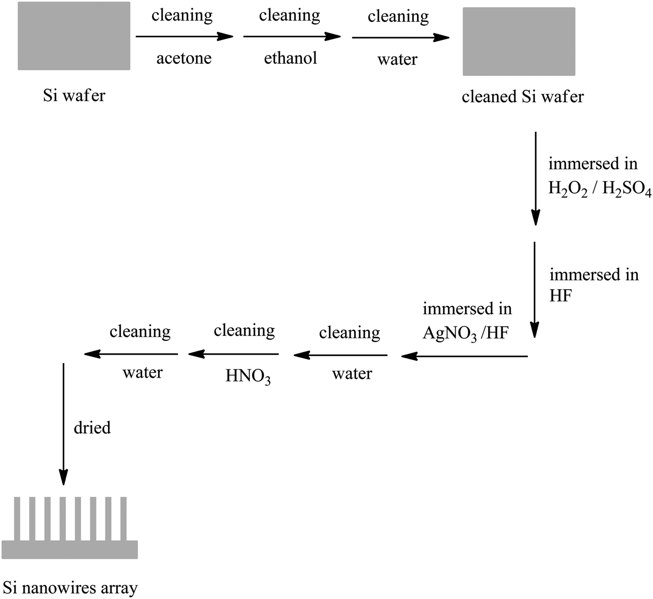 | ||
| Scheme 1 Schematic illustration of the Si nanowires array fabrication process. | ||
Photocatalytic activity test
The photocatalytic reaction was carried out in a gas-closed system with a reactor made of quartz. In a typical experiment, a 300 W xenon lamp equipped with an AM 1.5 G filter to simulate sunlight (263.7 mW cm−2) was employed as a light source. The distance between the lamp and the reactor is 1 cm. In a typical experiment, a Si wafer with SiNWs (3 cm × 3 cm) was put into the reactor containing EDTA-Ni aqueous solution (100 mL), and then the system was deaerated using N2. After the gas-closed system was vacuumed, turned on the power. The amounts of hydrogen produced were measured with a gas chromatograph (GC-7900, China, molecular sieve 5A, TCD) using N2 as a carrier gas, after a certain period of irradiation.Characterization
The scanning electron microscope (SEM) images were taken using a Hitachi S4800 scanning electron microscope (Japan). The UV-vis diffuse reflectance spectra were recorded on a Hitachi U-3900 UV-vis spectrophotometer (Japan). The UV-vis spectra of the solutions were measured with a Tianmei UV 1000 spectrophotometer (China). The N2 adsorption and desorption isotherm was measured on a Micromeritics ASAP-2020 nitrogen adsorption apparatus (USA). The electrochemical impedance spectroscopic (EIS) analyses of the samples were carried out using a CHI660E electrochemical system (Shanghai Chenhua Instruments, China) in a conventional three-electrode cell. The electrolyte solutions were EDTA-Ni/Na2SO4 mixed solution (0.025 mol L−1) and EDTA-Na/Na2SO4 mixed solution (0.025 mol L−1), respectively. The Si wafer with SiNWs (1 cm × 1.5 cm) was used as a work electrode. An Ag/AgCl electrode and a platinum electrode were used as the reference electrode and the counter electrode, respectively. Nitrogen was utilized for deaeration. The sinusoidal perturbation of 10 mV with a bias of −0.45 V was applied in the EIS analyses. The scanning frequency was in the range of 1–106 Hz. A 300 W Xe lamp equipped with an AM 1.5 G filter was used as a light source. The distance between the lamp and the reactor is 1 cm.Results and discussion
Fig. 1 shows the SEM images of SiNWs. It can be clearly observed from Fig. 1 that a well-aligned Si nanowires array is uniformly fabricated on the Si wafer. These nanowires are vertically oriented and aligned with high density. Their length and diameter are approximately 4 μm and 100 nm, respectively. Moreover, no other secondary nanostructures can be found on the nanowires. These results indicate that the Si nanowire array is fabricated on the Si substrate according to the procedure above. | ||
| Fig. 1 (A) Top view and (B) cross-section SEM images of the as-prepared SiNWs. | ||
Fig. 2A shows the UV-vis diffuse reflectance spectra of the as-prepared SiNWs and the bare Si substrate. As can be seen from Fig. 2A, the as-prepared SiNWs possesses excellent antireflective property. The reflectance of SiNWs is only 6.9% or more less in the range of 240–800 nm. In contrast, the planar Si substrate exhibits strong reflection with the highest reflectance of 93.8% at 284 nm. One possible explanation is that the Si nanowires array on the Si substrate may act as an optical buffer which can alleviate the mismatch in refraction indices between the planar Si wafer and air.27 Therefore, SiNWs demonstrates the significant light-trapping capability. Based on these experimental results, it can be concluded that SiNWs possesses excellent light absorption performance, which is favour to the photocatalytic hydrogen evolution.
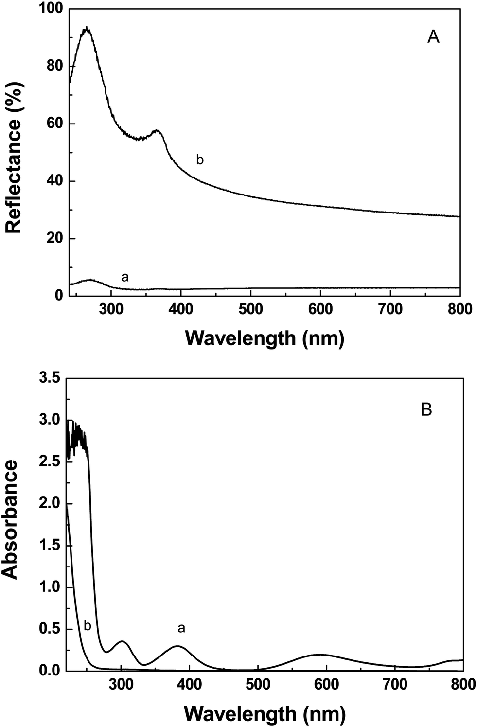 | ||
| Fig. 2 (A) UV-vis diffuse reflectance spectra of (a) the as-prepared SiNWs and (b) the Si substrate; (B) UV-vis spectra of (a) the EDTA-Ni aqueous solution (0.025 mol L−1) and (b) the EDTA-Na aqueous solution (0.025 mol L−1). | ||
Fig. 3 shows the time-courses of H2 evolution from EDTA-Ni aqueous solution over the as-prepared SiNWs (curve a) or the Si substrate (curve c) under simulated AM 1.5 G irradiation. For comparison, the time-courses of H2 evolution from EDTA-Na aqueous solution over the as-prepared SiNWs (curve b) or the Si substrate (curve d) are also shown in Fig. 3. As can be seen from Fig. 3a, the as-prepared SiNWs exhibits high photocatalytic activity for the H2 evolution in the EDTA-Ni aqueous solution. During the first 5 h irradiation, the mean rate of H2 evolution is up to 2.2 L m−2 h−1. The hydrogen production rate is almost constant in the first 9 h, and then it gradually decreases. The H2 production can be hardly observed after irradiated 19 h. The SEM image of SiNWs used (ESI Fig. S1†) shows that SiNWs possesses satisfactory stability. The morphology of SiNWs is steady during the photocatalytic process. Therefore, this gradually decreases may be ascribed to the back reaction of H2 on the surface of photocatalyst rather than the destruction of SiNWs. These results indicate that the SiNWs sensitized by EDTA-Ni is an efficient photocatalyst under simulated sunlight irradiation, and can keep the activity for a period of time.
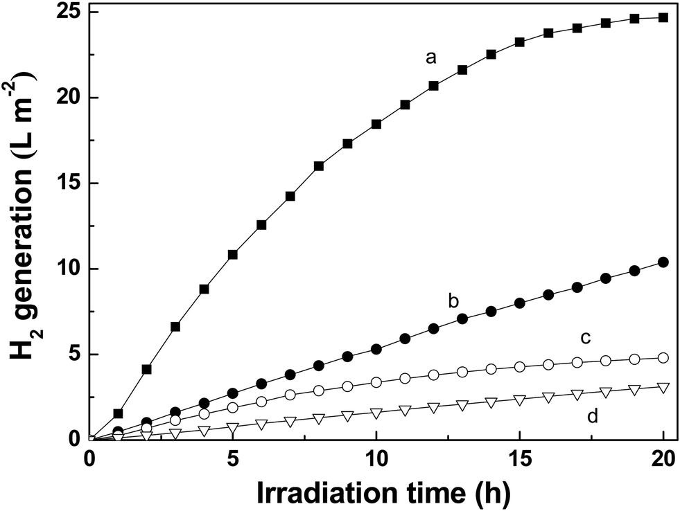 | ||
| Fig. 3 Time-courses of H2 evolution over (a) the as-prepared SiNWs in the EDTA-Ni aqueous solution, (b) the as-prepared SiNWs in the EDTA-Na aqueous solution, (c) the Si substrate in the EDTA-Ni aqueous solution and (d) the Si substrate in the EDTA-Na aqueous solution (photocatalyst: 3 cm × 3 cm SiNWs or 3 cm × 3 cm Si substrate; length of nanowires: 4 μm; EDTA-Ni aqueous solution: 0.025 mol L−1 100 mL, EDTA-Na aqueous solution: 0.025 mol L−1 100 mL; pH: 11). | ||
Furthermore, it can also be found that the photocatalytic activity of SiNWs is much higher than that of the flat Si substrate. When the EDTA-Ni solution is used, the hydrogen production rate over the as-prepared SiNWs exceeds that over the Si substrate by about five times. In addition, SiNWs shows obviously higher photocatalytic activity in the EDTA-Ni aqueous solution compared with that in the EDTA-Na solution. The photocatalytic activity of SiNWs is enhanced by about three times when the EDTA-Ni solution is used instead of the EDTA-Na solution. These phenomena indicate that the dramatic photocatalytic activity of SiNWs in the EDTA-Ni solution would be ascribed to the nanowires array structure and the reinforce effect of EDTA-Ni.
Based on the experimental results above, a possible mechanism is suggested as follows (Scheme 2). At first, when SiNWs is under irradiation, the electrons are excited from the valence band to the conduction band. Meanwhile, the electrons of EDTA-Ni are also excited and injected into the conduction band of Si. Then, protons are reduced into H2 by these photogenerated electrons. Here, the effects of the nanowires array structure can be assorted into three parts. (1) SiNWs possesses larger specific surface area in comparison with the planar Si substrate, which is favour to the photocatalytic hydrogen evolution. However, the Brunauer–Emmett–Teller (BET) measurement demonstrates that the apparent specific surface area of SiNWs is only 1.6 m2 g−1, implying that the surface area of the samples may not play an important role in this photocatalytic process. (2) The nanowires array structure would lead to enhancement of light harvesting because of the prolonged light absorbing length in the axial direction,13 which is confirmed by the UV-vis diffuse reflectance spectra (Fig. 2A). (3) The high aspect ratio and orientated structure of SiNWs is advantageous for the photo-generated carriers transfer.28 Similarly, the reinforce effect of EDTA-Ni can also be assorted into two parts. (1) The visible light absorption of the photocatalytic system can be effectively enhanced due to sensitization of EDTA-Ni. In order to confirm our assumption, the enhancement of the photocatalytic activity originated from the introduction of EDTA-Ni was explored using various light sources. And a rough photocatalytic activity enhancement factor (PF) was chosen as the scale to evaluate the enhancement of photocatalytic activity from EDTA-Ni. PF was calculated using the eqn (1):
| PF = (VEDTA-Ni − VEDTA-Na)/VEDTA-Na | (1) |
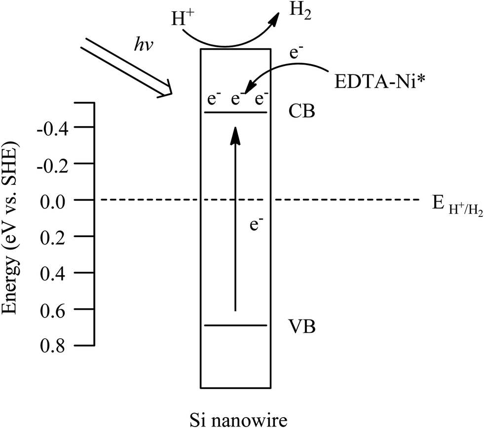 | ||
| Scheme 2 Schematic diagram for the photocatalytic H2 evolution over the EDTA-Ni sensitized SiNWs. | ||
| Light sources | Rate of H2 evolution (L m−2 h−1) | PF |
|---|---|---|
| AM 1.5 G (263.7 mW cm−2) | 2.41 (in EDTA-Ni solution) | 2.99 |
| 0.604 (in EDTA-Na solution) | ||
| Visible light (420 nm < λ < 800 nm, 179.8 mW cm−2) | 1.16 (in EDTA-Ni solution) | 2.92 |
| 0.295 (in EDTA-Na solution) | ||
| Visible light (590 nm < λ < 610 nm, 44.5 mW cm−2) | 0.968 (in EDTA-Ni solution) | 5.22 |
| 0.156 (in EDTA-Na solution) | ||
| UV light (77.3 mW cm−2) | 1.22 (in EDTA-Ni solution) | 1.70 |
| 0.449 (in EDTA-Na solution) |
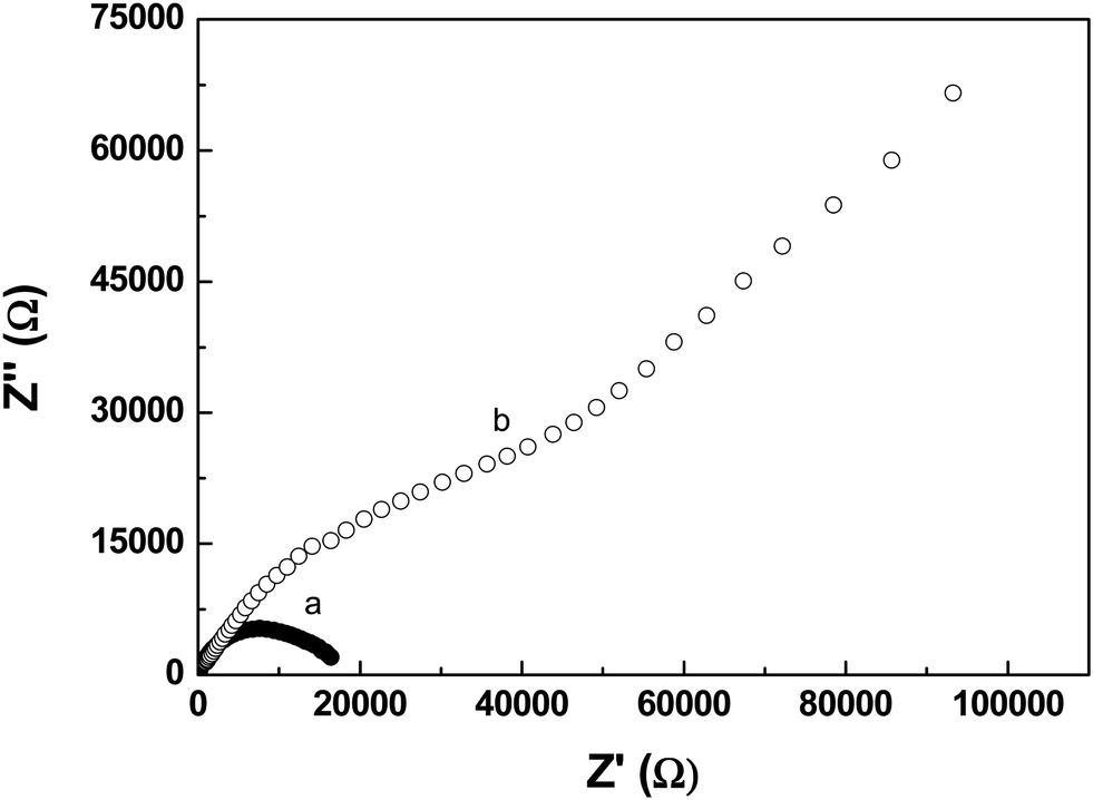 | ||
| Fig. 4 Nyquist plots of the as-prepared SiNWs in (a) the EDTA-Ni aqueous solution and (b) the EDTA-Na aqueous solution at −0.45 V vs. Ag/AgCl electrode. | ||
Fig. 5A shows the effect of pH on the photocatalytic activity of the EDTA-Ni sensitized SiNWs. As can be seen from Fig. 5A, the rate of hydrogen evolution over the EDTA-Ni sensitized SiNWs increases unilaterally with pH increasing. One possible explanation is that pH can influence the reduction–oxidation potential of H+/H2. When it is altered, the difference between the reduction–oxidation potentials of H+/H2 and the position of the conduction band of Si in the EDTA-Ni solution would also change, resulting in the increasing of the rate of hydrogen evolution. However, it can be found that the rate of hydrogen evolution is enhanced sharply when pH is 13. Because Si can be corroded to produce H2 in strong alkalis condition, we speculate that the enhancement of H2 production at pH 13 might be ascribed to the corrosion of Si. This assumption is supported by the SEM images of the used SiNWs (ESI Fig. S1†). From Fig. S1,† it can be found that the nanowires array structure is destroyed totally after irradiated for 5 h in the pH 13 EDTA-Ni solution. In contrast, we can hardly observe the change of the nanowires array structure after irradiated for 5 h in the pH 11 EDTA-Ni solution, suggesting that the as-prepared SiNWs is stable in the pH 11 EDTA-Ni solution under irradiation. Thus, the optimal pH value is 11.
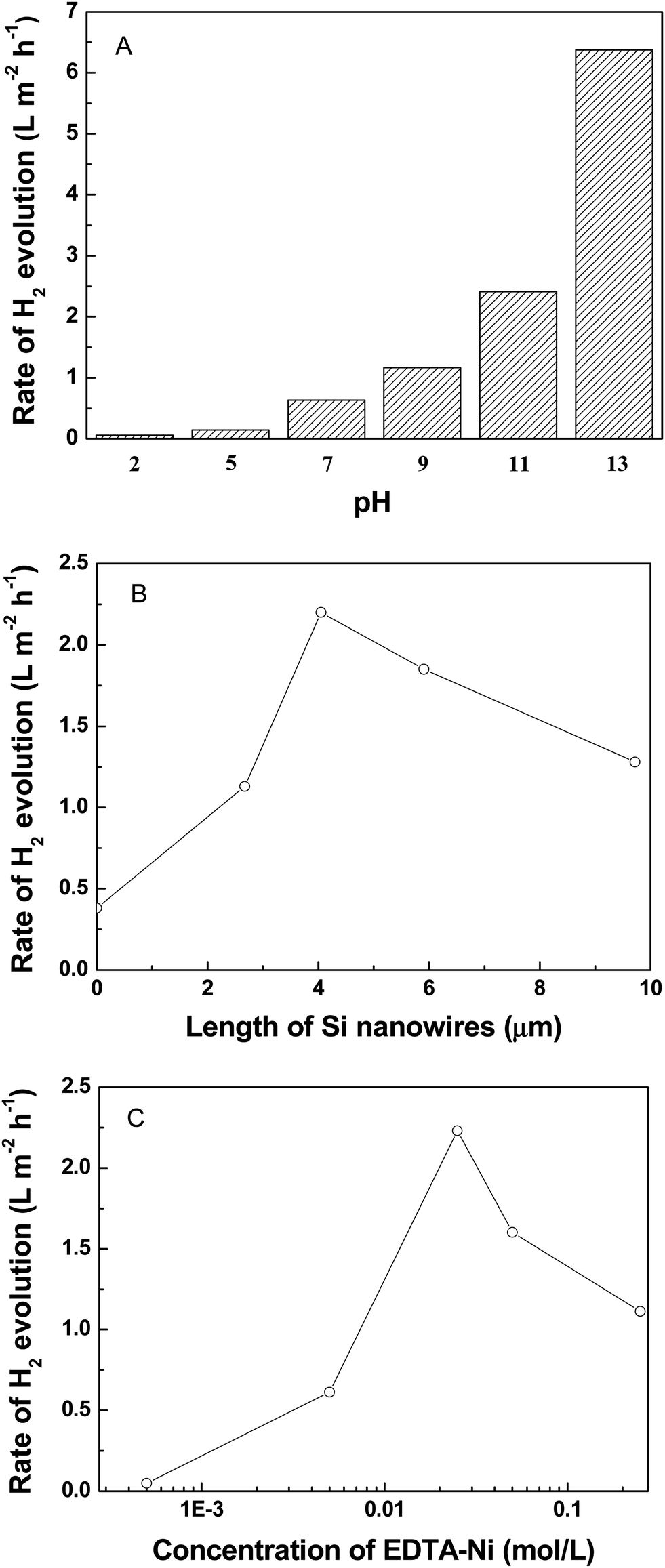 | ||
| Fig. 5 (A) Effect of pH on the photocatalytic activity of the EDTA-Ni sensitized SiNWs (SiNWs: 3 cm × 3 cm; length of nanowires: 4 μm; EDTA-Ni aqueous solution: 0.025 mol L−1 100 mL; irradiation time: 5 h); (B) effect of nanowires length on the photocatalytic activity of the EDTA-Ni sensitized SiNWs (SiNWs: 3 cm × 3 cm; EDTA-Ni aqueous solution: 0.025 mol L−1 100 mL; pH: 11; irradiation time: 5 h); (C) effect of concentration of EDTA-Ni on the photocatalytic activity of the EDTA-Ni sensitized SiNWs (SiNWs: 3 cm × 3 cm; length of nanowires: 4 μm; pH: 11; irradiation time: 5 h). | ||
Furthermore, ESI Fig. S2† shows the H2 evolution rate over SiNWs at various pH when EDTA-Na is used as a sacrificial reagent. As can be seen from Fig. S2,† the rate of hydrogen evolution over SiNWs decreases unilaterally with pH increasing, which is contrary to the photocatalytic behavior of SiNWs in the EDTA-Ni solution. In addition, the pH of the solution hardly changes during hydrogen evolution (ESI Fig. S3†). These phenomena indicate that the contribution from the reaction between silicon and basic solutions towards hydrogen evolution could be negligible in comparison with that due to the introduction of EDTA-Ni.
Fig. 5B shows the effect of the length of silicon nanowires on the photocatalytic activity of the EDTA-Ni sensitized SiNWs. From Fig. 5B, it can be observed that the rate of H2 evolution increases with the nanowires length increasing from 0 to 4 μm, and thereafter begins to decrease with increasing the nanowires length. The optimal nanowires length is 4 μm. One possible explanation is that the light absorption and the Si nanowires/electrolyte contact area would increase with the nanowires length increasing.13 In addition, the aspect ratio of Si wires would also increase with increasing the nanowires length. Higher aspect ratio is advantageous for the photon-generated carriers transfer, which leads to efficient separation of electron–hole pairs.29 Therefore, the photocatalytic activity of the EDTA-Ni sensitized SiNWs increases with the nanowires length increasing at the beginning. However, it will become more difficult that the tiny H2 bubbles leave from the surface of SiNWs when the nanowires length increases. Thus, the rate of H2 evolution gradually decreases with the nanowires length increasing from 4 μm to 9.7 μm.
Fig. 5C shows the effect of the concentration of EDTA-Ni on the rate of H2 evolution over the EDTA-Ni sensitized SiNWs. As can be seen from Fig. 5C, the rate of hydrogen evolution increases with the concentration of EDTA-Ni increasing from 5 × 10⁻⁴ mol L−1 to 0.025 mol L−1. Then the rate of hydrogen evolution decreases if the concentration of EDTA-Ni further increases. One possible explanation is that at the beginning, the light absorption of the system will increase with the dosage of EDTA-Ni increasing. However, the overdose of EDTA-Ni leads to decrease of effective absorption of the SiNWs. Thus, higher concentration of EDTA-Ni is not beneficial to the photocatalytic H2 evolution. Consequently, when the concentration of EDTA-Ni increases further beyond 0.025 mol L−1, the rate of hydrogen evolution decreases.
In order to test the repeatability of the EDTA-Ni sensitized SiNWs, the durability of the EDTA-Ni sensitized SiNWs was examined by repeated the H2 evolution for 3 cycles in the same conditions (Fig. 6). As can be seen from Fig. 6, no obvious deactivation of the EDTA-Ni sensitized SiNWs can be observed in the third cycle compared with the fresh catalyst. Because the dosage of EDTA-Ni is much more than the EDTA-Ni consumption, it is reasonable to assume that the concentration of EDTA-Ni is constant in the photocatalytic process. Therefore, we can conclude that the EDTA-Ni sensitized SiNWs is a stable and recyclable photocatalyst for photocatalytic H2 evolution.
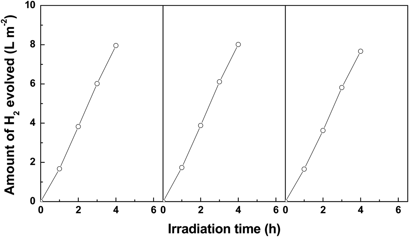 | ||
| Fig. 6 Durability of the EDTA-Ni sensitized SiNWs for the photocatalytic production of H2 (SiNWs: 3 cm × 3 cm; length of nanowires: 4 μm; EDTA-Ni aqueous solution: 0.025 mol L−1 100 mL; pH: 11). | ||
Conclusions
In summary, the EDTA-Ni sensitized SiNWs is an efficient cocatalyst-free photocatalyst for the photocatalytic H2 evolution under simulated sunlight irradiation. In the photocatalytic process, EDTA-Ni cannot be only an efficient sacrificial reagent, but also serve as an excellent sensitizer, which provide us with new possibility for finding a new photocatalyst for efficient H2 production driven by sunlight. Further efforts are currently being undertaken.Acknowledgements
This work was financially supported by the Open Project of Beijing National Laboratory for Molecular Sciences (No. 20140163), the Key Project of Science and Technology Innovation of Shanghai Education Commission (No. 13ZZ135) and the National Natural Science Foundation of China (No. 21301118).References
- T. Sreethawong and S. Yoshikawa, Catal. Commun., 2005, 6, 661 CrossRef CAS PubMed.
- J. Y. Zhang, Y. H. Wang, J. Zhang, L. Zhang, F. Huang and J. Yu, ACS Appl. Mater. Interfaces, 2013, 5, 1031 CAS.
- J. H. Byeon and Y.-W. Kim, ACS Appl. Mater. Interfaces, 2013, 5, 3959 CAS.
- S. Cao and J. Yu, J. Phys. Chem. Lett., 2014, 5, 2101 CrossRef CAS.
- N. Liu, C. Schneider, D. Freitag, M. Hartmann, U. Venkatesan, J. Muller, E. Spiecker and P. Schmuki, Nano Lett., 2014, 14, 3309 CrossRef CAS PubMed.
- M. Li, Y. Hu, S. Xie, Y. Huang, Y. Tong and X. Lu, Chem. Commun., 2014, 50, 4341 RSC.
- J. M. Thornton and D. Raftery, ACS Appl. Mater. Interfaces, 2012, 4, 2426 CAS.
- Z. Wang, S.-W. Cao, S. C. J. Loo and C. Xue, CrystEngComm, 2013, 15, 5688 RSC.
- P. Wang, P. Chen, A. Kostka, R. Marschall and M. Wark, Chem. Mater., 2013, 25, 4739 CrossRef CAS.
- M. Manikandan, T. Tanabe, P. Li, S. Ueda, G. V. Ramesh, R. Kodiyath, J. Wang, T. Hara, A. Dakshanamoorthy, S. Ishihara, K. Ariga, J. Ye, N. Umezawa and H. Abe, ACS Appl. Mater. Interfaces, 2014, 6, 3790 CAS.
- X. Li, W. Lu, W. Dong, Q. Chen, D. Wu, W. Zhou and L. Chen, Nanoscale, 2013, 5, 5257 RSC.
- X. Li, J. Li, T. Chen and H. Yu, Nanoscale Res. Lett., 2010, 5, 1721 CrossRef CAS PubMed.
- X. Qi, G. She, X. Huang, T. Zhang, H. Wang, L. Mu and W. Shi, Nanoscale, 2014, 6, 3182 RSC.
- J. Shi and X. Wang, Energy Environ. Sci., 2012, 5, 7918 CAS.
- Q. Ding, F. Meng, C. R. English, M. Caban-Acevedo, M. J. Shearer, D. Liang, A. S. Daniel, R. J. Hamers and S. Jin, J. Am. Chem. Soc., 2014, 136, 8504 CrossRef CAS PubMed.
- G. Yuan, H. Z. Zhao, X. H. Liu, Z. Hasanali, Y. Zou, A. Levine and D. Wang, Angew. Chem., Int. Ed., 2009, 48, 9680 CrossRef CAS PubMed.
- I. Oh, J. Kye and S. Hwang, Nano Lett., 2012, 12, 298 CrossRef CAS PubMed.
- C. Huang, Y. Lv, Q. Zhou, S.-Z. Kang, X. Q. Li and J. Mu, Ceram. Int., 2014, 40, 7093 CrossRef CAS PubMed.
- W. Kim, T. Tachikawa, T. Majima, C. H. Li, H. Kim and W. Y. Choi, Energy Environ. Sci., 2010, 3, 1789 CAS.
- L. J. Yu, X. H. Zhang, C. S. Zhuang, L. Lin, R. J. Li and T. Y. Peng, Phys. Chem. Chem. Phys., 2014, 16, 4106 RSC.
- M. C. Yin, S. Ma, C. J. Wu and Y. T. Fan, RSC Adv., 2015, 5, 1852 RSC.
- K. Maeda, M. Eguchi, S. A. Lee, W. J. Youngblood, H. Hata and T. E. Mallouk, J. Phys. Chem. C, 2009, 113, 7962 CAS.
- K. Maeda, M. Eguchi, W. J. Youngblood and T. E. Mallouk, Chem. Mater., 2009, 21, 3611 CrossRef CAS.
- J. Park, J. Yi, T. Tachikawa, T. Majima and W. Choi, J. Phys. Chem. Lett., 2010, 1, 1351 CrossRef CAS.
- A. M. Manke, K. Geisel, A. Fetzer and P. Kurz, Phys. Chem. Chem. Phys., 2014, 16, 12029 RSC.
- K. Peng, Y. Xu, Y. Wu, Y. Yan, S.-T. Lee and J. Zhu, Small, 2005, 1, 1062 CrossRef CAS PubMed.
- J.-Y. Jung, M. J. Choi, K. Zhou, X. Li, S.-W. Lee, H.-D. Um, M.-J. Park, K.-T. Park, J. H. Bang and J.-H. Lee, J. Mater. Chem. A, 2014, 2, 833 CAS.
- L. He, S.-Z. Kang, X. Li, L. Wang, L. Qin and J. Mu, Catal. Lett., 2015, 145, 1307 CrossRef CAS.
- X. Zhang, Y. Liu and Z. Kang, ACS Appl. Mater. Interfaces, 2014, 6, 4480 CAS.
Footnote |
| † Electronic supplementary information (ESI) available. See DOI: 10.1039/c5ra11248f |
| This journal is © The Royal Society of Chemistry 2015 |