
Cation exchange for thin film lead iodide perovskite interconversion†
Giles E.
Eperon
,
Clara E.
Beck
and
Henry J.
Snaith
*
Department of Physics, Clarendon Laboratory, University of Oxford, Oxford OX1 3PU, UK. E-mail: h.snaith1@physics.ox.ac.uk
First published on 2nd October 2015
Abstract
We report a new technique for tuning the bandgap of hybrid organic–inorganic halide perovskite materials. By dipping films of methylammonium or formamidinium lead triiodide (MAPbI3 or FAPbI3) in solutions of formamidinium or methylammonium iodide (FAI or MAI) at room temperature, we are able to inter-convert through cation exchange between perovskite materials, allowing us to carefully tune the bandgap between 1.57 and 1.48 eV. We observe uniform conversion through the entirety of the bulk film, with no evidence for a “bi-layered” or graded structure. By applying this technique to solar cell devices, we are able to enhance the performance of the single cation devices. Furthermore, we demonstrate that this technique allows us to form pure black phase FAPbI3 infiltrated into mesoporous scaffolds; this is normally infeasible since the pores confine the FAPbI3 in a yellow non-perovskite phase with a much wider bandgap, which is not of practical use in solar cells or other optoelectronic devices. Additionally, this work provides evidence for molecular cation mobility in the halide perovskites, indicating that the cations play a role in ionic conduction as well as the mobile anions.
Conceptual insightsHalide perovskite materials, solution-processable semiconductors with an ABX3 crystal structure, have recently become the subject of extreme interest for their use in photovoltaics and other optoelectronics. The best-performing perovskite material, formamidinium lead iodide (FAPbI3), is more difficult to process and requires higher temperatures than the more-studied wider bandgap methylammonium lead iodide (MAPbI3). In this work it is shown that bulk A-site cation exchange can take place in these films when immersed in a solution containing a suitable replacement cation, allowing conversion from MAPbI3 to the FAPbI3 (and in reverse) easily and at room temperature. Conversion takes place via crystalline mixed-cation intermediates, allowing fine tuning of the bandgap. Importantly, by converting from an already-formed perovskite, this process allows the formation of the formamidinium perovskite black phase in a mesoporous scaffold for the first time, a structure which has displayed good results for the methylammonium material but normally constrains the formamidinium material in a non-perovskite yellow phase. A second key insight is that despite the bulky size of the cation, the materials allow ion diffusion easily enough through the whole film to convert the film uniformly with no gradation. Furthermore, solar cells fabricated with mixed-cation materials made in this way show superior performance to the neat materials. |
Introduction
Hybrid organic–inorganic lead halide perovskite solar cells have recently attracted a lot of attention due to their meteoric rise in power conversion efficiencies, rising from 3.8% to over 20% in a matter of years.1–4 These materials show promise not only as solar cells but also as easily and cheaply fabricated semiconducting materials for LEDs, lasers and transistors.5–9The most widely studied organic–inorganic perovskite material, with a vast array of processing methods becoming prevalent, is methylammonium lead triiodide (MAPbI3).10 This perovskite has a bandgap of ∼1.57 eV and can be formed at low temperatures (∼100 °C). However, a number of recent reports have studied a new perovskite, formamidinium lead triiodide (FAPbI3). This perovskite has the same ABX3 structure as MAPbI3 but a narrower bandgap, achieved by replacing the methylammonium cation with a slightly larger formamidinium cation.2,11,12 It has a bandgap of ∼1.48 eV, closer to the single-junction solar cell optimum, but it requires temperatures of >150 °C to form the required perovskite phase, residing in a yellow non-perovskite phase at temperatures below this.13 In fact, the optimum composition for a perovskite solar cell may be a mixture of FAPbI3 and MAPbI3. By changing the ratio of MA and FA cations present, it has been shown that the bandgap can be tuned between that of MAPbI3 and FAPbI3, and that these mixed compositions have favourable properties in terms of structural stability in the black phase and performance.2,13,14
Cation exchange is a well-studied concept in the field of nanocrystals, for example the exchanges of Cu, Cd, Pb, In and Zn in nanocrystals has been demonstrated and is well-understood, often resulting in materials with properties superior to the initial parent material.15,16 After the synthesis of nanocrystals, they are exposed to a solution of the cation to be substituted, and over time the cation exchange occurs. It can be driven by a preferential chemical reaction or simple diffusion with mass action ensuring the desired conversion is achieved. It is most often used to retain the initial structure of a material whilst changing the composition to one which cannot easily be obtained straight from precursors. In bulk films, ionic exchange is less well studied. There has been some study on the insertion of halide anions into layered oxide perovskites.17 Most recently, Pellet and co-authors have reported the observation of rapid anion exchange in thin perovskite films, by exposing MAPbX3 (X = Cl, Br, I) to MAX solution. They observe that the halides are easily transported within the perovskite lattice, and that the morphology is generally preserved. However, there does not exist any study on whether transformation can occur in the same way between the larger organic cations.
First principles calculations suggest that both anions and molecular cations should be mobile species with low activation energy for migration (0.6 eV for I− and 0.8 eV for MA+), taking part in ionic conduction in the material, which suggests that cation exchange should be able to occur in a similar manner to the anion exchange.18
Herein we study the substitution of organic cations within the APbI3 perovskite structure (A = MA or FA). We expose an initial perovskite film of MAPbI3 or FAPbI3 to solutions containing a different cation (MAI or FAI) and use X-ray diffraction, absorption spectra, and photoluminescence to monitor conversion of the perovskite structure between MAPbI3 and FAPbI3. We find that on a time-scale of minutes, even quite thick films of perovskite, relevant for solar cells, can undergo conversion between perovskites, with mixed cation perovskites being formed in between. This allows us to overcome a previous limitation of the formamidinium based perovskite – forming it on a mesoporous scaffold, which previously has resulted in the yellow phase being formed, even with high temperature annealing. Furthermore, this provides a route for forming black phase FAPbI3 at lower temperatures than normally needed. We also find that the presence of the mesoporous scaffold, as was found for anion exchange,19 vastly accelerates the rate of perovskite inter-conversion. We fabricate solar cells with the converted perovskites, and show that in some cases we can enhance photovoltaic properties of the perovskite films by a simple dip treatment of the as-formed film.
Results and discussion
Initially we studied the conversion of MAPbI3 by FAI exposure, dissolved in propan-2-ol. We formed MAPbI3 films via the non-stoichiometric chloride precursor route, to give films of ∼400 nm thickness, which were subsequently dipped at room temperature in a dry atmosphere in 10 mg ml−1 FAI in propan-2-ol. After dipping for a certain time, films were rinsed with propan-2-ol and dried at 100 °C. As we show in Fig. 1a, we found that upon dipping the perovskite film into the solution, within tens of minutes the absorbance begins to red-shift towards the FAPbI3 absorption onset, with a gradual shift from the neat MAPbI3 absorption towards a reference sample of neat FAPbI3, with the conversion slowing after around 240 minutes. After a significantly longer time (840 min), the red shift ceases to progress further. This implies that we are converting MAPbI3 to FAPbI3via a cation exchange.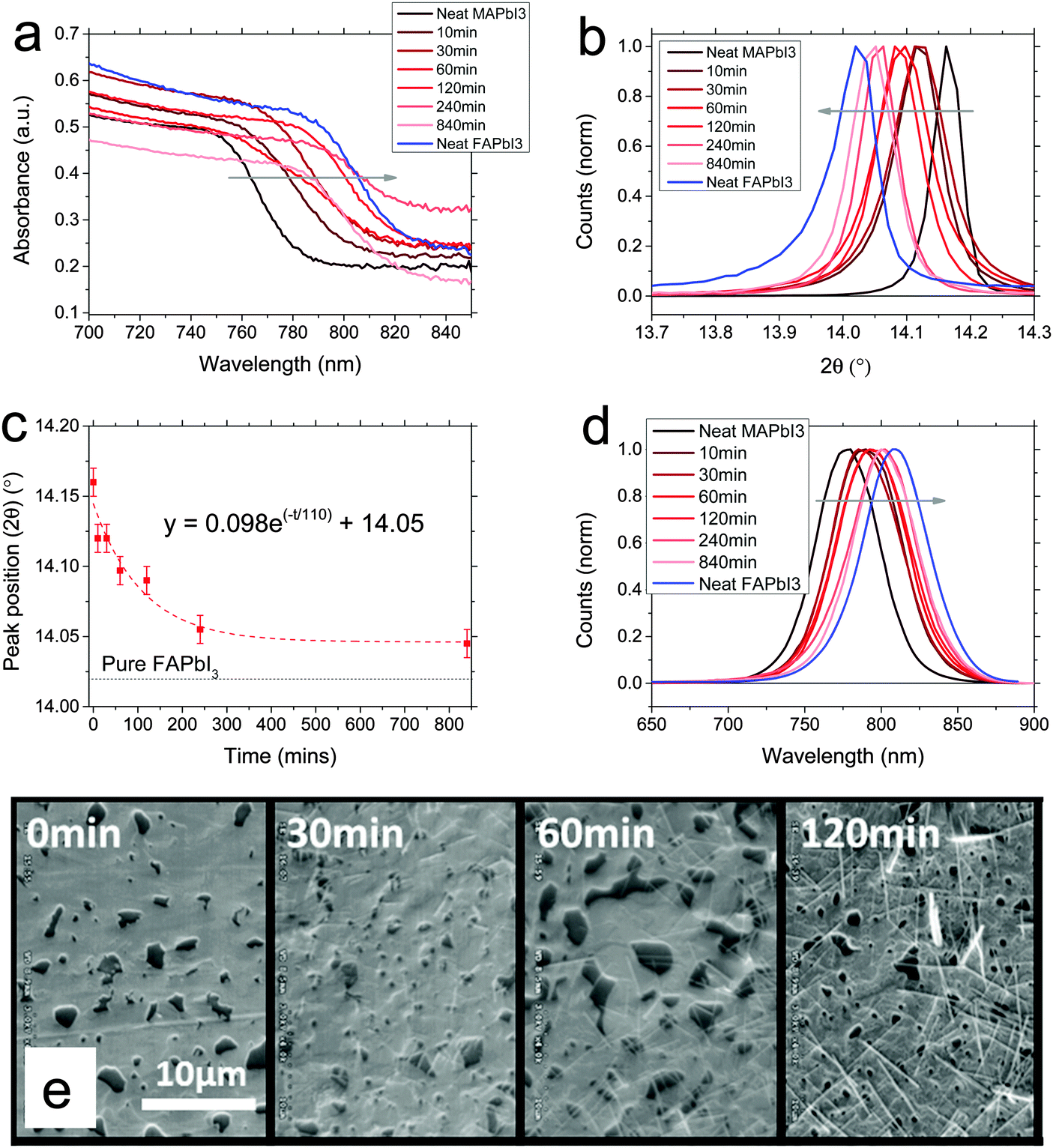 | ||
| Fig. 1 MAPbI3 conversion to FAPbI3·MAPbI3 films dipped in FAI solution for varying times. (a) Absorbance spectra showing onset of absorption. (b) Normalised X-ray diffraction spectra, magnified around 14°. (c) Plot of peak position against dipping time, fit with an exponential decay. (d) Normalised photoluminescence spectra. (e) Scanning electron micrographs of films dipped for different times. Scale is the same in all cases. | ||
We also show measured X-ray diffraction spectra in Fig. 1b. FAPbI3 (black phase) has been recently reported to have a cubic structure, whereas MAPbI3 has a tetragonal structure, at room temperature, the difference being a slight rotation of the lead iodide octahedra.20 However, these crystal structures are fundamentally very similar so would be likely to support intermixing and facile conversion between the two without much lattice stress. We show the full spectra in the ESI,† (Fig. S2); in Fig. 1b we show a magnification around the peak observed at ∼14°, which corresponds to the (110) peak of MAPbI3 tetragonal phase and the (100) peak of FAPbI3 cubic black phase. Here too we observe a continuous shift between the crystal structures. Importantly there is no time at which we do not observe a strongly crystalline material, which might be expected if we have too much lattice strain. This observation implies that we can easily substitute the cations throughout the lattice without detriment to the crystal structure. Moreover, we do not observe two distinct peaks in any case, which we would expect to observe if the film was segregated into MAPbI3 and FAPbI3 domains. Hence, the conversion must take place throughout the whole film and homogenise on the time scale of the experiment; the cations must easily move through the lattice. We note that even after 840 minutes, the peak is not completely shifted to the position of neat FAPbI3. As such, it appears that conversion is not 100% complete even after a very long time. This indicates that there is a thermodynamically stable point in the substitution of MA with FA, beyond which the reaction will not progress further. We also observe an emergence of a peak corresponding to the FAPbI3 yellow phase (see spectra in ESI†) at ∼11.8°, arising after 120 minutes. To estimate a rate of reaction, we plotted the position of the XRD peak at ∼14° as a function of time (Fig. 1c); by fitting with an exponential decay (as expected for a chemical substitution reaction) we extract a time constant of 110 minutes.19
We also measured photoluminescence (PL) of the converted films. All films exhibited strong photoluminescence. Here, we also observe a gradual transition from MAPbI3 PL to FAPbI3 PL spectra, in good agreement with the XRD and absorbance spectra, again indicating that the transition between perovskites occurs via fully crystalline mixed cation phases. In order to investigate the morphology, we took scanning electron micrographs, which we show in Fig. 1e, of representative films at different points during the conversion. Initially the MAPbI3 has a reasonably continuous morphology with large crystallites and a few large pinholes. As the conversion progresses, we observe little change in the macroscopic structure, but we do observe the formation of some needle-like crystals on the surface. The appearance of significant needle-like structures is coincident with the rise of peaks corresponding to the yellow phase in the XRD (see ESI†), so as proposed for a similar observation by Binek et al., we assign these to the yellow phase of FAPbI3.13 This is the preferred crystal habit of the yellow FAPbI3, and yellow FAPbI3 is the preferred phase at room temperature, so it may assume this phase and shape after a long enough time in the presence of a partial solvent (IPA) at room temperature.21
We next studied the opposite conversion: FAPbI3 to MAPbI3. We show data from the equivalent experiments in Fig. 2. Films were spin-coated from 1![[thin space (1/6-em)]](https://www.rsc.org/images/entities/char_2009.gif) :1 FAI:PbI2 solution with hydroiodic acid added before spin-coating, to enhance solubility and enable the formation of a smooth film, crystallised at 170 C for 10 minutes and then dipped in 10 mg ml−1 MAI in propan-2-ol, rinsing and drying as before after dipping for a certain time.11 The films are also about 400 nm in thickness. We observe in this case a blue-shift of the absorbance onset towards the MAPbI3 perovskite onset, again indicating a continuous tuning of the bandgap, and that we are able to convert the perovskite in the same way via cation exchange. Fig. 2b and c show the X-ray diffraction peak positions near 14° as a function of dipping time. We observe here, that we are also not able to fully convert the material to MAPbI3, with conversion getting closer to the reference data than was the case for the conversion to FAPbI3, but not totally reaching it. Fitting the peak position with an exponential fit again, we extract a time constant of 36 minutes.
:1 FAI:PbI2 solution with hydroiodic acid added before spin-coating, to enhance solubility and enable the formation of a smooth film, crystallised at 170 C for 10 minutes and then dipped in 10 mg ml−1 MAI in propan-2-ol, rinsing and drying as before after dipping for a certain time.11 The films are also about 400 nm in thickness. We observe in this case a blue-shift of the absorbance onset towards the MAPbI3 perovskite onset, again indicating a continuous tuning of the bandgap, and that we are able to convert the perovskite in the same way via cation exchange. Fig. 2b and c show the X-ray diffraction peak positions near 14° as a function of dipping time. We observe here, that we are also not able to fully convert the material to MAPbI3, with conversion getting closer to the reference data than was the case for the conversion to FAPbI3, but not totally reaching it. Fitting the peak position with an exponential fit again, we extract a time constant of 36 minutes.
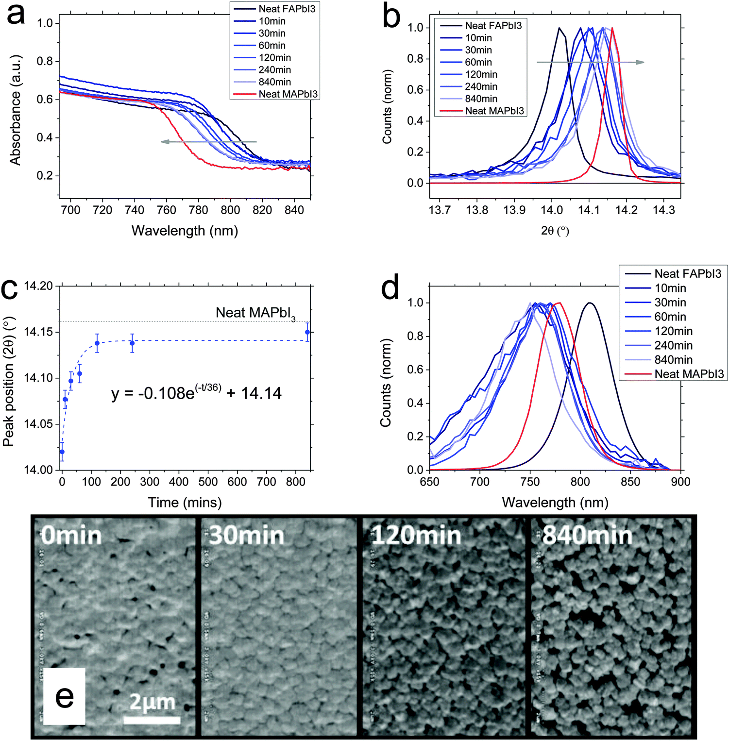 | ||
| Fig. 2 FAPbI3 conversion to MAPbI3·FAPbI3 films dipped in FAI solution for varying times. (a) Absorbance spectra showing onset of absorption. (b) Normalised X-ray diffraction spectra, magnified around 14°. (c) Plot of peak position against dipping time, fit with an exponential decay. (d) Normalised photoluminescence spectra. (e) Scanning electron micrographs of films dipped for different times. Scale is the same in all cases. | ||
Although the absorbance and XRD data show a continuous shift between FA and MA materials here, the photoluminescence spectra (Fig. 2d) behave in an unexpected manner. Upon dipping in MAI, instead of observing a blue-shift towards the MAPbI3 photoluminescence peak, the photoluminescence intensity immediately reduces and we observe it to be blue-shifted even further than the MAPbI3 spectrum, to ∼750 nm maximum. Longer dip time does not appear to change this. This is clearly in discrepancy to the absorbance and XRD spectra. Such blue-shifted photoluminescence, which is notably broader in energy than the PL peaks of either neat compounds, could arise from a strained perovskite phase, or some other structural disorder which increases the energetic disorder, where the broadening of sites occurs at higher energy than the band gap.22–25
In SEM images, as we show in Fig. 2e, here the morphology does significantly change in the conversion from FAPbI3 to MAPbI3. Starting as an apparently flat film of small crystallites, with a few pinholes, upon dipping, the film initially appears to become more uniform with pinholes closing, but we observe more crystal edges and the crystals appear to be re-orienting. On longer times, we observe a definite change in crystal orientation, appearing to form individual cuboid-like crystallites, but the re-orientation results in more pinholes being formed. This is likely due to the crystals being afforded some mobility by the propan-2-ol environment, in which the organic component is soluble. Over a long time, they are re-orienting to the preferred crystal shape and size of the MAPbI3. As discussed by Stoumpos et al., FAPbI3 and MAPbI3 have different crystal phases (for black phase FAPbI3) and hence different preferred crystal habit.21 MAPbI3 tends to an elongated rhombic dodecahedron but FAPbI3 a regular rhombic dodecahedron. This physical rearrangement of crystal shape appears to be responsible for the initial closing followed by eventual appearance of pinholes in the film. We propose that this may also be responsible for the blue-shifted PL, but much further work is required to understand the blue-shift in detail.
Having shown that we are able to convert between FAPbI3 and MAPbI3 flat films via cation exchange, we then turned to solving a unique problem of FAPbI3 deposition. If FAPbI3 is spin-coated straight onto a mesoporous scaffold (thicker than ∼200 nm), we find that it does not form the black α-phase even on heating at high temperatures, as it does in a thin solid film. It remains in the yellow δ-phase, appearing to be confined in that crystal structure by the scaffold (see ESI,† Fig. S1, for details). Mesostructured perovskite cells remain heavily investigated and may prove to be an important architecture, whether mesoporous TiO2 or mesoporous alumina are employed. We note that a thin mesoporous layer, with a thick capping layer of perovskite on top, is able to form the black phase; it is when the perovskite is significantly infiltrated into a scaffold that we observe the inhibition of black phase formation.2,12 Thus, if we can form MAPbI3 infiltrated into a mesoporous scaffold and then convert it into black phase FAPbI3via this interconversion approach, we could have a route to forming infiltrated black FAPbI3 perovskite. Since FAPbI3 has a lower bandgap than MAPbI3, the conversion of MAPbI3 to FAPbI3 in a mesoporous scaffold, where we retain the same crystal shape and size due to the constraints of the pores, should exhibit higher short-circuit current and hence performance. To test whether this is possible, we carried out the same dip-conversion on MAPbI3 film infiltrated within mesoporous alumina of ∼400 nm thickness.
We show absorbance of interconverted mesoporous-infiltrated MAPbI3 films in Fig. 3a, compared to a reference of planar FAPbI3. We observe that after much shorter times than for the planar films, the absorbance onset shifts towards the FAPbI3 onset. Within 30 minutes of dipping time, the onset is at the same place as the FAPbI3 onset, indicating that almost full conversion has occurred. However, the total absorbance in this region of the spectrum drops beyond 10 minutes of dipping time, indicating that there is likely some degradation or phase conversion happening. A magnification of the XRD spectra around 14° shows that we do achieve very nearly full conversion from MAPbI3 to black phase FAPbI3, and we note that the peak narrows as dip time progresses. This indicates that crystallite size is increasing; by 60 minutes it is almost as narrow as the planar FAPbI3 spectrum. This suggests that the perovskite is no longer being confined by the mesoporous scaffold (which limits crystallites to ∼50 nm). To further investigate what is occurring, we plot the XRD spectra on a larger 2θ scale, showing a peak associated with the yellow δ-phase at 11.8°. We observe that after ∼30 minutes, a significant (compared to the black phase peak) amount of yellow phase FAPbI3 becomes apparent. We thus propose that over time, in propan-2-ol, which is a partial solvent, the perovskite rearranges to form yellow phase crystals on top of the mesoporous scaffold, rather than inside it. These crystals are no longer confined by the mesoporous scaffold and hence form larger crystallites than those confined by the scaffold. We fitted an exponential decay to the ∼14° peak position over time, and find a good fit with a time constant (τ) of 14.7 minutes. Compared to the conversion of planar films (τ ∼ 117 minutes), this is much faster.
 | ||
| Fig. 3 MAPbI3 conversion to FAPbI3 in a mesoporous scaffold. (a) Absorbance spectra showing onset of absorption. (b) Normalised X-ray diffraction spectra, magnified around 14°. (c) Magnification of XRD spectra around a larger region, showing the yellow δ-phase region. (d) Plot of peak position against dipping time, fit with an exponential decay. | ||
We can thus make some conclusions about the dynamics of the interconversion reaction. Firstly, the presence of a mesoporous scaffold accelerates the reaction – comparing MAPbI3 conversion we observe a τ of 14.7 rather than 117 minutes. Presumably the larger surface area of perovskite infiltrated into the mesoporous scaffold facilitates a faster reaction. This is in good keeping with the observations of Pellet et al., who observed a similar process with anion exchange.19 Secondly, we observe that for similar thickness planar films, the reaction from FAPbI3 to MAPbI3 is faster than vice versa, with τ of 36 rather than 117 minutes. Whilst we note that the differing morphologies of the two perovskite films are likely to have an effect, this could also be due to the reaction favouring an energetically preferred configuration. In this case, this would imply that the MAPbI3 perovskite is energetically more favourable than FAPbI3. As recently pointed out by Binek et al., the interaction of the MA cation with the lead iodide lattice is stronger than the FA cation, since it has a greater dipole moment (2.3D compared to 0.21D).26 This means that stronger hydrogen bonds to the iodide ions will be formed in MAPbI3 than FAPbI3, making it a more energetically favourable lattice. The conversion to FAPbI3 will still be driven by the vast excess of FA cations in the solution, but more slowly than the equivalent MA reaction. In all cases, almost total conversion is achieved, with no bi-layer perovskites being formed. As such, the mobility of cations throughout the perovskite lattice must be rapid and facile. This observation suggests that the assertion of Lee and co-workers, that by spin-coating MAI in propan-2-ol on top of FAPbI3 they could form a layer of MAPbI3 as a discrete layer on top of FAPbI3, is likely to be incorrect.12 This technique is analogous to the dip-conversion and we never observe two distinct crystal structures for MAPbI3 and FAPbI3.
Having demonstrated the conversion between different perovskites, we fabricated solar cells in order to investigate the impact of this conversion on devices. We note that there are several effects at play in the conversion reactions; as well as the conversion from one perovskite to another, we have the introduction of strain on the lattice, the changing morphology of the planar films, and the degradation into the yellow FAPbI3 phase at long dipping times.
We fabricated planar solar cells in the architecture FTO/compact TiO2/perovskite/spiro-OMeTAD/Au, and mesoporous solar cells with the same architecture but with a layer of mesoporous alumina deposited prior to the perovskite deposition. We deposited the perovskites layers as for the fabrication of films. We show current–voltage characteristics for champion devices, and average PCEs for the batch, at each dipping time in Fig. 4. We note that these devices did display current–voltage hysteresis, and stabilised PCEs are shown in the ESI,† (Fig. S4–S6). Considering first the MAPbI3 to FAPbI3 interconversion (Fig. 4a and b), we observe that for the first 2 hours, performance monotonically decreases slightly, mainly due to a reduction in Voc, and after that both Jsc and Voc are reduced significantly leading to poorly-performing devices for the longest dipping times. Though there is some evidence for a small increase in Jsc between 0 and 30 min, as we might expect for a narrower bandgap material, the performance is dominated by the reduction in Voc so there is no net gain in efficiency. Gradual formation of the yellow phase FAPbI3 needle structures is likely to be the cause of the dramatic drop in performance at long conversion times.
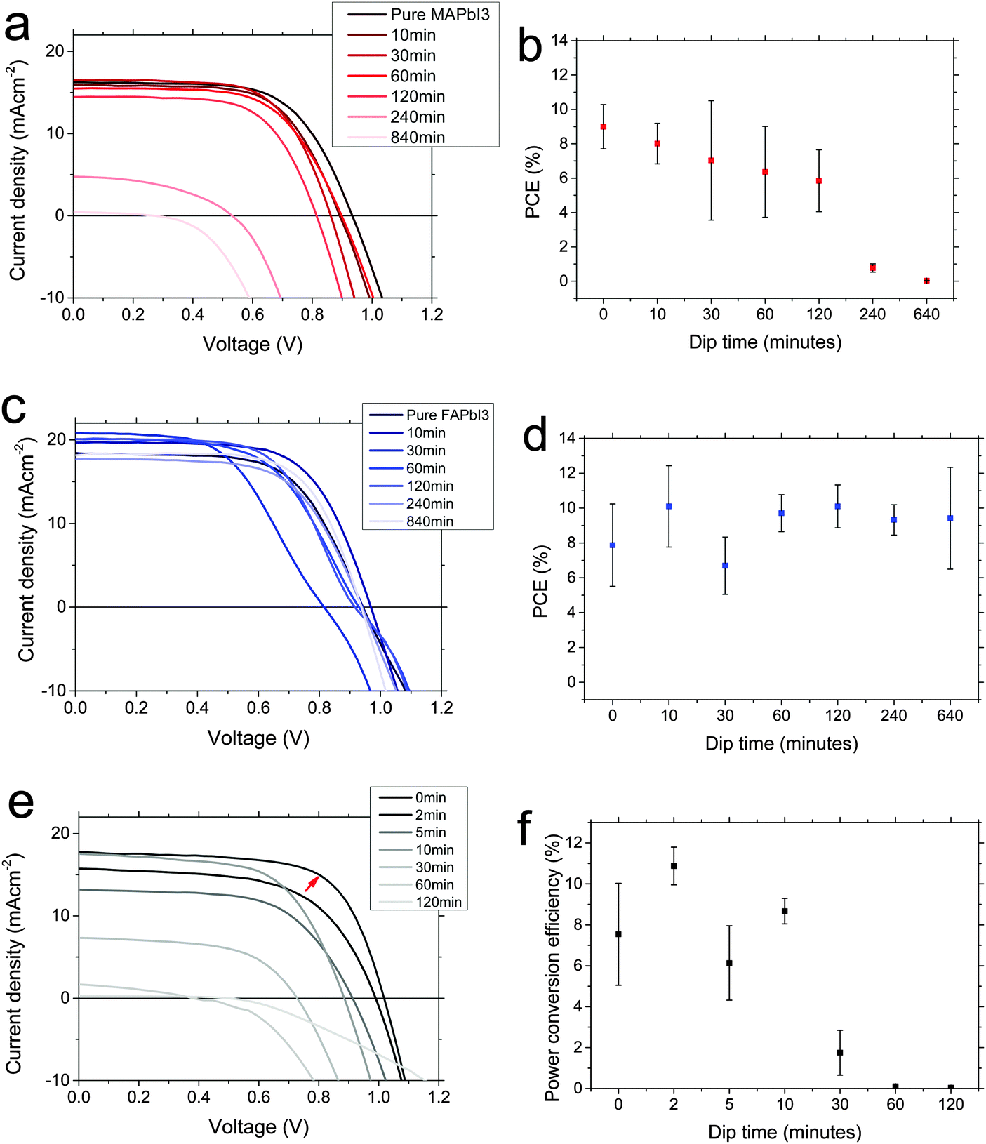 | ||
| Fig. 4 Solar cell characteristics of interconverted perovskite solar cells. Current–voltage characteristics measured under AM1.5 illumination for (a) MAPbI3 conversion to FAPbI3 (planar), (c) FAPbI3 to MAPbI3 (planar) and (e) MAPbI3 to FAPbI3 on mesoporous alumina scaffolds. Average fast-scanned PCE determined from J–V curves is shown in (b), (d), and (f) respectively. Devices were held at 1.4 V for 5 s before measuring, and measured from 1.4 V to 0 V at 0.38 V s−1. Average data is taken from at least 7 devices per point. | ||
Considering then the FAPbI3 to MAPbI3 interconversion (Fig. 4c and d), we observe that upon dipping for 10 minutes or more, the PCE increases (except for an apparently anomalous 30 minute dipping result). This is due mainly to an increase in short-circuit current. We note that this is not entirely expected; a wider bandgap material (MAPbI3) should produce less current. However, looking more closely, we note that at 10 minutes the bandgap has not shifted much (Fig. 2a and b), but looking at the SEM images (Fig. 2e), the film becomes more continuous, with fewer pinholes. This will also have the effect of increasing short-circuit current, simply because there are fewer regions where light can pass straight through. We propose that this morphological effect, rather than any intrinsic electronic material property, is dominating the solar cell performance change. The performance begins to drop again at the later dipping times, and this is in keeping with the again reduced uniformity of the perovskite film. We note that the unexpectedly blue-shifted PL has no obvious detrimental effect on device performance here.
Finally, we consider the mesoporous devices, converted from MAPbI3 to FAPbI3. Upon short dipping times, up to ∼5–10 minutes, we observe higher PCE. In particular, for this batch a 2 minute dip shows significantly improved PCE. We note that more experimental data would be necessary to conclude the optimum ‘perfect’ dipping time, due to the variation between 2, 5 and 10 minutes points. This full optimisation is beyond the scope of this study, however – here we conclude that a short dipping time is able to give rise to higher PCE. Upon longer dipping times, performance drops off critically and by 30 minutes it is very poor. The improvement observed at short dip times comes mainly from an enhanced short-circuit current. Since at 10 minutes, we do observe a significant shift in material bandgap to a narrower value (Fig. 3), it is likely that this is likely responsible for the short-circuit current improvement; morphology plays less of a role in mesostructured devices. At longer dip times however, the performance drops off again, corresponding to production of the yellow FAPbI3 phase which we observed in Fig. 3.
As such we can conclude that for solar cell devices, whilst morphological and phase change effects play a crucial role in determining device performance, we are able to employ interconversion via dipping in MAI or FAI in propan-2-ol to fabricate higher performing devices. The optimum compositions appear to be somewhere in between MAPbI3 and FAPbI3 in the cases where we observe an improvement in device performance; this is in keeping with recent reports on the highest efficiency perovskite devices.2
FAPbI3 normally requires heating at high temperatures (>150 °C) to form the black phase. While we note that we do form some yellow phase, we are able to form FAPbI3 black phase by simply dipping a MAPbI3 film at room temperature in a solution of FAI, rinsing in propan-2-ol, and drying at 100 °C. This therefore reduces the fabrication temperature of a FAPbI3 film. While planar solar cells do not show improvements, due to morphological considerations and the production of some yellow phase, this technique may be able to be further optimised to lead to improvements, and could be of use in the field of lasers and LEDs. Moreover, while it is normally infeasible to form black phase FAPbI3 infiltrated in a mesostructured scaffold architecture, we have demonstrated that by inter-converting from infiltrated MAPbI3 we can form this. Whilst our solar cells do not perform well due to detrimental formation of some yellow phase, with further optimisation this could be of use in such devices. Most impressively, the material made by incomplete interconversion, a mixture of FAPbI3 and MAPbI3 (MAxFA1−xPbI3) shows improved solar cell performances compared to either neat phase. This implies that by a simple and quick dipping treatment we can enhance solar cell properties, and this may lead the way towards even higher efficiencies in the future.
An important aspect of this work is that it demonstrates strong evidence for high mobility of molecular cations in these materials. As reported by several groups recently, these perovskite materials appear to be good ionic conductors, but it was not known which species were moving – it was assumed to be predominantly the halide anions.18,27 However, it was also reported via first principles calculations that the activation energy for migration of the MA+ species would be just 0.2 eV more than the I− species, indicating that cation mobility is also probably high.18 Here, we observe comprehensive replacement of cations in the perovskite material, though at a slower rate than the anion exchange reported by others.19 This suggests that the cations are indeed easily mobile, though less so than the anions, in good agreement with the higher activation energy predicted. Ionic conduction in perovskites is thus likely to involve both anions and molecular cations, with higher mobility for the anions.
Conclusion
We have demonstrated that by dipping a film of FAPbI3 or MAPbI3 in MAI or FAI respectively, dissolved in propan-2-ol, organic cation exchange occurs, allowing us to convert almost fully between perovskites. We observe a transformation of the bulk material rather than formation of a bi-layered or graded structure. During conversion, we form crystalline intermediate phases of MAxFA1−xPbI3. This allows us to carefully tune the bandgap of this perovskite between 1.57 eV and 1.48 eV, having application in solar cells, and light emitting applications. Besides simply tuning the bandgap, we observe critical influences on changing the morphology and formation of yellow phase FAPbI3. Despite this, we are able to significantly enhance the performance of hybrid perovskite solar cells made of pure phase materials by exposing them to this simple dip-interconversion process. Importantly, this work provides good evidence for molecular cation mobility in the halide perovskites, indicating that ionic conduction in these materials likely involves both anions and molecular cations.Experimental
Materials
Unless otherwise stated, all materials were purchased from Sigma-Aldrich or Alfa Aesar and used as received. Spiro-OMeTAD was purchased from Borun Chemicals.Perovskite film fabrication
Formamidinium iodide (FAI) and methylammonium iodide (MAI) were synthesised in-house according to reported procedures.3,11To form the FAPbI3 precursor solution, FAI and PbI2 were dissolved in anhydrous N,N-dimethylformamide (DMF) in a 1:1 molar ratio, at 0.55 M of each reagent. Immediately prior to spin-coating, 38 μl of hydroiodic acid (57% w/w) was added to 1 ml of the 0.55 M precursor solution to enable smooth and continuous film formation.11 To form films, the precursor was then spin-coated in a nitrogen-filled glovebox at 2000 rpm, then annealed at 170 °C in air for 10 minutes.
To form the MAPbI3 precursor solution, methylammonium iodide and PbCl2 were dissolved in DMF in a 3:1 molar ratio, at 0.88 M PbCl2 and 2.64 M MAI. To form films, the precursor was spin-coated at 2000 rpm in a nitrogen-filled glovebox, allowed to dry at room temperature in the glovebox for 30 minutes, then annealed at 90 °C for 150 minutes followed by 120 °C for 15 minutes in the glovebox.
Films for optical studies were fabricated on plasma-cleaned microscope glass slides. For solar cells, films were fabricated on fluorine-doped tin oxide (FTO) coated glass (Pilkington, 7 Ω □−1). Initially FTO was removed from regions under the anode contact by etching the FTO with 2 M HCl and zinc powder. Substrates were then cleaned sequentially in hallmanex detergent, acetone, propan-2-ol and oxygen plasma.
Inter-conversion
For the dip-interconversion, films were immersed in solutions of MAI or FAI in propan-2-ol in a nitrogen-filled glovebox at a concentration of 10 mg ml−1 for varying times. After dipping, films were rinsed in propan-2-ol and then dried at 100 °C for 30 minutes.Device fabrication
A ∼50 nm hole-blocking layer of compact TiO2 was first deposited by spin-coating a mildly acidic solution of titanium isopropoxide in ethanol (350 μl in 5 ml ethanol with 0.013 M HCl) at 2000 rpm, and annealed at 500 °C for 30 minutes. For the mesoporous cells, 400 nm mesoporous alumina was then deposited by spin-coating at 2500 rpm a solution of 20 nm alumina nanoparticles suspended in propan-2-ol, which was then dried at 150 °C. Here, the perovskite was deposited as before but spin-coated and annealed in air at 100 °C for 120 minutes.Following interconversion, the hole-transporting layer was then deposited via spin-coating a 0.0788 M solution in chlorobenzene of 2,2′,7,7′-tetrakis-(N,N-di-p-methoxyphenylamine)9,9′-spirobifluorene (spiro-OMeTAD), with additives of 0.0184 lithium bis(trifluoromethanesulfonyl)imide (added in 0.61 M acetonitrile solution) and 0.0659 M 4-tert-butylpyridine. Spin-coating was carried out at 2000 rpm.
Gold electrodes were then thermally evaporated under vacuum of ∼10−6 Torr, at a rate of ∼0.1 nm s−1, to complete the devices.
Device characterisation
The current density–voltage (J–V) curves were measured (2400 Series SourceMeter, Keithley Instruments) under simulated AM 1.5 sunlight at 100 mW cm−2 irradiance generated by an Abet Class AAB sun 2000 simulator, with the intensity calibrated with an NREL calibrated KG5 filtered Si reference cell. The mismatch factor was calculated to be 1.2% between 400 and 1100 nm. The solar cells were masked with a metal aperture to define the active area, which was 0.0919 cm−2, and measured in a light-tight sample holder to minimize any edge effects.Optical measurements
Absorbance spectra were collected with a Varian Cary 300 UV-Vis spectrophotometer with an internally coupled integrating sphere.Materials characterization
A Hitachi S-4300 field emission scanning electron microscope was used to acquire SEM images. Sample thicknesses were measured using a Veeco Dektak 150 surface profileometer. X-ray diffraction spectra were obtained using a Panalytical X'Pert Pro X-ray diffractometer.Photoluminescence measurements
Steady-state PL measurements were acquired using a FluoTime 300 (PicoQuant GmbH) system. Film samples were photoexcited using a 510 nm laser head (LDH-P-C-510). The PL was collected using a high resolution monochromator and hybrid photomultiplier detector assembly (PMA Hybrid 40, PicoQuant GmbH).Acknowledgements
This work was part funded by EPSRC and from the European Union Seventh Framework Programme [FP7/2007-2013] under grant agreement no. 604032 of the MESO project. GE was supported by the EPSRC and Oxford Photovoltaics Ltd through a Nanotechnology KTN CASE award. CB was supported by Zühlke Engineering AG. We thank Jin Zhang and Martina Congiu for cleanroom maintenance and materials synthesis.References
- A. Kojima, K. Teshima, Y. Shirai and T. Miyasaka, Organometal Halide Perovskites as Visible-Light Sensitizers for Photovoltaic Cells, J. Am. Chem. Soc., 2009, 131, 6050–6051 CrossRef CAS PubMed
.
- N. J. Jeon, J. H. Noh, W. S. Yang, Y. C. Kim, S. Ryu, J. Seo and S. Seok II, Compositional Engineering of Perovskite Materials for High-Performance Solar Cells, Nature, 2015, 517, 476–480 CrossRef CAS PubMed
- M. M. Lee, J. Teuscher, T. Miyasaka, T. N. Murakami and H. J. Snaith, Efficient Hybrid Solar Cells Based on Meso-Superstructured Organometal Halide Perovskites, Science, 2012, 338, 643–647 CrossRef CAS PubMed
- NREL, Best Research-Cell Efficiencies, http://www.nrel.gov/ncpv/images/efficiency_chart.jpg, 2015.
- F. Deschler, M. Price, S. Pathak, L. Klintberg, D. D. Jarausch, R. Higler, S. Huettner, T. Leijtens, S. D. Stranks, H. J. Snaith, M. Atature, R. T. Phillips and R. H. Friend, High Photoluminescence Efficiency and Optically-Pumped Lasing in Solution-Processed Mixed Halide Perovskite Semiconductors, J. Phys. Chem. Lett., 2014, 5, 1421–1426 CrossRef CAS PubMed
- B. R. Sutherland, S. Hoogland, M. M. Adachi, C. T. O. Wong and E. H. Sargent, Conformal Organohalide Perovskites Enable Lasing on Spherical Resonators, ACS Nano, 2014, 8, 10947–10952 CrossRef CAS PubMed
- Z.-K. Tan, R. S. Moghaddam, M. L. Lai, P. Docampo, R. Higler, F. Deschler, M. Price, A. Sadhanala, L. M. Pazos, D. Credgington, F. Hanusch, T. Bein, H. J. Snaith and R. H. Friend, Bright Light-Emitting Diodes Based on Organometal Halide Perovskite, Nat. Nanotechnol., 2014, 9, 1–6 CrossRef PubMed
- Y. Mei, O. D. Jurchescu, C. Zhang and Z. V. Vardeny, Electrostatic Gating of Hybrid Halide Perovskite Field-Effect Transistors: Balanced Ambipolar Transport at Room-Temperature, MRS Commun., 2015, 1–5 Search PubMed
- X. Y. Chin, D. Cortecchia, J. Yin, A. Bruno and C. Soci, Lead Iodide Perovskite Light-Emitting Field-Effect Transistor, 2015 Search PubMed
- L. Zheng, D. Zhang, Y. Ma, Z. Lu, Z. Chen, S. Wang, L. Xiao and Q. Gong, Morphology Control of the Perovskite Films for Efficient Solar Cells, Dalton Trans., 2015, 44, 10582–10593 RSC
- G. E. Eperon, S. D. Stranks, C. Menelaou, M. B. Johnston, L. M. Herz and H. J. Snaith, Formamidinium Lead Trihalide: A Broadly Tunable Perovskite for Efficient Planar Heterojunction Solar Cells, Energy Environ. Sci., 2014, 7, 982–988 CAS
- J.-W. Lee, D.-J. Seol, A.-N. Cho and N.-G. Park, High-Efficiency Perovskite Solar Cells Based on the Black Polymorph of HC(NH2)2PbI3, Adv. Mater., 2014, 26, 4991–4998 CrossRef CAS PubMed
- A. Binek, F. C. Hanusch, P. Docampo and T. Bein, Stabilization of the Trigonal High Temperature Phase of Formamidinium Lead Iodide, J. Phys. Chem. Lett., 2015, 6, 1249–1253 CrossRef CAS PubMed
- N. Pellet, P. Gao, G. Gregori, T.-Y. Yang, M. K. Nazeeruddin, J. Maier and M. Grätzel, Mixed-Organic-Cation Perovskite Photovoltaics for Enhanced Solar-Light Harvesting, Angew. Chem., Int. Ed., 2014, 53, 3151–3157 CrossRef CAS PubMed
- L. De Trizio, M. Prato, A. Genovese, A. Casu, M. Povia, R. Simonutti, M. J. P. Alcocer, C. D. Andrea, F. Tassone and L. Manna, Strongly Fluorescent Quaternary Cu–In–Zn–S Nanocrystals Prepared from Cu 1 – X InS 2 Nanocrystals
by Partial Cation Exchange, Chem. Mater., 2012, 24, 2400–2406 CrossRef CAS
- H. Li, R. Brescia, R. Krahne, G. Bertoni, M. J. P. Alcocer, C. D'Andrea, F. Scotognella, F. Tassone, M. Zanella, M. De Giorgi and L. Manna, Blue-UV-Emitting ZnSe(Dot)/ZnS(Rod) Core/shell Nanocrystals Prepared from CdSe/CdS Nanocrystals by Sequential Cation Exchange, ACS Nano, 2012, 6, 1637–1647 CrossRef CAS PubMed
- T. A. Kodenkandath, A. S. Kumbhar, W. L. Zhou and J. B. Wiley, Construction of Copper Halide Networks within Layered Perovskites. Syntheses and Characterization of New Low-Temperature Copper Oxyhalides, Inorg. Chem., 2001, 40, 710–714 CrossRef CAS PubMed
- C. Eames, J. M. Frost, P. R. F. Barnes, B. C. O'Regan, A. Walsh and M. S. Islam, Ionic Transport in Hybrid Lead Iodide Perovskite Solar Cells, Nat. Commun., 2015, 6, 7497 CrossRef CAS PubMed
- N. Pellet, J. Teuscher, J. Maier and M. Grätzel, Transforming Hybrid Organic Inorganic Perovskites by Rapid Halide Exchange, Chem. Mater., 2015, 27, 2181–2188 CrossRef CAS
- M. T. Weller, O. J. Weber, J. M. Frost and A. Walsh, Cubic Perovskite Structure of Black Formamidinium Lead Iodide, Α-[HC(NH2)2]PbI3, at 298 K, J. Phys. Chem. Lett., 2015, 3209–3212 CrossRef CAS
- C. C. Stoumpos, C. D. Malliakas and M. G. Kanatzidis, Semiconducting Tin and Lead Iodide Perovskites with Organic Cations: Phase Transitions, High Mobilities, and Near-Infrared Photoluminescent Properties, Inorg. Chem., 2013, 52, 9019–9038 CrossRef CAS PubMed
- M. A. Schreuder, K. Xiao, I. N. Ivanov, S. M. Weiss and S. J. Rosenthal, White Light-Emitting Diodes Based on Ultrasmall CdSe Nanocrystal Electroluminescence, Nano Lett., 2010, 10, 573–576 CrossRef CAS PubMed
- C. Kisielowski, J. Krüger, S. Ruvimov, T. Suski, J. Ager, E. Jones, Z. Liliental-Weber, M. Rubin, E. Weber, M. Bremser and R. Davis, Strain-Related Phenomena in GaN Thin Films, Phys. Rev. B: Condens. Matter Mater. Phys., 1996, 54, 17745–17753 CrossRef CAS
- N. Thillosen, K. Sebald, H. Hardtdegen, R. Meijers, R. Calarco, S. Montanari, N. Kaluza, J. Gutowski and H. Lüth, The State of Strain in Single GaN Nanocolumns as Derived from Micro-Photoluminescence Measurements, Nano Lett., 2006, 6, 704–708 CrossRef CAS PubMed
- O. Schmidt and K. Eberl, Multiple Layers of Self-Asssembled Ge/Si Islands: Photoluminescence, Strain Fields, Material Interdiffusion, and Island Formation, Phys. Rev. B: Condens. Matter Mater. Phys., 2000, 61, 13721–13729 CrossRef CAS
- J. M. Frost, K. T. Butler, F. Brivio, C. H. Hendon, M. van Schilfgaarde and A. Walsh, Atomistic Origins of High-Performance in Hybrid Halide Perovskite Solar Cells, Nano Lett., 2014, 14, 2584–2590 CrossRef CAS PubMed
- T.-Y. Yang, G. Gregori, N. Pellet, M. Grätzel and J. Maier, The Significance of Ion Conduction in a Hybrid Organic-Inorganic Lead-Iodide-Based Perovskite Photosensitizer, Angew. Chem., Int. Ed., 2015, 54, 7905–7910 CrossRef CAS PubMed
Footnote |
| † Electronic supplementary information (ESI) available. See DOI: 10.1039/c5mh00170f |
| This journal is © The Royal Society of Chemistry 2016 |