
 Open Access Article
 This Open Access Article is licensed under a Creative Commons Attribution-Non Commercial 3.0 Unported Licence
Transfer and control of the orientation of 3D nanostructures fabricated by nanoskiving†
Zhiyuan
Zhao
a,
Ziwei
Zhou
b,
Gang
Zhang
*b and
Ryan C.
Chiechi
 *a
*a
aStratingh Institute for Chemistry and Zernike Institute for Advanced Materials, University of Groningen, Groningen 9747AG, The Netherlands. E-mail: r.c.chiechi@rug.nl
bState Key Lab of Supramolecular Structure and Materials, College of Chemistry, Jilin University, Changchun 130012, P. R. China. E-mail: gang@jlu.edu.cn
First published on 7th July 2016
Abstract
This communication describes the transfer and stacking of slabs of epoxy containing nanostructures fabricated by nanoskiving. Removal of the sacrificial layer and epoxy matrices produces 3D nanostructures via control over the position and alignment of each sequential layer. The process uses mild etchants and transfers the nanoskived features without wrinkling or damage. We demonstrate the utility of this method of transfer with aligned and intersecting nanowires and arrays of nano-holes and crescents.
Conceptual insightsThe core concept of this work is the drag and drop fabrication of 3D nanostructures by stacking slabs of epoxy embedded with nanostructures fabricated by nanoskiving. The fabrication is uncomplicated and can be utilized for rapid prototyping, deterministic and on-demand fabrication. What you see is what you get; there are no cropped micrographs hiding defects, low-yielding steps or other hidden complexities. The fabrication is mix-and-match in that disparate structures from different blocks can be stacked to form otherwise inaccessible nanostructures. We fabricate millimeter-long nanowires with control over the position, rotation and height, meaning meshes, grids, lines, etc. that can be formed on a surface, on top of other nano-objects or suspended such that the available surface area of the nano-structure is controllable. The accessible structures are sufficiently large in two dimensions to interact with micro- and milli-meter scale objects such as cells and are demonstrably useful for optical applications. This is an enabling technology for us and we think it will serve the same purpose for others. The key is the simplicity and accessibility of the entire fabrication scheme. It requires only a thermal evaporator and an ultramicrotome. Yet the scope of the possible structures and combination of materials is potentially very broad. |
Introduction
Nanoscience exploits the unique properties of nanoscale structures not found in bulk materials, requiring nanostructures with specific geometries and the interactions of multiple structures in well-defined arrays. The more elements there are in a nanostructured system, however, the more challenging it is to create the desired geometry. Thus, fabrication requires manipulating and addressing nanostructures individually and/or in ensembles and interfacing them with the macro world. A particularly challenging configuration is heterostructures that are stacked vertically (that is, three-dimensional fabrication). The fabrication of these devices requires the controlled transfer of ensembles of nanostructures from the substrate on which they are prepared to a target substrate with control over orientation without affecting the previously transferred structures.1,2 Existing methods for transferring nanostructures have focused mainly on transfer printing,3–7 and the transfer of two-dimensional materials such as graphene8–11 and MoS2.12–14 Transfer printing utilizes an elastomeric stamp as a mediator for the heterogeneous integration of nanostructures from a source substrate to a target surface. However, multiple transfer steps are difficult because the stamp must adhere to a structure on the source substrate and release it to the target without perturbing previously transferred structures. To separate the stamp from the target surface, chemical adhesion must be controlled while optimizing the pressing force. Additionally, the use of a stamp requires planar and hard source and target substrates. Free-standing films are an alternative for the transfer of polymer nano-sheets and inorganic, ultrathin layers.15–17 However, despite the substantial development of transfer methods, there is no robust, generalizable approach available for easily transferring, stacking and precisely manipulating nanostructures on surfaces.There are many approaches to fabricating nanostructures by various lithographic and self-assembly processes that immobilize nanostructures on as-prepared substrates into useful geometries. Conventional techniques for nanofabrication, such as electron beam lithography, focused-ion beam milling, photolithography, etc., can generate arbitrary patterns in materials to produce nanostructures. However, they require specialized facilities and are constrained by the limitations of planar lithography; they are not suitable for non-planar surfaces and have a low tolerance for organic materials, for example. Random assembly processes circumvent some of these limitations, but suffer from low yields and lack control over orientation.
Nanoskiving is a flexible technique for nanofabrication, which is a form of edge lithography based on sectioning thin structures with an ultramicrotome.18,19 It is facile, compatible with a wide variety of materials, including organics, and requires no special facilities or clean rooms. Nanostructures fabricated by nanoskiving are embedded in polymeric slabs that, after sectioning using a diamond knife, float in a water bath and can be collected simply by dipping virtually any substrate in the water. Although the nanostructures within each slab are precisely defined, there is no inherent control over the orientation of the slabs with respect to each other. Thus, after drying, the nanostructures are fixed arbitrarily on the substrate, precluding further manipulation or transfer.
There are two methods that afford some control over the orientation of the slabs before the water has evaporated. One is the direct, physical manipulation with, for example, a hair. A more sophisticated approach combines physical manipulation with alignment by magnetic fields.20 This latter method requires the embedding of nickel into the epoxy matrix along with the nascent nanostructures. The nickel then serves as a sacrificial ferromagnet that moors the entire epoxy slab to the magnetic field created by rare-earth magnets positioned below. This approach, therefore, requires that the materials of interest be incorporated alongside the nickel, which is co-embedded in the epoxy matrix and etched out in the last step (after sectioning, transfer and drying). To maximize the strength of the interaction with the external magnetic field, the dimensions of the nickel strips in the epoxy slabs should be as large as possible; however, a film that is too thick will damage the diamond knife. It is also necessary to slow the evaporation of the very small volume of water that supports the section during positioning, which must take place on a hydrophilic substrate to minimize capillary forces. Thus, when positioning successive sections, the epoxy matrix of the previous section (because it is hydrophobic) has to be removed. Thus, magnetic mooring is generally limited to relatively simple nanostructures (e.g., wires) and the positioning of one or two consecutive slabs. This technique also must take place in relatively close proximity to the microtome because the sections must remain floating on water between fabrication and positions. This is, of course, a common problem for any sort of nanofabrication that is highly dependent on equipment, regardless of the simplicity of that equipment.
This communication describes an on-demand transfer approach using a film of polymer as carrier layer and aluminum as sacrificial layer to transfer and manipulate sections that are fabricated by nanoskiving. Using this method, several sections can be prepared one-at-a-time and stored on a sacrificial surface. When the sections are needed, they can be transported and transferred onto a target substrate under ambient conditions. This transfer process is simple and fast and protects the nanostructures, keeping them intact and uniform without introducing defects, cracks, and residues. And no other materials (e.g., nickel for magnetic positioning) must be co-embedded. Positioning the sections does not depend on the wettability of substrates, which are not constrained in composition or topology. By successively stacking nanostructures (one-dimensional nanowires are used in this work), various two-dimensional (2D) or three-dimensional (3D) structures and even heterostructures can be constructed, improving the range of applications of nanoskiving. Virtually any structure fabricated by nanoskiving should be compatible with this “perfect transfer” method.
Experimental section
A 100 nm-thick gold film was deposited through a mask on a silicon wafer passivated with (tridecafluoro-1,1,2,2,-tetrahydrooctyl)trichlorosilane to form rectangular gold features before 8 mL of Epofix epoxy prepolymer was used to cover the entire wafer. After curing the epoxy for three hours at 60 °C, the gold layer was peeled off with the epoxy from the wafer so that the gold features remain adhered to the epoxy. The gold features were cut using a jeweler's saw into small pieces and placed into separate wells in a polyethylene microtome mold, which was then filled with more epoxy prepolymer, and cured for three hours at 60 °C to form epoxy blocks. A prepared block was placed in the ultramicrotome (Leica EM UC-7), and its top was trimmed to the width of the diamond knife (4 mm Diatome Ultra 35°) in a trapezoid shape using a razor blade. The block was first pre-cut with the ultramicrotome using a glass knife to make a smooth surface on the top of the block, before the diamond knife was utilized to section the block to 100 nm at 1 mm s−1 to produce epoxy sections containing the gold structures. Finally, the resulting sections were collected from the surface of the water in the boat to an aluminum substrate that is generated by thermal deposition of aluminum on silicon or glass substrates.Hydrophobic polystyrene (PS) particles (700 nm) that are dispersed in a mixture of ethanol and water (v/v = 1![[thin space (1/6-em)]](https://www.rsc.org/images/entities/char_2009.gif) :1) were spread on the surface of water in a Petri dish using a syringe. A small amount of sodium dodecylsulfate aqueous solution (8 wt%) was subsequently dropped into the water along the brim of the Petri dish; the PS particles self-assembled into two-dimensional close-packed arrays, which were then transferred onto an aluminum substrate. Reactive ion etching was performed on the particle arrays, which reduced the size of the particles (the etching duration was 80 seconds; the O2 and CF4 flow rates were 40 sccm and 10 sccm, respectively; the RF power and ICP power were 30 W and 300 W, respectively). A 30 nm-thick film of gold was then deposited on the particles and the substrate. After the samples were immersed into toluene with slight ultrasonication to remove the PS particles, gold nanohole arrays were generated.
:1) were spread on the surface of water in a Petri dish using a syringe. A small amount of sodium dodecylsulfate aqueous solution (8 wt%) was subsequently dropped into the water along the brim of the Petri dish; the PS particles self-assembled into two-dimensional close-packed arrays, which were then transferred onto an aluminum substrate. Reactive ion etching was performed on the particle arrays, which reduced the size of the particles (the etching duration was 80 seconds; the O2 and CF4 flow rates were 40 sccm and 10 sccm, respectively; the RF power and ICP power were 30 W and 300 W, respectively). A 30 nm-thick film of gold was then deposited on the particles and the substrate. After the samples were immersed into toluene with slight ultrasonication to remove the PS particles, gold nanohole arrays were generated.
Polystyrene (Mw: 280000 g mol−1) was dissolved into toluene to form a 100 mg mL−1 solution that was spin-coated (2000 rpm for 60 s) on the section-covered aluminum substrate or the surface of gold nanohole arrays. Then the PS film was scored around the edge using a razor blade. A drop of HCl solution was used to cover the top of the sample. After 2 minutes, the PS–section or PS–nanohole assembly was separated from the substrate by the penetration of HCl through the PS film to etch aluminum. The assembly was picked up using tweezers and transferred onto a target substrate. Thus, the position of the section or the gold nanohole arrays can be precisely controlled under a light microscope. Finally, the assembly was baked for 30 minutes at 60 °C to remove water residue and attach the section or structures onto the target substrate, before removing the sacrificial PS by rinsing with toluene. The epoxy matrix was etched by oxygen plasma to release the nanostructures on the substrate.
Scanning electron microscopy (SEM) images were performed using a JEOL FESEM 6700F electron microscope with an electron energy of 3 kV. Electrical measurements were performed using a Keithley 2400 source meter. A Maya 2000PRO optics spectrometer and a model DT 100 CE remote UV/vis light source (Ocean Optics) were used to measure transmission spectra. Optical microscopy images were captured using a camera mounted on a microscope (Olympus microscope BX51). Photographs were taken using a Canon A590 camera.
Results and discussion
Epoxy sections containing gold nanostructures were produced by nanoskiving and then transferred onto aluminum substrates. To extend the field of application and simplify the operation for nanoskiving, Fig. 1 shows the process by which the sections can be transferred and positioned from a source substrate to a target substrate. A layer of polystyrene (PS) is spin-coated onto a section-covered aluminum substrate, and then HCl solution is used to etch aluminum to release the PS–section assembly. Since the PS layer coats the whole surface of aluminum, it blocks the penetration of HCl below the PS layer. And, since the exposure of aluminum is necessary to induce the penetration, the PS layer must be cut around the edge. After waiting for several minutes, the PS–section assembly can be detached from the substrate and floated on the surface of water droplets. The self-standing assembly is robust enough that it can be readily picked up using tweezers and easily transferred onto a target substrate without affecting the embedded epoxy slab and/or nanostructures. The target substrate is covered with enough water to wet the PS/section assembly. After that, the assembly is baked for 30 minutes at 60 °C to remove water residue and enhance the adhesion of the section with the target substrate. The assembly can also be baked for an additional 20 minutes at 130 °C to eliminate wrinkles. The adhesion of the epoxy section is sufficient such that, during subsequent dissolution of the PS layer by toluene, the section remains in place on the target substrate.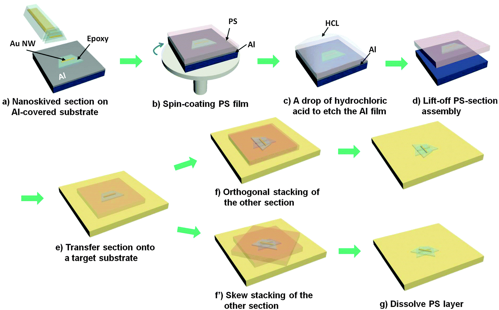 | ||
| Fig. 1 A schematic of the transfer process of sections. A layer of PS is spin-coated on a section-covered aluminum substrate. Then a drop of HCl is used to etch aluminum. So the polymer/section assembly can be lifted off and transferred onto arbitrary substrates. The stacked structures can be formed by successive transfer and control. The last step is dissolving the PS with an organic solvent. | ||
Fig. 2 shows photographic images of the transfer process. Despite the coating of the PS layer, sections are still visible to the naked eye, enabling precise control of the sections under an optical microscope (Fig. 2b). (Guides on the target substrate and/or the epoxy section can be used for further precision.) Aluminum is gradually etched as HCl penetrates the PS film, releasing the PS/epoxy-slab assembly, which can be lifted off using tweezers. (If the embedded nanostructures are acid sensitive, aluminum can be etched with NaOH instead.) The assembly can be dried by wicking the HCl solution away with a filter paper. The transfer of the assembly keeps the epoxy sections intact and uniform without wrinkles and cracks (in the epoxy slab) even after the assembly is transferred onto a target substrate, baked and the PS layer is dissolved with toluene (Fig. 2g). Sections prepared by nanoskiving can be transferred one-at-a-time or picked up from the water boat in ribbons of several sections. Both individual sections and ribbons can be transferred in a PS assembly. Since the nanostructures tend to be confined to the center of each slab, transferring ribbons allows arrays of ∼5–10 individual 2D and 3D structures to be fabricated in parallel on a target substrate.
 | ||
| Fig. 2 Photographs of a transfer procedure. (a) Sections fabricated by nanoskiving were collected on an aluminum substrate. (b) A layer of PS was spin-coated on the section-covered substrate. (c) A droplet of HCl was dropped on the surface of the PS layer. (d) The polymer–section assembly can be lifted off with the etching of aluminum. (e) The polymer–section assembly can be readily picked up using tweezers. (f) The assembly was transferred onto a silicon substrate followed by baking for 30 min at 60 °C. (g) The PS layer was dissolved by toluene. | ||
To demonstrate that the nanostructures are not damaged by the transfer or release, sections containing gold nanowires were transferred to a glass substrate. Two ends of gold nanowires were then connected with electrodes to form electrical contacts. As shown in Fig. 3, the I–V data for a typical gold nanowire are linear, indicating ohmic behavior and confirming that the gold nanowire is intact. This example also serves to highlight the gentle nature of the transfer process. Transfer methods based on sacrificial films usually employ high surface energy or strongly adhesive carrier polymers. These transfer processes work by overcoming the adhesion of the film with the substrate without detaching from the structure that is to be transferred, utilizing a difference in the adhesive force between polymer–structure and structure–substrate. The forces involved in this process could easily damage delicate (e.g., soft, organic) structures fabricated by nanoskiving which, even when embedded in an epoxy section, can be damaged by only a slight mechanical force. In addition to the gentle release and lack of reliance on adhesives, the PS layer can serve as a protective layer to enhance the stability and mechanical strength of epoxy sections.
 | ||
| Fig. 3 The linear plot of current against voltage for a gold nanowire embedded in an epoxy section that was transferred from the source substrate to a glass substrate using this process. | ||
This process can perfectly transfer sections onto arbitrary substrates, including onto pre-existing nanostructures for heterogenous integration of various nano/micro-structures into 2D or 3D structures. The flexible polymer films and the gentle operations can maintain the integrity of not only nanostructures embedded in sections, but also the original structures on substrates. Fig. 4A and B show SEM images of a gold nanowire array over nanocrescent arrays and gold nanohole arrays. Nanocrescent arrays were fabricated by the combination of soft lithography and nanoskiving and gold nanohole arrays were generated via colloidal lithography (more details can be found in the ESI†). After a PS film containing epoxy sections with embedded nanowire arrays is lightly placed on them, the gentle dissolution of PS has no deleterious effect on the existing structures. Further, by aligning nanowire arrays, gold nanogrids were constructed with intersection angles of 45° and 90°. These structures can be made by magnetic mooring as well, but perfect-transfer extends the scope of target substrates; sections can be transferred onto gold, ITO, and even non-planar surfaces, for example. And many sections can be prepared all-at-once at the ultramicrotome and stored on aluminum substrates for on-demand release and transfer. The PS–section–aluminum assemblies are sufficiently robust for shipping as well, facilitating cross-lab collaboration.
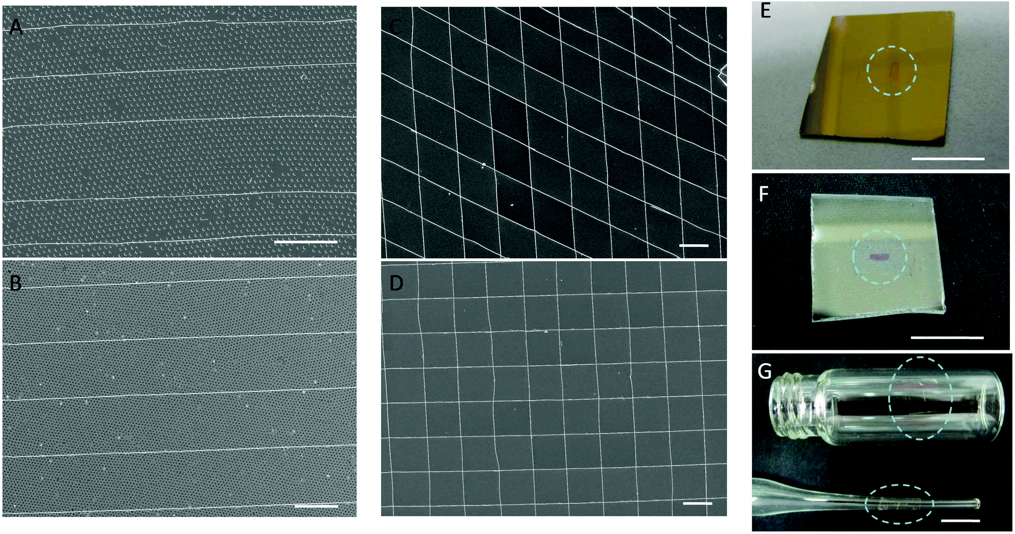 | ||
| Fig. 4 Nanostructures embedded in epoxy sections can be transferred onto arbitrary substrates, including onto existing structures. (A–D) SEM images of gold nanowire arrays over nanocrescent arrays (A) and nanohole arrays (B), and gold nanogrids with an intersection angle of 45° (C) and 90° (D). Scale bar: 10 μm. In the meantime, sections can be transferred onto gold (E), ITO (F), and non-planar surfaces (G). Scale bar: 1 cm. | ||
To demonstrate the fidelity of the transfer over macroscopic areas, we performed SERS measurements on the gold nanogrids and the nanowires over nanocrescent arrays (as shown in Fig. S2, ESI†). The intensity from the crossing point of 90° is a factor of 2.5 greater than that from a single nanowire (C–S stretch at 1077 cm−1 was used for comparison). Notably, the crossing point of 45° generates a signal, stronger by a factor of 6.7 compared to that from a single nanowire. This observation suggests that 3D-packed structures improve the electric field enhancement, which may originate from a strong and intense localized electromagnetic field (hot spots) at the crossing point.21 In the meantime, the intensity of the Raman spectra from the nanowires over nanocrescents generates a stronger signal by a factor of 1.9 compared to that from the nanocrescents.
Before release, sections can be accurately controlled and positioned onto a place, irrespective of the hydrophobicity of the target substrate and regardless of whether the epoxy matrix of the previous section is etched or not. As shown in Fig. 5, nanowires embedded in sections can easily be aligned to form 2D or stacked 3D structures by rotating successive sections containing arrays of parallel nanowires before dissolution of the PS layer and etching of the epoxy matrices. When nanowires are periodically stacked with orthogonal arrangements, they can form rectangular, ordered 3D structures (Fig. 5A). If the intersection angle is changed to 60°, the nanowires form equilateral triangles (Fig. 5B) or other geometric shapes. Individual nanowires can also be assembled parallel to each other with equal (or non-equal) spacing (Fig. 5C), which is a more flexible method for creating parallel nanowire assemblies than sectioning stacked films by nanoskiving. There is presumably no limit to how many nanostructure-containing epoxy sections can be oriented and stacked by perfect-transfer. We estimate that the positional and rotational accuracies of the features shown in Fig. 5C and Fig. S3 (ESI†) (which were transferred by hand) are 600 nm and 8°, respectively.
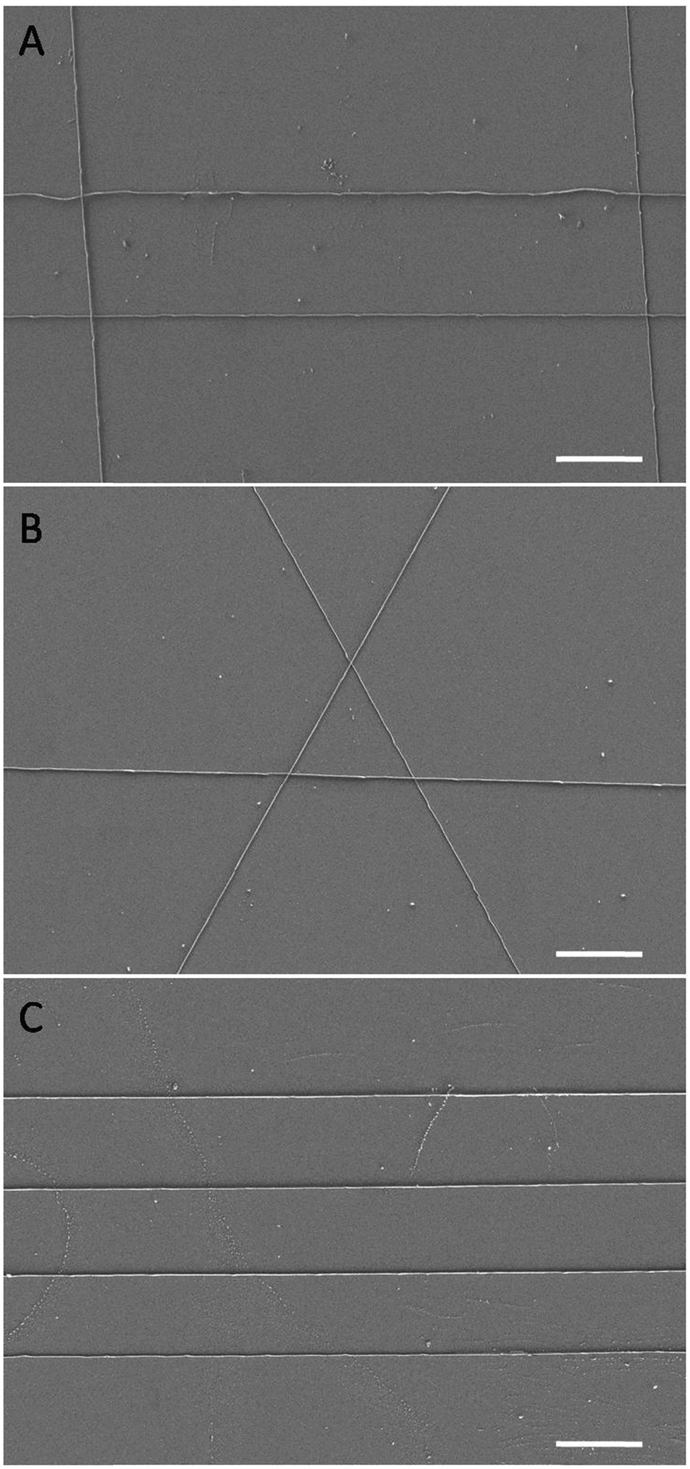 | ||
| Fig. 5 SEM images of the assemblies of gold nanowires through the process of transfer and manipulation. Gold nanowires were successively stacked to construct 2D or 3D structures, including (A) rectangular, (B) equilateral triangle, and (C) parallel structures. Scale bar: 10 μm. | ||
This process is not limited to nanostructures formed by nanoskiving; it can transfer structures formed by various methods and combinations of methods. The only restriction is that the nano/microassemblies be placed on an aluminum substrate. Subwavelength nanohole arrays patterned in a metal have extraordinary optical transmission;22 they have become one of the most extensively studied plasmonic structures for applications in spectroscopy,23,24 biosensing,25,26 and color filtering.27 They are not formed by nanoskiving, but are compatible with perfect-transfer. Large-area gold nanohole arrays were fabricated on an aluminum substrate by colloidal lithography with 380 nm diameter and 700 nm periodicity and then PS layers were spin-coated on top of them. After releasing the PS layers, the nanohole arrays could be transferred to a target substrate as described above. An SEM image of a periodic gold nanohole array, post-transfer, is shown in Fig. 6A. There is no discernable difference between the as-prepared and transferred arrays; importantly the periodicity and size are unaffected. To demonstrate this preservation, the optical transmission spectra of the nanohole arrays were measured before and after the transfer process (Fig. 6B). The nanohole array exhibits two main peaks at wavelengths of 517 nm and 1260 nm, demonstrating that the perfect transfer process can maintain the integrity of any nanostructure.
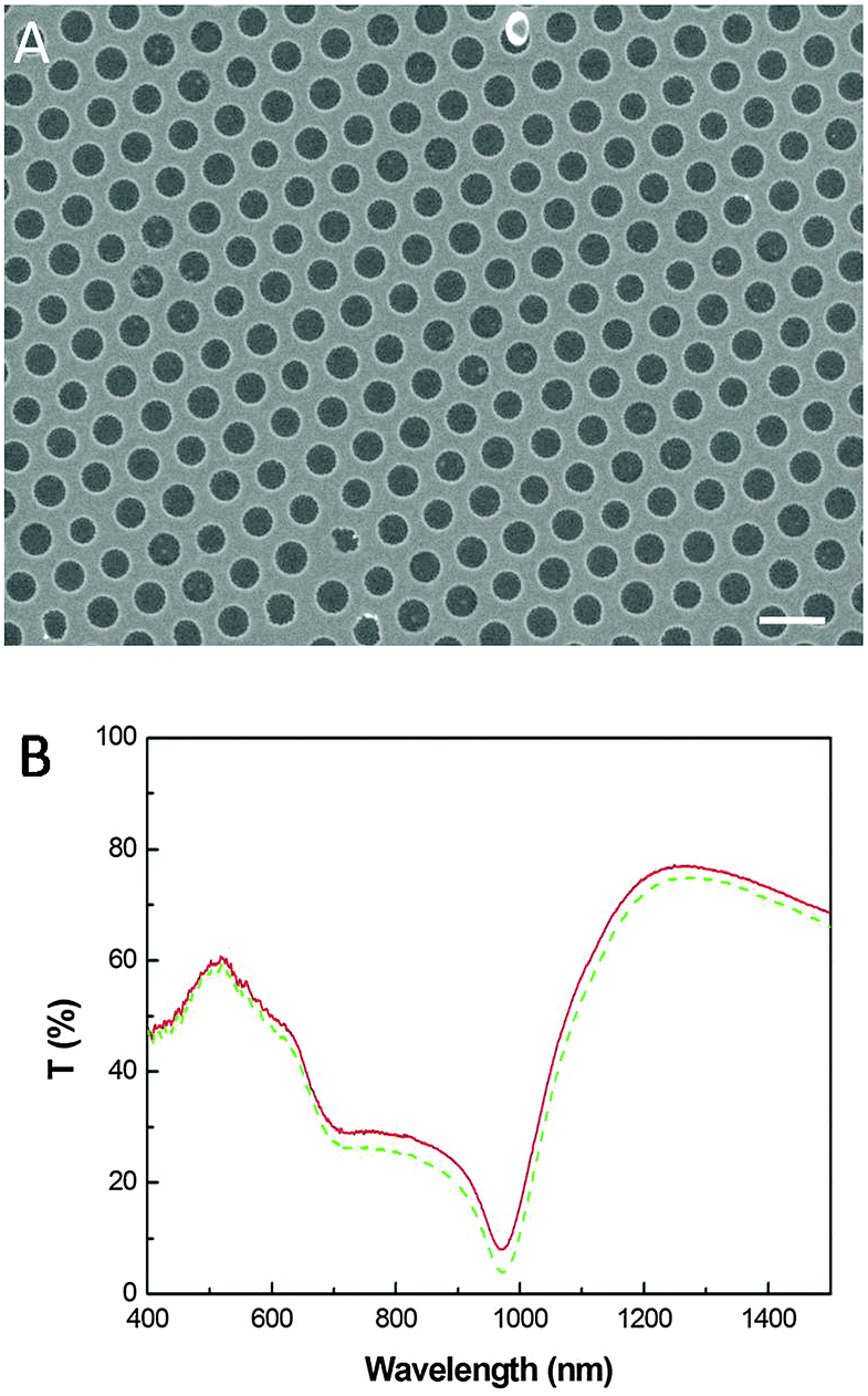 | ||
| Fig. 6 (A) SEM image of a gold nanohole array transferred from an aluminum surface to a glass substrate. Scale bar: 1 μm. (B) Transmission spectra of nanohole arrays before (red solid line) and after (green dashed line) the transfer. | ||
Conclusions
A “perfect transfer” method was demonstrated that uses a polymer film as a carrier layer and aluminum as a sacrificial layer to transfer and manipulate sections that are fabricated by nanoskiving and nanohole arrays formed via self-assembly. The yield of the transfer processes shown in this work was 100% (i.e., every transfer succeeded without error or detrimental damage.) This method affords precise control over orientation and allows structures to be stacked to produce arrays and/or 2D and 3D structures. It is simple, fast, non-damaging, does not rely on strong adhesives or high surface energies and places no constraints on the target substrate. Nanostructures transferred via this method remain intact and uniform and are free of defects, cracks, and residues (introduced by the transfer process). Many sections can be prepared at one time using an ultramicrotome and saved to be released and transferred on-demand. This method, to some extent, circumvents the dependence of nanofabrication technology on specialized, expensive equipment; stored sections can be shipped to other laboratories or used in-house, away from the ultramicrotome. No other materials (e.g., nickel for magnetic positioning) are required and the deleterious influence of capillary forces on the precise orientation of epoxy sections is eliminated. The perfect-transfer process is compatible with any nanostructures that can be placed on an aluminum substrate and should enable the fast and easy preparation of a wide variety of nanostructures that are otherwise laborious or impossible to fabricate.References
- E. J. Smythe, M. D. Dickey, G. M. Whitesides and F. Capasso, ACS Nano, 2009, 3, 59–65 CrossRef CAS PubMed.
- G. F. Schneider, V. E. Calado, H. Zandbergen, L. M. K. Vandersypen and C. Dekker, Nano Lett., 2010, 10, 1912–1916 CrossRef CAS PubMed.
- M. A. Meitl, Z.-T. Zhu, V. Kumar, K. J. Lee, X. Feng, Y. Y. Huang, I. Adesida, R. G. Nuzzo and J. A. Rogers, Nat. Mater., 2006, 5, 33–38 CrossRef CAS.
- J.-H. Ahn, H.-S. Kim, K. J. Lee, S. Jeon, S. J. Kang, Y. Sun, R. G. Nuzzo and J. A. Rogers, Science, 2006, 314, 1754–1757 CrossRef CAS PubMed.
- M. C. McAlpine, H. Ahmad, D. Wang and J. R. Heath, Nat. Mater., 2007, 6, 379–384 CrossRef CAS PubMed.
- A. Javey, S. Nam, R. S. Friedman, H. Yan and C. M. Lieber, Nano Lett., 2007, 7, 773–777 CrossRef CAS PubMed.
- X. Liang, Z. Fu and S. Y. Chou, Nano Lett., 2007, 7, 3840–3844 CrossRef CAS.
- L. B. Gao, G. X. Ni, Y. P. Liu, B. Liu, A. H. C. Neto and K. P. Loh, Nature, 2014, 505, 190–194 CrossRef CAS PubMed.
- X. Li, W. Cai, J. An, S. Kim, J. Nah, D. Yang, R. Piner, A. Velamakanni, I. Jung, E. Tutuc, S. K. Banerjee, L. Colombo and R. S. Ruoff, Science, 2009, 324, 1312–1314 CrossRef CAS PubMed.
- X. Li, Y. Zhu, W. Cai, M. Borysiak, B. Han, D. Chen, R. Piner, L. Colombo and R. S. Ruoff, Nano Lett., 2009, 9, 4359–4363 CrossRef CAS PubMed.
- S. J. Kim, T. Choi, B. Lee, S. Lee, K. Choi, J. B. Park, J. M. Yoo, Y. S. Choi, J. Ryu, P. Kim, J. Hone and B. H. Hong, Nano Lett., 2015, 15, 3236–3240 CrossRef CAS PubMed.
- K. K. Liu, W. J. Zhang, Y. H. Lee, Y. C. Lin, M. T. Chang, C. Su, C. S. Chang, H. Li, Y. M. Shi and H. Zhang, Nano Lett., 2012, 12, 1538–1544 CrossRef CAS PubMed.
- A. Gurarslan, Y. Yu, L. Su, Y. Yu, F. Suarez, S. Yao, Y. Zhu, M. Ozturk, Y. Zhang and L. Cao, ACS Nano, 2014, 8, 11522–11528 CrossRef CAS PubMed.
- Y. C. Lin, W. J. Zhang, J. K. Huang, K. K. Liu, Y. H. Lee, C. T. Liang, C. W. Chu and L. J. Li, Nanoscale, 2012, 4, 6637–6641 RSC.
- W. Cheng, M. J. Campolongo, S. J. Tanb and D. Luo, Nano Today, 2009, 4, 482–493 CrossRef CAS.
- T. Fujie, Y. Okamura and S. Takeoka, Adv. Mater., 2007, 19, 3549–3553 CrossRef CAS.
- S. Zhao, C. Hu, X. Chen, J. Zhou, Y. Jiao, K. Zhang and Y. Fu, Soft Matter, 2012, 8, 937–941 RSC.
- Q. Xu, R. M. Rioux, M. D. Dickey and G. M. Whitesides, Acc. Chem. Res., 2008, 41, 1566–1577 CrossRef CAS PubMed.
- D. J. Lipomi, R. V. Martinez and G. M. Whitesides, Angew. Chem., Int. Ed., 2011, 50, 8566–8583 CrossRef CAS PubMed.
- D. J. Lipomi, F. Ilievski, B. J. Wiley, P. B. Deotare, M. Loncar and G. M. Whitesides, ACS Nano, 2009, 3, 3315–3325 CrossRef CAS PubMed.
- Z. Zhou, Z. Zhao, Y. Yu, B. Ai, H. Möhwald, R. C. Ryan, J. K. W. Yang and G. Zhang, Adv. Mater., 2016, 28, 2956–2963 CrossRef CAS PubMed.
- T. W. Ebbesen, H. J. Lezec, H. F. Ghaemi, T. Thio and P. Wolff, Nature, 1998, 391, 667–669 CrossRef CAS.
- A. G. Brolo, E. Arctander, R. Gordon, B. Leathem and K. L. Kavanagh, Nano Lett., 2004, 4, 2015–2018 CrossRef CAS.
- J. A. Hutchison, D. M. O'Carroll, T. Schwartz, C. Genet and T. W. Ebbesen, Angew. Chem., Int. Ed., 2011, 50, 2085–2089 CrossRef CAS PubMed.
- A. G. Brolo, R. Gordon, B. Leathem and K. L. Kavanagh, Langmuir, 2004, 20, 4813–4815 CrossRef CAS PubMed.
- A. Lesuffleur, H. Im, N. C. Lindquist and S.-H. Oh, Appl. Phys. Lett., 2007, 90, 243110 CrossRef.
- T. Xu, Y.-K. Wu, X. Luo and L. J. Guo, Nat. Commun., 2010, 1, 59 Search PubMed.
Footnote |
| † Electronic supplementary information (ESI) available. See DOI: 10.1039/c6nh00099a |
| This journal is © The Royal Society of Chemistry 2016 |