
Amorphous ZnO based resistive random access memory
Yong Huangab,
Zihan Shenac,
Ye Wua,
Xiaoqiu Wangb,
Shufang Zhanga,
Xiaoqin Shia and
Haibo Zeng*a
aInstitute of Optoelectronics & Nanomaterials, School of Materials Science and Engineering, Nanjing University of Science and Technology, Nanjing 210094, China. E-mail: zeng.haibo@njust.edu.cn
bDepartment of Fundamental Courses, Jinling Institute of Technology, Nanjing 211169, China
cCollege of Elite Education, Nanjing University of Science and Technology, Nanjing 210094, China
First published on 27th January 2016
Abstract
Amorphous zinc oxide (a-ZnO) based resistive random access memory (RRAM) Ag/a-ZnO/Pt devices were fabricated and their resistive switching characteristics investigated. The Ag/a-ZnO/Pt RRAMs exhibit typical bipolar resistive switching features with the resistance ratio of high to low resistance states (HRS/LRS) more than 107. Detailed current–voltage I–V characteristic analysis suggests that the conduction mechanism in the low resistance state is due to the formation of metallic filaments. Schottky emission is proven to be the dominant conduction mechanism in the high resistance state which results from the Schottky contacts between the metal electrodes and ZnO. The Ag/a-ZnO/Pt devices also show excellent retention performance. These results suggest promising application potentials for Ag/a-ZnO/Pt RRAMs.
1. Introduction
Reversible resistive switching (RS) behavior provides a good base for resistive random access memory (RRAM) to be applied in the field of information storage. A RRAM cell usually is composed of an insulating layer sandwiched between two conductors, which load voltages to form the high (HRS) and low resistance states (LRS) corresponding to the OFF and ON of memory. Among various memories, RRAM has attracted intensive attention due to its outstanding advantages, including simple structure, fast switching, low power consumption and favorable scalability.1,2 Furthermore, RRAMs with bipolar resistive switching (BRS) behavior based on transition-metal oxides (TMO), such as Ta2O5, NiOx, HfOx, TiO2 and ZrO2, have been taken as the next generation nonvolatile memory.3–8Among these oxides, ZnO has been studied extensively in recent years for its unique properties and potential applications of electronic and optoelectronic devices,9–11 which has a wide band gap (3.37 eV at room temperature), high melting point, excellent chemical stability, is easy to control, its resistivity, etc. BRS characteristics have been observed in Al/ZnO/Si, Ag/ZnO/Pt, Cr/ZnO/Pt, Al/ZnO/Pt, Cu/ZnO/Pt, and Pt/ZnO/Pt devices,12–18 etc. However, all of the reported ZnO films for RRAM are of polycrystalline wurtzite structure according to authors' knowledge. And, there are no reports about the RS properties of amorphous zinc oxide (a-ZnO) films.
In this work, we report high-performance RRAM devices by depositing a-ZnO thin films at room temperature (RT). The Ag/a-ZnO/Pt RRAMs exhibit typical bipolar resistive switching features with the resistance ratio of high to low resistance states (HRS/LRS) more than 107, which is comparable with the highest HRS/LRS ratio of polycrystalline ZnO RRAM. The underlying switching mechanism was studied based on the transport features.
2. Experimental section
The proposed RRAM devices were deposited on commercial Pt/Ti/SiO2/Si substrates by radio frequency magnetron sputtering using a ZnO ceramic target. Growth conditions were optimized to grow amorphous layers. The sputtering was carried out in a mixed atmosphere of 50% argon (10 sccm) and 50% oxygen (10 sccm) at RT with RF power of 75 W and pressure of 1.5 Pa. For the RS property measurements, Ag top electrodes of 300 μm in diameter were deposited at RT by sputtering using a metal shadow mask to form an Ag/a-ZnO/Pt structure. Scan electron microscopy (SEM) was used to characterize the microstructure and thickness of the film. The current–voltage (I–V) characteristics of the Ag/a-ZnO/Pt structures were measured at RT in air using a Keithley 4200 semiconductor characterization system. The RS endurance characteristics were also examined by voltage sweep mode at RT. The retention characteristic was investigated up to 106 seconds at RT with reading voltage of 0.1 V. For RS speed measurement, the transient voltage was monitored using a digital oscilloscope (Lecroy 62Xi) while an electric pulse was applied by a pulse generator (Agilent 81110A).3. Results and discussion
Fig. 1(a) presents a scan electron microscopy (SEM) image of a typical cross-section of an as-fabricated ZnO/Pt/Ti/SiO2/Si structure, showing the ZnO thin film with thickness of about 100 nm. Remarkably, completely amorphous ZnO film has been achieved, which can be clearly verified by the X-ray diffraction (XRD) pattern as shown in Fig. 1(b). Besides (111) diffraction peak of Pt, we didn't find any peak from crystalline ZnO even amplifying the curve in the range of the strongest diffraction peak of ZnO. Such completely amorphous state was formed due to the applied low substrate temperature, which provides the low mobility of the sputtered species from target, and hence leads them to be “frozen” in the random positions. It has been believed that an amorphous phase of ZnO, where there are no grain boundaries, would be desirable as a channel material in high-speed electronic devices. The amorphous ZnO thin film instead of the crystallized one was employed in view of better mobility of oxygen vacancies or ions in an open matrix. So it is beneficial to stabilize resistive switching performances. | ||
| Fig. 1 (a) The cross-section SEM image of a ZnO/Pt/Ti/SiO2/Si structure without top electrodes. (b) XRD pattern of ZnO thin film deposited on Pt/Ti/SiO2/Si substrate. The inset is an enlarged image of the rectangle region without any crystalline ZnO peak. | ||
A schematic configuration of our two-terminal memory cell based on a-ZnO is shown in the inset of Fig. 2(a). The bias was applied to the Ag top electrode (TE) and the Pt bottom electrode (BE) was grounded. The reproducible I–V characteristics of the memory cell are depicted in both linear (Fig. 2(a)) and semilogarithmic (Fig. 2(b)) scales. During the measurements, the voltage bias was applied in a sweeping sequence of 1 → 2 → 3 → 4. As shown in Fig. 2(a) and (b), by steadily increasing the positive voltage from 0 to 1 V imposed on the pristine device, a sudden current increase was observed around 0.24 V, and the HRS was switched to LRS, which is called the “set” process. As the voltage from 1 V to 0 was applied, the LRS was maintained. Continuing to apply reverse voltage bias from 0 to −2 V, the device gradually switched back to HRS again starting at −0.2 V, which is called the “reset” process. Then, sweeping from −2 V to 0, the HRS was maintained. In order to protect the device from abnormally high leakage current, 0.5 mA current compliance (CC) was applied during the set process. In the subsequent I–V cycles after the first cycle, the device can switch abruptly to LRS in the voltage range from 0.15 V to 0.45 V. By increasing the negative voltage imposed on the device, the device gradually switches back to HRS again. As can be seen in Fig. 2(a) and (b), the device shows the forming-free and the bipolar resistive switching behavior with a sharp set and a gradual reset. A high forming voltage is not needed to initiate the switching for the as-fabricated devices, which may be due to the amorphous ZnO thin film instead of the crystallized one. And where there are no grain boundaries, would be desirable as a channel material in resistive switching devices. In most cases, an electroforming process is needed to activate the bipolar resistive switching. However, negative effects of electroforming process such as destruction of the electrodes will affect the stability of the device. So the forming-free property is in favor of its future application. In addition, it is calculated that the pristine cells always have a very high resistance >1010 Ω and the ROFF/RON of the device reaches 107, which is an ultrahigh memory margin, making the periphery circuit very easy to distinguish the storage information (“1” or “0”).
 | ||
| Fig. 2 (a) Typical bipolar I–V curve of the Ag/a-ZnO/Pt device is shown in linear scale and (b) semilogarithmic scale. The inset shows the schematic configuration of the Ag/a-ZnO/Pt device. (c) Enlarged OFF-state I–V curve. (d) The corresponding band diagram of ZnO sandwiched between Ag and Pt electrodes. | ||
Fig. 2(c) highlights the OFF state (or HRS) I–V curve of Fig. 2(a) and (b). The important feature is the asymmetry with respect to the bias voltage. We see that the current demonstrates a clear weak rectifying effect with a higher current value in the negative voltage branch. As for the OFF state I–V asymmetry, the structure of Ag/a-ZnO/Pt corresponds to two back-to-back asymmetric Schottky barriers (SBs) at Ag/ZnO and ZnO/Pt junctions, and the band structure is asymmetric due to different SB heights of Ag/ZnO (∼0.16 eV) and ZnO/Pt (∼1.55 eV), respectively, as schematically illustrated in Fig. 2(d).
The programming speed of the Ag/a-ZnO/Pt devices was tested by applying pulse stimuli, and a sequence of write/erase cycles stimulated by short pulses, namely, 3 V 20 ns bias for writing and −3 V 300 ns bias for erasing, respectively. The measurements were conducted after the as-prepared memory cell underwent a few switching cycles to get steady, and a small dc voltage of 0.1 V was used to read out the resistance states in the intervals of neighboring pulses. When a write pulse was applied on the device, a switching from OFF state to ON state was triggered with a large current as well as a low resistance recorded in the following read period. In contrast, an erase pulse switches the device back to OFF state. The switching process is reproducible from cycle to cycle although the write speed is far more than the erase speed, which confirms the feasibility of steep set and gradual reset as depicted in Fig. 2(b). However, this programming speed is desirable for practical memory application.
In order to further understand the switching mechanisms of such a-ZnO RRAM, the positive part of the switching curve is reploted in double logarithmic coordinates as shown in Fig. 3(a). According to the linear fitting (green lines in the figure), it is found that the I–V relationship in LRS exhibits an Ohmic conduction behavior with a slope of 1, which is regarded to the formation of conductive filaments in the device during the “set” process. At the HRS, the slope of the log(I)–log(V) line is 0.26. This result can be well explained by Schottky Emission mechanism. For such I–V characteristic of HRS, there are three candidate leakage mechanisms, namely, space-charge-limited current (SCLC),19 Poole–Frenkel (PF) emission,20 and Schottky emission.21 The corresponding I–V curves can be described following different relations, where e is the electronic charge, εr is the relative dielectric constant, ε0 is the permittivity of free space, d is the film thickness, k is Boltzmann's constant, and T is the temperature. Obviously, there are linear relationships of I vs. V2, ln(I/V) vs. V1/2, and ln![[thin space (1/6-em)]](https://www.rsc.org/images/entities/char_2009.gif) I vs. V1/2 for SCLC, PF, and Schottky mechanism, respectively.
I vs. V1/2 for SCLC, PF, and Schottky mechanism, respectively.
| (SCLC) I ∝ εrε0μV2, | (1) |
 | (2) |
 | (3) |
 | ||
| Fig. 3 (a) The positive part of the switching curve is re-plotted in a double-logarithmic coordinate. (b)–(d) The plots of I–V2, ln(I/V)–V1/2 and lnI–V1/2 for the SCLC, PF and Schottky conduction mechanisms, respectively. The straight line is linear fitting. | ||
The I–V curves of HRS were re-plotted in these three kinds of scales as shown in Fig. 3(b)–(d). Very obviously, among these three re-plotted curves, the linearity degree of the lnI vs. V1/2 curve is the highest, which demonstrates that the conduction mechanism of HRS is dominated by Schottky Emission mechanism.
Up to now, the filamentary switching mechanisms in RRAM are still subjects of heated debate and controversy. In previous work,18 an oxygen-vacancy filament growth mode has been proposed for Ag/ZnO/Pt RRAM cells. Here, we proposed a different but reasonable explanation related to the filament formation and rupture, because the RS effect in our case is very likely to be mediated by electrochemical metallization (ECM).2,13 Fig. 4(a) shows the pristine state of the Ag/a-ZnO/Pt memory cell. It is generally recognized that the Ag electrode is an active component in filament formation for ECM cells while Pt electrode is inert. When a positive voltage is applied to Ag TE, oxidation occurs on this electrochemically active material. Therefore Ag+ cations are generated, which could be described as Ag → Ag+ + e−. The mobile Ag+ cations migrate toward Pt BE through the a-ZnO layer and are reduced there by electrons flowing from the cathode, i.e., Ag+ + e− → Ag (Fig. 4(b)–(d)). The successive precipitations of Ag metal atoms at the cathode lead to a growth of the Ag protrusion, which finally reaches the TE and forms a highly conductive filament in the ON state (Fig. 4(d)). When the polarity of the applied voltage is reversed, an electrochemical dissolution takes place somewhere along the filament and which is almost completely dissolved, resetting the system into the OFF state (Fig. 4(e)). Thus, the following SET process needs to rejuvenate the previously ruptured filament segment by almost the same SET voltage compared to the previous SET process (Fig. 4(f)).
 | ||
| Fig. 4 A schematic diagram for the mechanism of resistive switching effects in Ag/a-ZnO/Pt devices. (a) Pristine state. (b)–(c) The oxidation of Ag at TE and the migration of the mobile Ag+ cations toward the cathode and their reductions therein. (d) The precipitations of Ag metal atoms at the Pt electrode lead to a growth of Ag filament and finally form a highly conductive filament in the cell. (e) When the polarity of the applied voltage is reversed, an electrochemical dissolution of the filament takes place, resetting the cell into the OFF state. (f) The next SET process. | ||
Fig. 5(a) and (b) show the temperature dependence of RON and ROFF of the device, respectively. As shown in Fig. 5(a), RON exhibits a decreasing trend when the ambient temperature decreases. This is a typical electronic transport behavior for a metal, in which phonon scattering is dominant. The temperature dependence of metallic resistance can be written as R(T) = R0[1 + α(T − T0)], where R0 is the resistance at temperature T0, and α is the temperature coefficient of resistance. Our fitting results for RON–T comply with this linear dependence (Fig. 5(a)); therefore the filaments are composed of Ag. This judgment is also supported by the linear I–V characteristics of LRS as shown in Fig. 2(a) and Fig. 3(a). By choosing T0 as 300 K, the R of the filaments is further calculated to be 4.5 × 10⁻³ K−1, which is consistent with the literature reported by Bid et al.22 On the other hand, Fig. 5(b) shows that ROFF decreases with increasing temperature, and it exhibits an approximate relationship logROFF ∝ T, which could be ascribed to a typical semiconducting behavior. The temperature dependence of current in a semiconductor follows
| I = I0exp(−ϕtκT) |
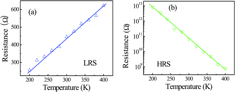 | ||
| Fig. 5 (a) Temperature dependence of RON of the device. RON decreases linearly with decreasing the ambient temperature, indicating that the filaments are in metallic states. (b) Temperature dependence of ROFF of the device, implying a semiconducting character. | ||
To investigate the RS performances of the Ag/a-ZnO/Pt memory, cycle-to-cycle switching voltage and resistance states were analyzed statistically. Fig. 6(a) shows the distributions of the switching threshold voltages (VSET and VRESET) of the device. The VSET have narrower distributions than VRESET during 100 I–V cycles, demonstrating a very stable set process. Fig. 6(b) shows the evolution of HRS and LRS in 100 I–V cycles under a small reading voltage of 0.1 V. As can be seen, the variation of HRS and LRS during cycling is very little and the memory window always keeps beyond 107 without degradation. The above endurance measurements ensured that the RS properties in Ag/a-ZnO/Pt devices are highly reliable and reproducible. The retention performance of the memory cell at RT is illustrated in Fig. 6(c). ROFF/RON over 107 remains nearly constant during the retention time of 106 s, confirming the nonvolatile characteristics of our device. The device-to-device distribution of resistance switching parameters have also been investigated. When test was performed on 40 devices, slightly wider range of switching voltage and resistance distribution was found in Fig. 6(d) and (e). The distribution is not much wider making the device suitable for memory applications. Additionally, we estimated the cell yield. Despite some cells fail to show RS, all of 40 devices were observed to exhibit similar RS, indicating that the overall device yield is 100%.
 | ||
| Fig. 6 (a) The distributions of the threshold voltages of the Ag/a-ZnO/Pt memory cell. (b) Endurance performances up to 100 switching cycles. The HRS and LRS resistance values were read out at 0.1 V in each sweep. (c) Retention performance, indicating stable HRS and LRS for up to 106 s at RT. The device-to-device distribution of switching voltage (d) and resistance (e). | ||
Interestingly, almost a year later, the devices were retested and the multilevel resistance states were achieved under different compliance current (CC) during set processes, as depicted in Fig. 7(a). Obviously, the CC plays a significant role in RS characteristic, especially in the resistance of LRS and the current of reset process. The resistance of LRS could be controlled by changing the CC during the set process. Under different CC values of 0.1 mA, 0.2 mA, 0.3 mA, 0.4 mA and 0.5 mA, five switching states with different resistance values can be clearly distinguished. As can be seen from Fig. 7(b), the higher the CC imposed on the cell, the lower the resistance value in LRS (2402 Ω, 1260 Ω, 1017 Ω, 772 Ω, 568 Ω, respectively). Moreover, the resistance of the HRS (37 MΩ, 176 MΩ, 24 MΩ, 28 MΩ, 97 MΩ, respectively) was basically in the same magnitude under various applied CC. And the ON/OFF ratio still kept 104 to 105 even after one year. Additionally, reversible and stable RS behavior can't be observed while CC > 0.5 mA or CC < 0.1 mA. The resistance of the HRS was not influenced much by CC, while that of LRS was decreased obviously with increase of CC. This is because the bigger CC was applied, the stronger conductive filaments were formed in the ZnO layer during SET process. Furthermore, the bigger CC brought about the longer RESET time. The RESET time varied from 120 ns to 300 ns depending on different CC. When 0.1 mA CC was applied, the RESET time was as short as 120 ns, but such a short RESET process was not too stable compared to 0.5 mA CC and 300 ns RESET time. From these results, therefore, it is important to examine the device performance by appropriate CC and switching speed.
 | ||
| Fig. 7 (a) The multilevel switching characteristics of the device under different compliance currents (0.1, 0.2, 0.3, 0.4, and 0.5 mA). (b) The resistance of the HRS and the LRS under different CC. | ||
All these data demonstrated that stable RS performances of the Ag/a-ZnO/Pt memory can be realized by this simple method and meet the requirement for RRAM device application.
4. Conclusions
In conclusion, we have demonstrated that 100 nm-thick amorphous ZnO thin films prepared by radio frequency magnetron sputtering at room temperature exhibit excellent nonvolatile bipolar resistive switching behavior with a large ROFF/RON ratio (>107, kept 104 to 105 even after one year), stable endurance, and long retention. The observed resistive switching performance of the amorphous ZnO is as good as polycrystalline one, which could be attributed to the formation/rupture of Ag nanofilaments in amorphous ZnO thin films based on the electrochemical metallization mechanism. The simple structure and fully room-temperature-fabricated procedure of the device make it very attractive for future applications of nonvolatile resistive switching memory.Acknowledgements
We would like to thank Prof. Fei Zhuge for his kind help in our preparation of this paper. This work was supported by the National 973 project from National Basic Research Program of China (2014CB931700 and 2014CB931702), the National Natural Science Foundation of China (61222403, 21403112 and 51402152), China Postdoctoral Science Foundation (2014M551595), the Natural Science Foundation of Jiangsu Province (BK20140778), and the Scientific Foundation of Jinling Institute of Technology (jit-rcyj-201403 and jit-n-201533).References
- A. Sawa, Mater. Today, 2008, 11, 28–36 CrossRef CAS
.
- R. Waser, R. Dittmann, G. Staikov and K. Szot, Adv. Mater., 2009, 21, 2632–2663 CrossRef CAS
- Y. L. Chung, W. H. Cheng, J. S. Jeng, W. C. Chen, S. A. Jhan and J. S. Chen, J. Appl. Phys., 2014, 116 Search PubMed
- D. Panda, A. Dhar and S. K. Ray, IEEE Trans. Nanotechnol., 2012, 11, 51–55 CrossRef
- J. Shang, G. Liu, H. L. Yang, X. J. Zhu, X. X. Chen, H. W. Tan, B. L. Hu, L. Pan, W. H. Xue and R. W. Li, Adv. Funct. Mater., 2014, 24, 2171–2179 CrossRef CAS
- J. Sun, Q. Liu, H. W. Xie, X. Wu, F. Xu, T. Xu, S. B. Long, H. B. Lv, Y. T. Li, L. T. Sun and M. Liu, Appl. Phys. Lett., 2013, 102 Search PubMed
- H. J. Kim, Y.-J. Baek, Y. J. Choi, C. J. Kang, H. H. Lee, H.-M. Kim, K.-B. Kim and T.-S. Yoon, RSC Adv., 2013, 3, 20978 RSC
- D.-H. Lim, G.-Y. Kim, J.-H. Song, K.-S. Jeong, D.-C. Kim, S.-W. Nam, M.-H. Cho and T.-G. Lee, RSC Adv., 2015, 5, 221–230 RSC
- Y. Huang, Y. Luo, Z. H. Shen, G. L. Yuan and H. B. Zeng, Nanoscale Res. Lett., 2014, 9 CAS
- H. B. Zeng, G. T. Duan, Y. Li, S. K. Yang, X. X. Xu and W. P. Cai, Adv. Funct. Mater., 2010, 20, 561–572 CrossRef CAS
- J. L. Campbell, M. Breedon, K. Latham and K. Kalantar-Zadeh, Langmuir, 2008, 24, 5091–5098 CrossRef CAS PubMed
- C. Chen, F. Pan, Z. S. Wang, J. Yang and F. Zeng, J. Appl. Phys., 2012, 111 CrossRef
- Y. C. Yang, F. Pan, Q. Liu, M. Liu and F. Zeng, Nano Lett., 2009, 9, 1636–1643 CrossRef CAS PubMed
- W. Y. Chang, H. W. Huang, W. T. Wang, C. H. Hou, Y. L. Chueh and J. H. He, J. Electrochem. Soc., 2012, 159, G29–G32 CrossRef CAS
- S. S. Peng, F. Zhuge, X. X. Chen, X. J. Zhu, B. L. Hu, L. Pan, B. Chen and R. W. Li, Appl. Phys. Lett., 2012, 100 Search PubMed
- J. J. Ke, Z. J. Liu, C. F. Kang, S. J. Lin and J. H. He, Appl. Phys. Lett., 2011, 99 Search PubMed
- J. Zhang, H. Yang, Q. L. Zhang, S. R. Dong and J. K. Luo, Appl. Phys. Lett., 2013, 102 Search PubMed
- A. S. Zoolfakar, R. Ab Kadir, R. A. Rani, S. Balendhran, X. J. Liu, E. Kats, S. K. Bhargava, M. Bhaskaran, S. Sriram, S. Zhuiykov, A. P. O'Mullane and K. Kalantar-zadeh, Phys. Chem. Chem. Phys., 2013, 15, 10376–10384 RSC
- M. A. Lampert, Phys. Rev., 1956, 103, 1648–1656 CrossRef CAS
- J. R. Yeargan, J. Appl. Phys., 1968, 39, 5600 CrossRef CAS
- P. R. Emtage and W. Tantraporn, Phys. Rev. Lett., 1962, 8, 267–268 CrossRef
- A. Bid, A. Bora and A. K. Raychaudhuri, Phys. Rev. B: Condens. Matter Mater. Phys., 2006, 74 Search PubMed
| This journal is © The Royal Society of Chemistry 2016 |