Fabrication of a resist pattern based on plasma–polystyrene interactions†
Ning Li,
Lei Feng,
Fei Teng,
Yandong Wang,
Feifei Wu,
Xiangchao Yang and
Nan Lu*
State Key Laboratory of Supramolecular Structure and Materials, College of Chemistry, Jilin University, Changchun 130012, P.R. China. E-mail: luenan@jlu.edu.cn
First published on 29th January 2016
Abstract
We report a straightforward method to fabricate resist patterns based on the interaction of oxygen plasma and polystyrene (PS) spheres within several minutes. The XPS results demonstrate that the resist pattern is formed by the PS fragments produced in the etching process. In the process, PS spheres not only serve as templates for patterning, but also provide PS fragments to form the resist pattern. The ultrathin resist (UR) pattern can serve as a mask for dry etching with the selectivity of 21![[thin space (1/6-em)]](https://www.rsc.org/images/entities/char_2009.gif) :
:![[thin space (1/6-em)]](https://www.rsc.org/images/entities/char_2009.gif) 1. In addition, the resist pattern can be used as a template to selectively deposit silver nanoparticles because it can effectively block electrons.
1. In addition, the resist pattern can be used as a template to selectively deposit silver nanoparticles because it can effectively block electrons.
Motivated by the demand for denser component integration in the semiconductor industry, manufacturers and researchers have made considerable progress in high-resolution lithography techniques, such as photolithography,1 extreme ultraviolet lithography,2 electron beam lithography (EBL),3 nanoimprint lithography (NIL),4 nanosphere lithography (NSL),5 etc. For all the techniques, to transfer a pattern from the resist layer to the underlying substrate is one of the most important steps for the fabrication, which is usually completed by site-selective dry etching. In general, an ideal resist material is of high selectivity, high adhesion and sufficient mechanical stiffness.
The most conventional material is the carbon-based materials, such as polymethyl methacrylate,4 PS,6 SU-8,7 etc., but some of them have lower selectivity and poorer adhesion, moreover, they may collapse during wet development due to poor stiffness.8 In order to achieve a higher aspect ratio, some hard masks were proposed, such as hydrogen silsesquioxane (HSQ),9 sputtered metal10 and atomic layer deposition (ALD).8,11 HSQ is of relative high mechanical stability, which has been widely used in EBL,12 NIL,13 etc., however, its sensitivity to electron beam exposure is relative low,14 and its hardness depends on the bake temperature and bake time.9 Although metal film, like Au, Ag, Ni, and Cr, can be used as resist, multi-step process involved in resist patterning could limit its applications. The resist based on ALD is an ideal resist because it is highly stable and the thickness can be controlled in nanoscale, however, the fabrication process is complicated and time-consuming. For example, the substrate usually needs to be patterned and modified with hydroxyl groups in advance, and then the reaction of precursors and deposition are alternatively conducted, finally the resist are formed layer-by-layer.15 So ALD deposition rate is very slow; moreover, the deposition process is complex and costly. Therefore, to develop a simple method for creating ideal resist patterns is highly needed.
Herein, inspired by the ALD process, we developed a straightforward and efficient method to create resist pattern on silicon (Si) within several minutes by using PS spheres as source of precursor.
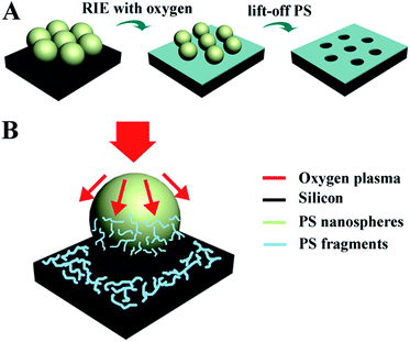
The fabrication procedure is shown in Fig. 1A. First, the monolayer of PS spheres was self-assembled on the Si slide. Then the assembled PS spheres were subjected to reactive ion etching (RIE) with oxygen. Here, the PS spheres not only served as the template for resist patterning, but also as the source of resist. The formation process of the resist pattern can be understood as Fig. 1B. The plasma flow contains ions, electrons, excited neutrals, radicals, and UV radiation. These highly reactive components lead to the chain scission of the PS molecules, generating the low-molecular-weight fragments. When the fragments with reactive radicals arrived on Si, they formed the PS fragments layer. After lifting-off the spheres in toluene, the resist pattern was obtained.
 | ||
| Fig. 1 (A) Procedure for the fabrication of resist pattern. (B) Schematic illustration of the formation for the resist pattern. | ||
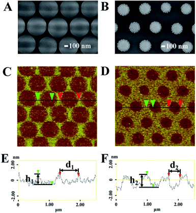
We followed the transformation of PS spheres with scanning electron microscope (SEM). The 600 nm PS spheres were assembled into hexagonally packed arrangement (detailed in Fig. S1 of the ESI†). As revealed in Fig. 2A and B, the average diameter of PS spheres was accordingly decreased to 555 and 336 nm by conducting oxygen plasma etching for 3 and 9 min, respectively. Clearly, the surface of spheres became rougher as extending the etching duration, which was introduced by the inhomogeneous etching and the detachment of the PS fragments.
After removing the PS spheres in toluene, the remained resist patterns were characterized with atomic force microscope (AFM). The topography images of the resist patterns created with different etching duration are shown in Fig. 2C and D. The section analysis (Fig. 2E and F) indicates that the average diameters of the holes on Si slides generated by 3 and 9 min etching are 593 nm (d1) and 362 nm (d2), respectively, which are slightly larger than that of the spheres. We attribute this to the anisotropic deposition caused by the horizontal movement of the plasma flow. This result shows that the features of the resist pattern can be controlled by tuning the size of spheres because they are template for the fragments deposition. As shown in Fig. 2E and F, the average thickness of the resist layer increases from 1.4 nm (h1) to 1.7 nm (h2) when the etching duration is extended from 3 to 9 min. The thickness of UR is just increased for 0.3 nm from 3 min to 9 min. During the formation of the UR, the deposition of PS fragments on Si and the reduction of the UR take place at the same time during the etching process. The thickness of the UR decreases at a constant speed, but the increase speed of the thickness for the deposited PS fragments changes with the reduction of the PS spheres because of the following reasons. Firstly, the amount of produced PS fragments decreases with the reduction of the PS spheres. Secondly, at the very beginning of the etching process, the PS fragments from the neighboring PS spheres deposit on the same place, but the overlap of the deposition will disappear when the PS spheres are small enough (detailed in Fig. S2A of the ESI†). Therefore, the maximum thickness must exist during the etching process. According to our experimental results, the maximum thickness of the UR is observed when the etching duration is 9 min under this condition. But it is difficult to determine if it is the real maximum thickness of the UR, as indicated in Fig. S2B,† it may exist when the etching time is in the range of 6 to 11 min.
To investigate the composition of the UR, we conducted XPS measurements. The carbon element of the following samples was characterized: Si after being etched for 3 min with oxygen plasma as the sample 1, i.e. the reference. Si assembled with PS after being etched for 3 min with oxygen plasma, and then PS was removed as the sample 2.
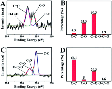
Fig. 3A and C present the fitting peaks for carbon functional groups of sample 1 and sample 2. The calculated percentage of the different carbon functional groups are accordingly shown in Fig. 3B and D. By fitting the C1s of reference, Fig. 3A identifies there are C–C (285.5 eV), C–O (286.1 eV), C![[double bond, length as m-dash]](https://www.rsc.org/images/entities/char_e001.gif) O (287.6 eV) and O–C
O (287.6 eV) and O–C![[double bond, length as m-dash]](https://www.rsc.org/images/entities/char_e001.gif) O (289.8 eV) groups. The percentage of C–C is 4.5%, C–O is 33.3%, C
O (289.8 eV) groups. The percentage of C–C is 4.5%, C–O is 33.3%, C![[double bond, length as m-dash]](https://www.rsc.org/images/entities/char_e001.gif) O is 60.3%, and O–C
O is 60.3%, and O–C![[double bond, length as m-dash]](https://www.rsc.org/images/entities/char_e001.gif) O is 1.9% (Fig. 3B). Comparing sample 2 with sample 1, they have the same kinds of functional groups (Fig. 3C), but the percentage of C–C increases from 4.5% to 64.1%, while C
O is 1.9% (Fig. 3B). Comparing sample 2 with sample 1, they have the same kinds of functional groups (Fig. 3C), but the percentage of C–C increases from 4.5% to 64.1%, while C![[double bond, length as m-dash]](https://www.rsc.org/images/entities/char_e001.gif) O drops from 33.3% to 5% (Fig. 3D). The percentage variation of C–C between sample 1 and sample 2 could be caused by the formation of UR. In order to further identify the source of the resist layer, we calculated the carbon content of sample 1 and sample 2, the ratio of sample 2
O drops from 33.3% to 5% (Fig. 3D). The percentage variation of C–C between sample 1 and sample 2 could be caused by the formation of UR. In order to further identify the source of the resist layer, we calculated the carbon content of sample 1 and sample 2, the ratio of sample 2![[thin space (1/6-em)]](https://www.rsc.org/images/entities/char_2009.gif) :
:![[thin space (1/6-em)]](https://www.rsc.org/images/entities/char_2009.gif) sample 1 is 2.27
sample 1 is 2.27![[thin space (1/6-em)]](https://www.rsc.org/images/entities/char_2009.gif) :
:![[thin space (1/6-em)]](https://www.rsc.org/images/entities/char_2009.gif) 1. It means that the carbon content on Si with PS spheres is higher than that of bare Si after treating with oxygen plasma, which confirms that the redundant carbon on Si comes from PS spheres.
1. It means that the carbon content on Si with PS spheres is higher than that of bare Si after treating with oxygen plasma, which confirms that the redundant carbon on Si comes from PS spheres.
 | ||
| Fig. 3 XPS spectra of C1s region: the spectra (left column) and percentage of different functional groups (right column) for sample 1 (A and B), and sample 2 (C and D), respectively. | ||
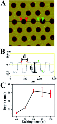
In order to test resist property of the UR for RIE, the sample (shown in Fig. 2D) was subjected to RIE for different time with SF6 gas. Fig. 4A shows that a nanohole array was created when the sample was etched for 60 s. The average depth of the nanohole is ∼24 nm (h), and the average diameter of the nanohole is ∼369 nm (d) (Fig. 4B), which is almost same as the diameter of UR pattern (Fig. 2D). The results demonstrate the etching selectivity of Si to UR is higher. The correlation of the depth of nanohole and the etching duration is presented in Fig. 4C. It presents that the depth increases with extending the duration from 60 to 80 s. When extending the RIE duration to 80 s, the depth of the nanohole was increased to ∼36 nm, and the diameter of the nanohole is ∼363 nm, which also remained the same as that of the UR pattern. However, the surface became rougher, which indicates that the UR was slightly damaged by etching process. When the etching duration was further extended to 100 s, the depth nearly remained constant, but the diameter of the nanohole was ∼398 nm, which was increased for ∼9.6% (detailed in Fig. S3 of the ESI†). This should be caused by the isotropic chemical etching of SF6. At the time, the UR has been destroyed absolutely, and the etching selectivity for Si to UR is 21![[thin space (1/6-em)]](https://www.rsc.org/images/entities/char_2009.gif) :
:![[thin space (1/6-em)]](https://www.rsc.org/images/entities/char_2009.gif) 1.
1.
To find out the difference of the spheres and the UR, we characterized the PS spheres and the UR with XPS. The peaks of C–C and C–O can be observed in both the spectra of the PS spheres (detailed in Fig. S4 of the ESI†) and the UR (Fig. 3C), the two peaks should respectively come from aliphatic and aromatic bond carbon, and the surface contamination. The peak of π → π* should come from excitations in the benzene ring,16 and it is too weak to be split from the spectra because of the lower content of benzene in the UR (Fig. 3C). But the peaks of C![[double bond, length as m-dash]](https://www.rsc.org/images/entities/char_e001.gif) O and O–C
O and O–C![[double bond, length as m-dash]](https://www.rsc.org/images/entities/char_e001.gif) O only can be found in Fig. 3C, which means that the UR is highly cross-linked. Therefore, the UR is much more dense and stable than PS spheres.
O only can be found in Fig. 3C, which means that the UR is highly cross-linked. Therefore, the UR is much more dense and stable than PS spheres.
Furthermore, in order to study the blocking property of the UR to electrons, the sample (shown in Fig. 2D) was immersed into the mixed solution of silver nitrate, hydrogen peroxide, and hydrofluoric acid, site-selective electroless silver deposition will be produced (detailed in Fig. S5 of the ESI†). The result demonstrates the resist pattern can be applied as a site-selective template, and it is stable in the reaction solution.
Conclusions
In conclusion, we present a straightforward method to fabricate resist pattern based on the interaction of oxygen plasma and PS spheres within several minutes. In the fabrication process, PS spheres not only serve as template for resist patterning, but also provide PS fragments for the formation of the UR. The UR exhibits high etching selectivity to Si, meanwhile, it is a good template for site-selective redox reactions. This method could be applied for other polymers and substrates.Acknowledgements
This work was supported by the National Natural Science Foundation of China (No. 21273092).Notes and references
- F. F. Wu, G. Shi, H. B. Xu, L. X. Liu, Y. D. Wang, D. P. Qi and N. Lu, ACS Appl. Mater. Interfaces, 2013, 5, 12799–12803 CAS.
- P. D. Ashby, D. L. Olynick, D. F. Ogletree and P. P. Naulleau, Adv. Mater., 2015, 27, 5813–5819 CrossRef CAS PubMed.
- Y. F. Chen, Microelectron. Eng., 2015, 135, 57–72 CrossRef CAS.
- F. F. Wu, L. X. Liu, L. Feng, D. R. Xu and N. Lu, Nanoscale, 2015, 7, 13026–13032 RSC.
- H. B. Xu, N. Lu, D. P. Qi, J. Y. Hao, L. G. Gao, B. Zhang and L. F. Chi, Small, 2008, 4, 1972–1975 CrossRef CAS PubMed.
- C. Con, R. Dey, M. Ferguson, J. Zhang, R. Mansour, M. Yavuz and B. Cui, Microelectron. Eng., 2012, 98, 254–257 CrossRef CAS.
- K. H. Rasmussen, S. S. Keller, F. Jensen, A. M. Jorgensen and O. Hansen, Microelectron. Eng., 2013, 112, 35–40 CrossRef CAS.
- Y. C. Tseng, A. U. Mane, J. W. Elam and S. B. Darling, Adv. Mater., 2012, 24, 2608–2613 CrossRef CAS PubMed.
- L. O'Faolain, M. V. Kotlyar, N. Tripathi, R. Wilson and T. F. Krauss, J. Vac. Sci. Technol., B: Microelectron. Nanometer Struct.--Process., Meas., Phenom., 2006, 24, 336–339 CrossRef.
- K. M. Lim, S. Gupta, C. Ropp and E. Waks, Microelectron. Eng., 2011, 88, 994–998 CrossRef CAS.
- Y. C. Tseng, Q. Peng, L. E. Ocola, D. A. Czaplewski, J. W. Elam and S. B. Darling, J. Mater. Chem., 2011, 21, 11722–11725 RSC.
- I. B. Baek, J. H. Yang, W. J. Cho, C. G. Ahn, K. Im and S. Lee, J. Vac. Sci. Technol., B: Microelectron. Nanometer Struct.--Process., Meas., Phenom., 2005, 23, 3120–3123 CrossRef CAS.
- Y. Igaku, S. Matsui, H. Ishigaki, J. Fujita, M. Ishida, Y. Ochiai, H. Namatsu, M. Komuro and H. Hiroshima, Jpn. J. Appl. Phys., Part 1, 2002, 41, 4198–4202 CrossRef CAS.
- G. M. Schmid, L. E. Carpenter and J. A. Liddle, J. Vac. Sci. Technol., B: Microelectron. Nanometer Struct.--Process., Meas., Phenom., 2004, 22, 3497–3502 CrossRef CAS.
- A. J. M. Mackus, A. A. Bol and W. M. M. Kessels, Nanoscale, 2014, 6, 10941–10960 RSC.
- L. Wegewitz, A. Prowald, J. Meuthen, S. Dahle, O. Hofft, F. Endres and W. Maus-Friedrichs, Phys. Chem. Chem. Phys., 2014, 16, 18261–18267 RSC.
Footnote |
| † Electronic supplementary information (ESI) available: Experimental details, SEM, and AFM data. See DOI: 10.1039/c5ra24879e |
| This journal is © The Royal Society of Chemistry 2016 |


