
In situ fabrication of highly crystalline CdS decorated Bi2S3 nanowires (nano-heterostructure) for visible light photocatalyst application†
Rajendra P. Panmand*a,
Yogesh A. Sethia,
Rajashree S. Deokarb,
Datta J. Latec,
Haribhau M. Gholapb,
Jin-Ook Baegd and
Bharat B. Kale*a
aCentre for Materials for Electronics Technology (C-MET), Panchawati, Off Pashanroad, Pune-411008, India. E-mail: rajendra@cmet.gov.in; bbkale@cmet.gov.in
bDepartment of Physics, Fergusson College, Pune – 411004, India
cPhysical and Materials Chemistry Division, CSIR-National Chemical Laboratory, Pashan Road, Pune 411008, India
dKorea Research Institute of Chemical Technology, Division of Green Chemistry and Engineering Research, 100 Jangdong, Yusong, Daejon, KR 305-600, South Korea
First published on 22nd February 2016
Abstract
In situ synthesis of the orthorhombic Bi2S3 nanowires decorated with hexagonal CdS nanoparticles (nano-heterostructure) has been demonstrated by a facile solvothermal method. The tiny 5–7 nm CdS spherical nanoparticles are decorated on the surfaces of 30–40 nm Bi2S3 nanowires, successfully. Structural, morphological and optical studies clearly show the existence of CdS on the nanowires. A possible sequential deposition growth mechanism is proposed on the basis of experimental results to reveal the formation of the nano heterostructure. The heterostructures have been used as a photocatalyst for hydrogen production as well as degradation of methylene blue under solar light. The maximum hydrogen evolution i.e. 4560 and 2340 μmol h−1 0.5 g was obtained from H2S splitting and glycerol degradation for Bi2S3 NWs decorated with CdS nanoparticles (nano-heterostructure) which is higher than that of the Bi2S3 NWs (3000 and 1170 μmol h−1 0.5 g, respectively). The enhanced photocatalytical hydrogen evolution efficiency of the heterostructures is mainly attributed to its nanostructure. In the nano heterostructure, the CdS nanoparticles control the charge carrier transition, recombination, and separation, while the Bi2S3 nanowire serves as a support for the CdS nanoparticles. The photogenerated electron's migration is faster than the holes from the inside of a CdS nanoparticle to its surface or to the phase interface, resulting in a relatively higher hole density inside the CdS nanoparticle leaving electron density at surface of the Bi2S3 NWs. This influences the photocatalytic activity under solar light. Such nano-heterostructures may have potential in other photocatalytic reactions.
1. Introduction
One-dimensional (1D) oxide and sulphides nanostructures, such as nanorods, nanotubes, nanowires and nanobelts, have attracted intensive interest due to their unique optical, electronic and mechanical properties, and potential application in the fabrication of photocatalysts, nanoscale electronics and optoelectronics devices.1–3 One dimensional (1D) semiconductors are considered as the most encouraging photosensitive materials due to the large surface-to-volume ratio and a Debye length comparable to their small size.4,5 The number of surface trap states and prolong photo-carrier lifetime with increase of surface-to-volume ratio, ultimately enhance the photocatalytic performance of material.6,7The photocatalytic hydrogen generation as a clean energy via abundant water, hydrogen sulphide splitting and biomass degradation using semiconductor photocatalyst has attracted much attention due to the global energy crisis and environmental problems. Till date, most of the semiconductor photocatalysts have low efficiency and instability for hydrogen evolution under the solar light. In view of this, different semiconductor heterostructures8–11 have been investigated and designed to enhance the photo-induced charge carrier's separation unlike to single phase photocatalysts.12,13
Considering the importance of the one dimensional as well as heterostructured materials for photocatalysis, many efficient and stable heterostructures for photocatalytic hydrogen generation are investigated based on different electron transfer mechanisms.14–18 For example, CdS/CeOx heterostructures show superior hydrogen generation than single CdS or CeOx due to the efficient light harvesting and fast separation of photogenerated carriers compared to CdS or CeOx. Jum Suk Jang19 and group have also reported that the molar concentration of TiO2 in CdS NW/TiO2 nanocomposite photocatalyst exhibit highest activity for H2 evolution. This configuration of photocatalyst results in an efficient charge separation due to fast diffusion of photoelectrons generated from CdS NWs toward surrounding TiO2 NP, leading to high photocatalytic activity of hydrogen production. The CdS accompanied with host material such as ZnO and CdLnS4, alter the energy levels of the conduction and valence bands in the coupled semiconductor system which helps to enhanced hydrogen generation via water splitting.20,21 Recently, Zhen Fang et al. demonstrated that a growth of CdS on Bi2S3 nanostructures may exhibit high hydrogen evolution by prolonging lifetime of charge carriers.22 The heterostructured CdS/Bi2S3 has been also investigated for photocatalytic organic dye degradation and enhanced photoelectrochemical activity.23–25 However, there are some issues regarding the synthesis and characterization of such heterostructure and is very essential to skirmish them by thorough investigation. Also, photocatalytic hydrogen production using CdS/Bi2S3 has not been reported yet. In view of this, we have demonstrated CdS/Bi2S3 nano-heterostructure with formation and growth mechanism as well as with justified enhanced hydrogen evolution.
Recent studies on metal sulfides reveals that the group of highly efficient catalysts for photochemical reactions due to photogenerated charge carriers can rapidly move to the surface of the catalysts, reducing or oxidizing organic molecules. CdS nanostructures were demonstrated as an effective photocatalyst to degrade methylene blue, methyl orange, and rhodamine B under visible irradiation conditions.26,27 Bi2S3 nanostructures with different sizes show good activity in photodegradation of rhodamine B.28 Whereas the heterostructures like CdS/Bi2S3 also tested for degradation of methylene red.22
In the present work, we report synthesis of Bi2S3 nanowires (NW) decorated with CdS nanoparticles (nano-heterostructure) as an efficient photocatalyst for methylene blue degradation and hydrogen evolution from hydrogen sulphide splitting and the glycerol degradation. The heterostructure has characterized thoroughly for their structural optical properties. The Bi2S3 nanowires decorated with CdS nanoparticles showed very stable hydrogen under the solar light which is hitherto unattempted.
2. Experimental
2.1 Materials and synthesis
All raw materials in our experiments were purchased from S. D. Fine Chemical Ltd and used without further purification.2.2 Synthesis of Bi2S3 NWs and Bi2S3 NWs decorated with CdS nanoparticles
In a typical procedure, 0.04 mol of anhydrous BiCl3 added to 70 mL of ethylene glycol (EG) and the mixture was vigorously stirred to form a homogeneous solution. Simultaneously, 0.06 moles of thioacetamide and 0.2 g of polyvinylpyrrolidone (PVP) were dissolved in the 10 mL of methanol. Both solutions were transferred into a 100 mL Teflon-lined autoclave. The autoclave was sealed, maintained at 120 °C for 12 h, and cooled to room temperature naturally. The black precipitate was collected and washed three times with water and absolute ethanol, respectively. Then the sample was dried in a vacuum at 50 °C for 2 h. The same procedure has been followed to synthesize Bi2S3 nanowires decorated with CdS with addition of 0.01 and 0.02 mol of Cd(NO3)2·4H2O.2.3 Characterization
The phase purity of the heterostructure was investigated by XRD (Bruker (D8)). Morphological study was performed using FESEM (Hitachi S-4800). Transmission electron microscopy (TEM) images and the corresponding selected area electron diffraction (SAED) patterns were obtained on a JEOL JEM-2010 instrument. Raman spectrum of the samples was performed using HR 800-Raman Spectroscopy, Horiba JobinYvon, France. The room-temperature UV-Vis absorption spectrum was recorded on a Perkin Elmer λ-950 spectrophotometer in the wavelength range of 200–800 nm.2.4 Photo-response study
A photoresponse device was made by sandwiching an as prepared Bi2S3 NWs and Bi2S3 decorated with CdS nanoparticles in FTO glass substrate with a device configuration of FTO/Bi2S3–CdS/FTO as shown in the Fig. ESI I.† A Xenon Arc lamp (300 W cm−2) was used as the illumination source, and a bias voltage of 500 mV was applied on the FTO electrode. The light was interrupted at 15 s intervals, and the currents were measured at crono galvanostatic mode (Autolab, PGST30). With the light regularly chopped, current spikes were recorded.2.5 Photocatalytic study for H2S splitting
The cylindrical quartz photochemical thermostatic reactor was filled with 700 mL of 0.5 M aqueous KOH and purged with Ar for 1 h. H2S was bubbled through the solution at a rate of 2.5 mL min−1 at 298 K. H2S was continuously fed into the system during the photo-reduction. The 0.5 g sample was introduced into the reactor and irradiated with 300 W visible light source with constant stirring. The UV light has been blocked using 420 nm optical filter. The excess H2S was trapped in the NaOH solution. The amount of hydrogen evolved was measured using a graduated gas burette.2.6 Photocatalytic study for methylene blue (MB) degradation
Photocatalytic activities of the samples were evaluated by the degradation of methylene blue (MB) under visible light irradiation using a same light source as mentioned above. In each experiment, 0.1 g of the photocatalyst was added to 600 mL of MB solution (1 × 10⁻⁵ and 1.6 × 10⁻⁵ M, respectively). Before illumination, the suspensions were vigorously stirred in the dark for 1 h to ensure the establishment of an adsorption–desorption equilibrium between photocatalyst and dye. Then the solution was exposed to visible light irradiation. At certain intervals, a 10 mL solution was sampled and centrifuged to remove the remnant of photocatalyst. Finally, the adsorption UV-vis spectrum of the filtrates was recorded using a λ-950 (Perkin Elmer) spectrophotometer.2.7 Photocatalytic study for glycerol degradation
The apparatus used for photocatalytic experiments consists of solar light-simulating source, quartz photoreactor and an on-line analysis system. Same light source is used for photocatalytic glycerol degradation, as mentioned above. The photoreactor is of cylindrical shape and its top cover has provisions for measurements of solution pH and temperature, as well as connections for inlet/outlet of the carrier gas (Argon). The gas outlet is equipped with a water-cooled condenser which does not allow vapors to escape from the reactor. The outlet of the reactor is connected to the measuring cylinder via CO2 trap and further hydrogen gas is collected and analysed on gas chromatography. The 1 g of photocatalyst has been used for glycerol degradation.3. Result and discussions
The phase purity and crystal structure of as-obtained Bi2S3 NWs and Bi2S3 NWs decorated with CdS was examined with powder XRD and shown in Fig. 1A. The XRD pattern of Bi2S3 NW is shown in Fig. 1A(p) which shows existence of well-indexed orthorhombic Bi2S3 (JCPDS card no. 17-0320: Fig. 1B). After, addition of the 0.01 and 0.02 mol of Cd(NO3)2 in reaction, a new widened peak, denoted by an asterisk, appears at 2θ of 26.47° (Fig. 1A(q) and (r) and inset of Fig. 1A),which originates from the characteristic reflection of (002) planes of hexagonal phase of CdS (JCPDS card no. 41-1049: Fig. 1C). From XRD pattern, it is also concluded that the intensity of (002) peak of CdS increased with increase in the concentration of Cd(NO3)2 (Fig. 1A(r)). The relatively weak diffraction peak of CdS can be ascribed to the lower loading of CdS in the heterostructures. | ||
| Fig. 1 XRD patterns (A) of the as-obtained Bi2S3 NW (p) and Bi2S3 NWS decorated with CdS ((q) and (r)).The JCPDS standard patterns of Bi2S3 (B) and CdS (C). | ||
The morphological studies of the nanostructures were investigated using Field Emission Scanning Electron Microscopy (FE-SEM). Fig. 2 shows FE-SEM images of the pristine Bi2S3 NW and Bi2S3 NWs decorated with CdS. Fig. 2A and B shows typical FESEM image of the Bi2S3 NWs, and most of them are 30–40 nm and few micrometers in length. Typical images of Bi2S3 NWs decorated with CdS are shown in Fig. 2C–F. The Bi2S3 NWs are decorated with 5–7 nm CdS nanoparticles (Fig. 2C and D) using 0.01 mol of the Cd(NO3)2.Fig. 2C and clearly shows rough surface of Bi2S3 NW due to the growth of the CdS which is also confirmed by XRD. In images of samples obtained at higher concentration of Cd(NO3)2(0.02 mol), along with the 5–7 nm CdS, the bigger sized i.e. 60–70 nm CdS nanoparticles on Bi2S3 NWs are also observed via secondary growth (Fig. 2E and F). At higher concentration, the crystal growth is quite faster due to higher ionic concentration. Hence, the bigger particle formation via secondary growth is quite obvious.
 | ||
| Fig. 2 FESEM images of Bi2S3 NW (A and B), Bi2S3 NW decorated with CdS using 0.01 mol of Cd(NO3)2·4H2O (C and D) and Bi2S3 NW decorated with CdS using 0.02 mol of Cd(NO3)2·4H2O (E and F). | ||
The microstructural information of the heterostructure was further analysed by HRTEM. HRTEM image (Fig. 3) shows Bi2S3 NW decorated with CdS using 0.01 mol of Cd(NO3)2. Fig. 3 clearly reveals that the CdS nanostructures of size 5–7 nm are grown on the 30–40 nm Bi2S3 NW which is in agreement with FESEM results. Fig. 3c and d clearly resolve the lattice fringes of the heterostructure. The interplanar spacing i.e. 0.33 nm can be indexed to the (002) plane of hexagonal CdS, while the 0.30 nm correspond with that of the (211) lattice plane of orthorhombic Bi2S3. The corresponding SAED pattern of the heterostructure represents the single crystalline nature of material (Fig. 3b).
 | ||
| Fig. 3 HRTEM image of Bi2S3 NW decorated with CdS using 0.01 mol of Cd(NO3)2·4H2O (a), magnified HRTEM image of Bi2S3 NW (c), HRTEM image of CdS nanoparticle (d) and SAED pattern of heterostructure (b). | ||
To realize the band structure and the charge carrier transition inside the as-prepared Bi2S3 NWs decorated with CdS, the diffuse reflectance (UV-DRS) and photo luminance spectra of the Bi2S3 NWs and Bi2S3 NWs decorated with CdS were recorded and analysed.
Fig. 4 shows diffuse reflection spectra of Bi2S3 NWs and Bi2S3 NWs decorated with CdS. Fig. 4 shows that the Bi2S3 decorated with CdS strong absorption invisible as well as near infrared region. It suggests that these samples have good visible light activity. The band gap values were determined from these spectra by converting the absolute reflection values to the Kubelka–Munk function (F(R)) (see eqn 1).29,30
 | (1) |
 | ||
| Fig. 4 Diffused reflectance spectra of Bi2S3 NW decorated with CdS using 0.01 mol of Cd(NO3)2·4H2O (a), Bi2S3 NW decorated with CdS using 0.02 mol of Cd(NO3)2·4H2O (b) and Bi2S3 NW (c). | ||
The charge carrier transition can be also demonstrated by comparing the PL spectra of commercial CdS nanoparticle, Bi2S3 NWs and Bi2S3 NWs decorated with CdS. As shown in Fig. 5, prominent peak in PL spectrum of CdS nanoparticle at ∼522 nm is becoming weaker for Bi2S3 NWs decorated with CdS, suggesting the improved charge carrier separation in the heterostructure.31,32
 | ||
| Fig. 5 Photoluminescence spectra of commercial CdS (a), Bi2S3 NW decorated with CdS using 0.02 mol of Cd(NO3)2·4H2O (b), Bi2S3 NW decorated with CdS using 0.01 mol of Cd(NO3)2·4H2O (c) and Bi2S3 NW (d). | ||
3.1 Growth mechanism
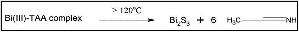
As discussed in our previous work,33 the solvothermal method provides a uniform heating environment under pressure, which results in more simultaneous nucleation than conventional methods. The solvents and precursors have an influence on the morphologies of the products and favor the synthesis of Bi2S3 with different pathways. The formation reaction may be described as follows.In solvothermal process, the reaction has been occurred in two steps. Bismuth(III) from BiCl3 solution coordinated with the TAA and a dimmer of bismuth(III) sulphide complex has been formed.34 The probable structure of the complex for bismuth(III) sulphide is presented in Scheme 1.
 | ||
| Scheme 1 The formation of dimmer of bismuth(III) sulfide complexes. | ||
During the reaction, at the initial stage, the decomposition occurs through the cleavage of the carbon–sulfur bond in Bi–TAA complex clusters and later on the formed Bi2S3 nuclei exhibits one dimensional growth and continue to grow along rod-shaped micelles via Ostwald ripening to form one-dimensional Bi2S3 nanorods or nanowire.
The possible reaction mechanism can be proposed as the following.
(i) The formation of dimmer of bismuth(III) sulphide complex or B(III)-TAA complexes via coordination reaction between the sulphur and the Bi(III) source at the initial stage of the solvothermal process.
(ii) Decomposition of bismuth(III) sulfide complex dimmer and the successive nucleation of Bi2S3 nanocrystals to form nuclei of Bi2S3 nanowires.
(iii) Formation of one-dimensional Bi2S3 nanowires originated from continuous growth of nuclei along rod-shaped micelles by Ostwald ripening.
Because of the sulfur-alkane structure, TAA is easily transformed into the resonance structure of allylmercaptan with relatively strong nucleophilicity through the resonance. The TAA coordinates to Bi3+ions to form bismuth(III) sulfide complex dimmer with relative stability in the form of allylmercaptan structure (Scheme 1), resulting in low generation rate of S2−. On the other hand, the bismuth(III) sulfide complexes dimmer also has a certain spatial orientation. These two factors are beneficial for the formation of uniform long Bi2S3 nanowires (Scheme 2). The CdS is also formed in the same fashion as discussed for Bi2S3. According to the Ksp of Bi2S3 (1.0 × 10−97) and CdS (8.0 × 10⁻²⁷), Bi2S3 will preferentially deposit and form crystal seeds before the formation of CdS. The PVP molecules could attach to some specific crystal facets of the seeds, which limits its growth along [211] direction, and finally confer Bi2S3 NWs. However, in the reaction system, the positively charged ions, such as Cd2+ and so forth, could weaken the affinity between PVP molecules and nanowires, promote their desorption from the surface of nanowire,35 and make the following epitaxial growth of CdS nanoparticles possible. Along with the prolonged reaction time, when Bi3+ was depleted after that there is an initiation of nucleation process of CdS. The as-produced CdS nanoparticles preferentially deposited at the surfaces of preformed Bi2S3 nanowires via epitaxial growth process to reduce their surface energy. Instead of a complete and uniform coating, isolated spherical CdS nanoparticles are formed at the surface of the Bi2S3 NWs. As the concentration of the Cd(NO3)2 increases, the size of decorated CdS nanoparticles also increased. The mobility of ions is quite hastier at higher concentration which leads into fast growth of nanoparticles. Hence, there is a secondary growth of the CdS on surface of Bi2S3 NWs as per standard crystal growth mechanism. The Scheme 3 represents the growth mechanism of Bi2S3 NWs and Bi2S3 NW decorated with CdS.
 | ||
| Scheme 2 Pyrolysis of bismuth(III) sulfide complexes dimmer. | ||
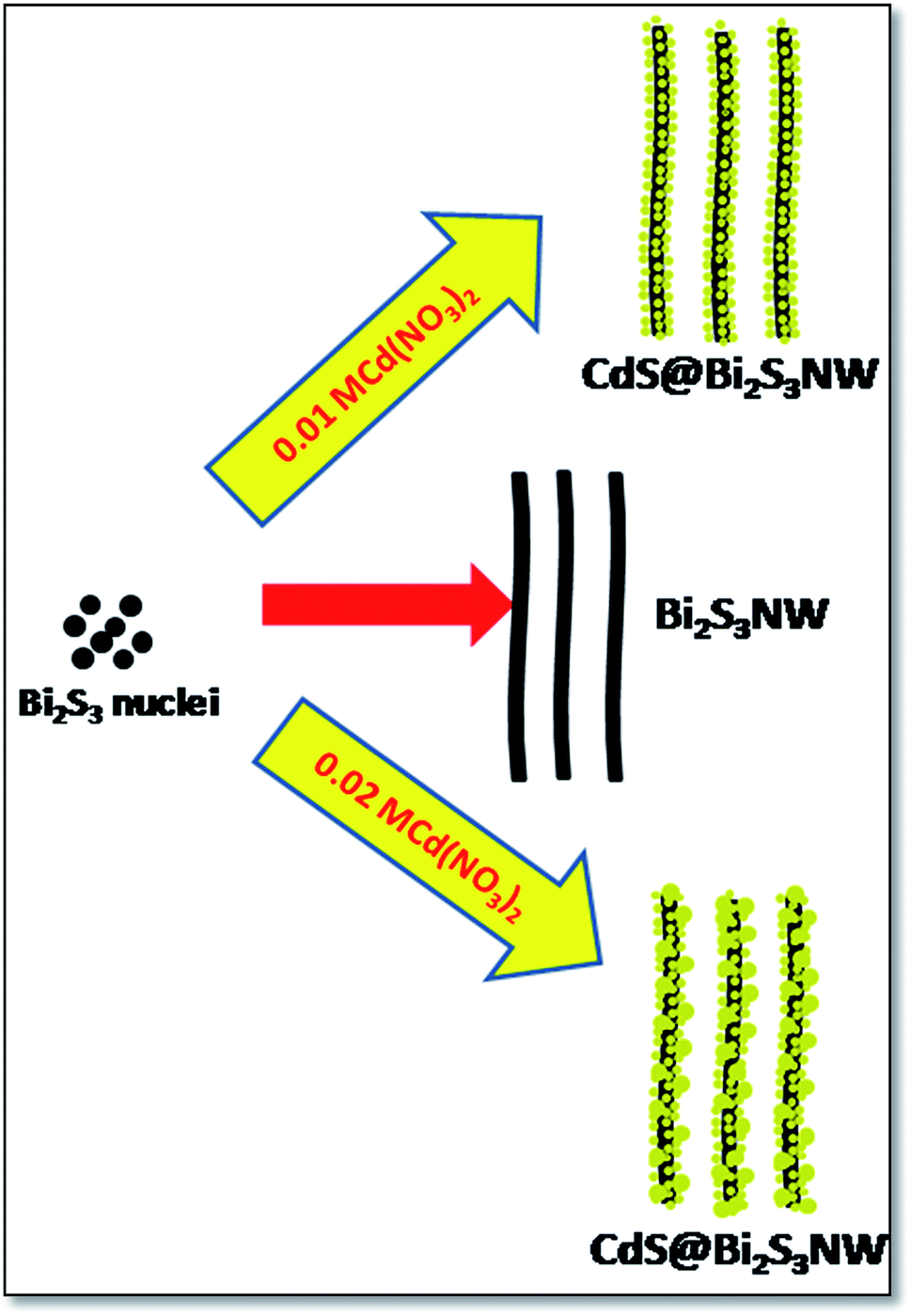 | ||
| Scheme 3 Schematic representation of growth mechanism of Bi2S3 NWs and Bi2S3 NW decorated with CdS. | ||
3.2 Photoresponse study
Fig. 6A shows the current–voltage (I–V) plot of prepared Bi2S3 NWs and Bi2S3 NW decorated with CdS in the dark and under irradiation with white light. Both of these nanostructures showed enhancement of the current flow under white light illumination, Bi2S3 NW decorated with CdS showed higher photo conductance. Upon irradiation at 300 W cm−2, the photocurrent increased approximately from 6.3 × 10⁻⁶ A cm−2 to 6.5 × 10⁻⁵ A cm−2 (10 times) for Bi2S3 NW decorated with CdS, whereas for Bi2S3, it increases from 1.10 × 10⁻⁴ to 1.45 × 10⁻⁴ A cm−2 (1.33 times) under similar conditions (at 1 V). This dramatic enhancement was further confirmed by the time dependent photoresponse measurements on both materials at 500 mV (bias voltage) by periodically turning the light on and off (Fig. 6B). We obtained considerably high photosensitivity. The current increased by 1 × 10⁻⁶ A and 15 × 10−6 A for Bi2S3 NW and Bi2S3 W decorated with CdS, respectively in response to the on-and-off operation for duration of 15 s. Even after a number of cycles, the photocurrent could still be changed by illumination switching; thus, the constructed device was fairly stable and reversible. | ||
| Fig. 6 Comparative I–V curves of the Bi2S3 NWa and Bi2S3 NW decorated with CdS (A) under dark and under light conditions. Time-dependent response of the devices measured in air at a bias of 100 mV. | ||
Bi2S3 NWs decorated with CdS prepared by the hydrothermal method creates more structural defects and surface states in materials than bare Bi2S3 NWs. Once a material with such defect energy levels is illuminated by light, the photo-generated carriers in it can efficiently be separated. Such spatial separation of the photo-generated carriers reduces the recombination rate of the electron–hole pairs, which in turn causes a significant increase of the carrier density, and thus produces a higher photocurrent.36,37
3.3 Photocatalytic hydrogen evolution via H2S splitting
Considering the good spectral response to solar light, the photocatalytic activities of Bi2S3 NWs and Bi2S3 NWs decorated with CdS nanoparticles for hydrogen evolution from H2S under solar light have been investigated. Different series of experiments were performed to compare the rate of hydrogen evolution by prepared samples and these results are summarized in Table 1 and Fig. 7. The maximum hydrogen evolution (4560 μmol h−1 0.5 g) has been obtained using Bi2S3 NWs decorated with CdS nanoparticles using 0.01 mol of Cd(NO3)2 which is higher than that of the Bi2S3 NWs (3000 μmol h−1 0.5 g) and Bi2S3 NWs decorated with CdS nanoparticles using 0.02 mol of Cd(NO3)2 (4140 μmol h−1 0.5 g), respectively. However, Bi2S3 NWs decorated with CdS nanoparticles using 0.01 mol of Cd(NO3)2 resulted in slightly higher (10%) hydrogen evolution compared with sample Bi2S3 NWs decorated with CdS nanoparticles using 0.02 mol of Cd(NO3)2. Both samples contain CdS nanoparticles interfaced with Bi2S3 NWs structures and have good hydrogen evolution. However, slightly lower activity in case of heterostructure prepared using 0.02 mol of Cd(NO3)2 is due to the larger CdS particles. The reusability of the Bi2S3 NWs decorated with CdS nanoparticles using 0.01 mol of Cd(NO3)2 as a catalyst for hydrogen generation via H2S splitting has been tested at same reaction conditions (See ESI III†). From reusability study, we conclude that our material is more stable after photocatalytic reaction. Surprisingly, it is observed the that the rate of hydrogen generation is higher than the pure CdS nanoparticles and commercial P25.38–40| Catalyst | Hydrogen evolution rate (μmol h−1 0.5 g) |
|---|---|
| Bi2S3 NW | 3000 |
| Bi2S3 NWs decorated with CdS nanoparticles using 0.01 mol of Cd(NO3)2 4H2O | 4560 |
| Bi2S3 NWs decorated with CdS nanoparticles using 0.02 mol of Cd(NO3)2 4H2O | 4140 |
 | ||
| Fig. 7 Time dependent hydrogen evolution using Bi2S3 NW decorated with CdS using 0.01 mol of Cd(NO3)2 (a), Bi2S3 NW decorated with CdS using 0.02 mol of Cd(NO3)2 (b) and Bi2S3 NW (c). | ||
The mechanism of evaluation of hydrogen gas via H2S splitting is discussed in our previous article in detail.33 In 0.5 M KOH solution, the weak diprotic acid, H2S dissociates and maintains equilibrium with the hydrogen disulfide (HS−) ions. The sulphide semiconductors absorb light and generate electron–hole (e−–h+) pairs. The valence band hole (hVB+) photogenerated after the band gap excitation of the Bi2S3 powder oxidizes the HS− ion to the disulfide ion (S2−2), liberating a proton from the HS− ion. The conduction band electron (eCB−) from the Bi2S3 photocatalyst reduces the protons to produce molecular hydrogen.41
| H2S + OH− ↔ 4HS− + H2O |
| Semiconductor invisible light: Bi2S3 or Bi2S3/CdS ↔ hVB+ + eCB− |
| Oxidation reaction: 2HS− + 2hVB+ → S22− + 2H+ |
| Reduction reaction: 2H+ + 2eCB− → H2 |
3.4 Hydrogen generation via glycerol degradation
Photocatalytic hydrogen evolution study was performed using Bi2S3 NWs and Bi2S3 NWs decorated with CdS catalysts from aqueous glycerol (50% solution) under visible light irradiation. Fig. 8 shows the effect of morphology on photocatalytic hydrogen evolution from glycerol. Utmost hydrogen generation i.e. 4.38 mmol h−1 g−1 was observed to be for the Bi2S3 NWs decorated with CdS nanoparticles using 0.01 mol of Cd(NO3)2 4H2O and 2.34 mmol h−1 g−1 for Bi2S3 NWs. The Bi2S3 NWs decorated with CdS showed high hydrogen evaluation rate than Bi2S3 NWs which may be due to the high surface area and improved charge carrier separation inside the composite i.e. Bi2S3 NWs decorated with CdS which ultimately support the enhanced photocatalytic activity. The reason for enhanced photocatalytic activity is already described in above section. | ||
| Fig. 8 Hydrogen production as a function of irradiation time using Bi2S3 NWs and Bi2S3 NWs decorated with CdS. | ||
Photocatalytic production of hydrogen from glycerol–water mixture consists of two distinct mechanisms, that is, photo-splitting of water and photo-reforming of glycerol.42 First, glycerol is oxidized, and then, it produces several intermediate compounds followed by hydrogen as product. Second, glycerol acts as sacrificial agent in photocatalytic water splitting.43 Glycerol, which acts as a sacrificial electron donor, is to rapidly remove the photo-generated holes (hydroxyl radicals) and/or photo-generated oxygen in an irreversible fashion, thereby suppressing electron–hole recombination and/or H2–O2 back reaction. By doing so, glycerol is progressively oxidized toward CO2, with intermediate formation of partially oxidized products. When complete oxidation of glycerol (and reaction intermediates) is achieved, oxygen can no longer be removed from the photocatalyst surface and the rate of hydrogen production drops to steady-state values comparable to those obtained in the absence of glycerol in solution.
The overall process, which may be described as photo-induced reforming of glycerol at room temperature, can be expressed by the following equation, which predicts the observed H2![[thin space (1/6-em)]](https://www.rsc.org/images/entities/char_2009.gif) :CO2 = 7:3 molar ratio of products formed:
:CO2 = 7:3 molar ratio of products formed:
| C3H8O3 + 3H2O → 3CO2 + 7H2 | (2) |
3.5 Photocatalytic methylene blue degradation
Methylene blue (MB) dye is used in textile industries massively and hence is of the major source of water pollution. Characteristic absorption peak of methylene blue appears at around 663. This absorption peak have been used to monitor the photocatalytic degradation process.44,45 The photodegradation efficiencies of MB mediated by the Bi2S3 NWs and Bi2S3 NWs decorated with CdS nanoparticles as photocatalyst as well as without photocatalyst under visible-light illumination (λ > 400 nm) are displayed in Fig. 9. Fig. 8 also shows the ln(C/C0) as a function of time under visible light (λ > 400 nm) irradiation, where C is the concentration of MB at the irradiation time t and C0 is the concentration in the adsorption equilibrium of the photocatalysts before irradiation. The degradation rate of dyes is expressed as degradation-rate constant k which is summarized in Table 2. | ||
| Fig. 9 Photocatalytic degradation of MB (initial concentration 1.0 × 10⁻⁵ M) using Bi2S3 NW decorated with CdS using 0.01 mol of Cd(NO3)2 (a), Bi2S3 NW decorated with CdS using 0.02 mol of Cd(NO3)2 (b), Bi2S3 NW (c) and without catalyst. | ||
| Catalyst | Rate constant (k) |
|---|---|
| Bi2S3 NWs | −0.042 |
| Bi2S3 NW decorated with CdS using 0.01 mol of Cd(NO3)2 | −0.094 |
| Bi2S3 NW decorated with CdS using 0.02 mol of Cd(NO3)2 | −0.065 |
| Without catalyst | 0.002 |
Rate constant obtained for different nanostructures indicates that the photocatalytic performances are strongly dependent on shape, size, and structure. The Bi2S3 NW decorated with CdS using 0.01 mol of Cd(NO3)2 showed higher photocatalytic activity for the degradation of MB Bi2S3 NWs as well as Bi2S3 NW decorated with CdS using 0.02 mol of Cd(NO3)2 as shown in Fig. 9 and Table 2. The enhanced photocatalytic activity Bi2S3 NWs decorated with CdS nanoparticles can be attributed due to creation of more the structural defects and surface states in materials than bare Bi2S3 NWs.
Fig. SI–IV (See EIS IV†) reveals the temporal evolution of the absorption spectra of an MB aqueous solution catalysed by the Bi2S3 NWs and Bi2S3 NWs decorated with CdS under visible light irradiation (λ > 400 nm).
3.6 Possible mechanism of the enhancement of photocatalytic activity of Bi2S3 NWs decorated with CdS photocatalyst
It is well reported that the photocatalytic activity is depend of some vital factors such as optical absorption, adsorption ability, phase structure and separation efficiency of photo-generated charge carriers.46,47 However, it is necessary to find out the band edge positions of the valence band (VB) and conduction band (CB) of both Bi2S3 and CdS to understand the photocatalytic reaction mechanism because they have strong relation with the photocatalytic redox process. The valence band potentials and conduction band potential of Bi2S3 and CdS were calculated according to the following empirical equations:48
 | (3) |
 | (4) |
Based on above values and our photocatalysis results, a possible mechanism for enhanced photocatalytic activity based on photo-carrier transfer is shown in Scheme 4.
 | ||
| Scheme 4 Schematic representation of photocatalytic hydrogen generation using Bi2S3 NWs decorated with CdS nanoparticles. | ||
In the presence of solar light irradiation, both Bi2S3 and CdS with band gap 1.37 and 2.40 eV can be photo-excited up to higher potential edge i.e. −1.53 and −1.31 eV for Bi2S3 and CdS due to the higher photon energy.52,53 However, bare Bi2S3 NWs nanorods show poor photocatalytic activity on expenses of the high recombination of the photoinduced carriers. In the case of Bi2S3 NWs decorated with CdS, due to higher conduction band potential (ECB) of Bi2S3 NWs compared to that of CdS, the transfer of the photo-excited electrons from the surface of Bi2S3 NWs to CdS nanoparticles take place. Simultaneously, the photo-excited holes created by the visible light irradiation on CdS can also migrate to the Bi2S3 NWs surface and react with the HS-ions. This transfer of electron–hole subsequently reduces the recombination of electrons and holes. The reduction of recombination admits more chances for electrons to participate in the reduction reaction to form H2 molecules which leads to a higher photocatalytic activity and excellent stability. Yet, with an increase in the amount of CdS, the excessive photoinduced electrons and holes can unavoidable recombine thus, decrease the photoactivity. The recombination of electron hole pair is also discussed in photoluminescence study. The optimized Bi2S3 NWs decorated with CdS prepared using 0.1 M Cd(NO3)2 which showed the best photocatalytic activity.
4. Conclusions
In nutshell, Bi2S3 NWs decorated with CdS nanoparticles have been successfully synthesized in solution phase at mild temperature. The growth mechanism of the formation of the nanoscale heterostructure has also been discussed. The prepared nanoscale heterostructure exhibits superior photocatalytic hydrogen generation activity and is strongly dependent on its composition and microstructure. Experimental studies reveal that the size of the CdS nanoparticle determines the band gap energy of the nanoscale heterostructure, controlling the charge carrier transition, recombination and separation in heterostructure. Hence the Bi2S3 NWs decorated with CdS showed an efficient hydrogen generation rate than bare Bi2S3 NWs. The enhanced photocatalytic results indicate potential application of nanoscale chalcogenide heterostructures in organic waste degradation. The methodology can also be extended to the preparation of other nanoscale heterostructures.Acknowledgements
The authors would like to thank, Executive Director, C-MET, Pune for technical support and DeitY, New Delhi financial support.Notes and references
- H. Li, J. Yang, J. Zhang and M. Zhou, RSC Adv., 2012, 2, 6258 RSC.
- X. H. Lu, G. M. Wang, T. Zhai, M. H. Yu, J. Y. Gan, Y. X. Tong and Y. Li, Nano Lett., 2012, 12, 1690 CrossRef CAS PubMed.
- B. Cheng, G. Wu, Z. Ouyang, X. Su, Y. Xiao and S. Lei, ACS Appl. Mater. Interfaces, 2014, 6, 4057 CAS.
- L. Li, Y. W. Yang, G. H. Li and L. D. Zhang, Small, 2006, 2, 548 CrossRef CAS PubMed.
- L. Hu, J. Yan, M. Liao, H. Xiang, X. Gong, L. Zhang and X. Fang, Adv. Mater., 2012, 24, 2305 CrossRef CAS PubMed.
- S. Liu, J. F. Ye, Y. Cao, Q. Shen, Z. F. Liu, L. M. Qi and X. F. Guo, Small, 2009, 5, 2371 CrossRef CAS PubMed.
- X. Zhang, Y. Liu and Z. Kang, ACS Appl. Mater. Interfaces, 2014, 6, 4480 CAS.
- Y.-C. Pu, G. Wang, K.-D. Chang, Y. Ling, Y.-K. Lin, B. C. Fitzmorris, C.-M. Liu, X. Lu, Y. Tong, J. Z. Zhang, Y.-J. Hsu and Y. Li, Nano Lett., 2013, 13, 3817 CrossRef CAS PubMed.
- X. Zhang, Y. Liu and Z. Kang, ACS Appl. Mater. Interfaces, 2014, 6, 4480 CAS.
- Z.-Q. Liu, W.-Y. Huang, Y.-M. Zhang and Y.-X. Tong, CrystEngComm, 2012, 14, 8261 RSC.
- H.-P. Jiao, X. Yu, Z.-Q. Liu, P.-Y. Kuang and Y.-M. Zhang, RSC Adv., 2015, 5, 16239 RSC.
- M. Hara, G. Hitoki, T. Takata, J. N. Kondo, H. Kobayashi and K. Domen, Catal. Today, 2003, 78, 555 CrossRef CAS.
- X. Zong, H. J. Yan, G. P. Wu, G. J. Ma, F. Y. Wen, L. Wang and C. Li, J. Chem. Soc. C, 2008, 130, 7176 CAS.
- W. Li, S. Xie, M. Li, X. Ouyang, G. Cui, X. Lu and Y. Tong, J. Mater. Chem. A, 2013, 1, 4190 CAS.
- P. Tongying, F. Vietmeyer, D. Aleksiuk, G. J. Ferraudi, G. Krylova and M. Kuno, Nanoscale, 2014, 6, 4117 RSC.
- P. Tongying, V. V. Plashnitsa, N. Petchsang, F. Vietmeyer, G. J. Ferraudi, G. Krylova and M. Kuno, J. Phys. Chem. Lett., 2012, 3, 3234 CrossRef CAS PubMed.
- H. Kim, M. Seol, J. Lee and K. Yong, J. Phys. Chem. C, 2011, 115, 25429 CAS.
- Z. Fang, Y. Liu, Y. Fan, Y. Ni, X. Wei, K. Tang, J. Shen and Y. Chen, J. Phys. Chem. C, 2011, 115, 13968 CAS.
- J. S. Jang, H. G. Kim, U. A. Joshi, J. W. Jang and J. S. Lee, Int. J. Hydrogen Energy, 2008, 33, 5975 CrossRef CAS.
- J. Hou, C. Yang, Z. Wang, S. Jiao and H. Zhu, RSC Adv., 2012, 2, 10330 RSC.
- X. Wang, G. Liu, Z.-G. Chen, F. Li, L. Wang, G. Q. Lu and H.-M. Cheng, Chem. Commun., 2009, 3452 RSC.
- Z. Fang, Y. Liu, Y. Fan, Y. Ni, X. Wei, K. Tang, J. Shen and Y. Chen, J. Phys. Chem. C, 2011, 115, 13968 CAS.
- A. Jana, C. Bhattacharya and J. Datta, Electrochim. Acta, 2010, 55, 6553 CrossRef CAS.
- X. He, L. Gao, S. Yang and J. Sun, CrystEngComm, 2010, 12, 3413 RSC.
- K. M. Gadave, C. D. Lokhande and P. P. Hankare, Mater. Chem. Phy.s, 1994, 38, 393–397 CrossRef CAS.
- N. Soltania, E. Saiona, W. M. M. Yunusa, M. Navaserya, G. Bahmanrokha, M. Erfania, M. R. Zareb and E. Gharibshahia, Sol. Energy, 2013, 97, 147 CrossRef.
- F. Zhang and S. S. Wong, Chem. Mater., 2009, 21, 4541 CrossRef CAS.
- T. Wu, X. G. Zhou, H. Zhang and X. H. Zhong, Nano Res., 2010, 3, 379 CrossRef CAS.
- Y. I Kim, S. J. Atherton, E. S. Brigham and T. E. Mallouk, J. Phys. Chem. B, 1993, 97, 11802 CrossRef.
- A. B. Murphy, J. Phys. D: Appl. Phys., 2006, 39, 3571 CrossRef CAS.
- R. P. Panmand, Y. A. Sethi, S. R. Kadam, M. S. Tamboli, L. K. Nikam, J. D. Ambekar, C.-J. Park and B. B. Kale, CrystEngComm, 2015, 17, 107 RSC.
- N. S. Chaudhari, S. S. Warule, S. A. Dhanmane, M. V. Kulkarni, M. Valant and B. B. Kale, Nanoscale, 2013, 5, 9383 RSC.
- U. V. Kawade, R. P. Panmand, Y. A. Sethi, M. V. Kulkarni, S. K. Apte, S. D. Naik and B. B. Kale, RSC Adv., 2014, 4, 49295 RSC.
- W. Xiang, Y. Yang, J. Yang, H. Yuan, J. An, J. Wei and X. Liu, J. Mater. Re.s, 2014, 29, 2272 CrossRef CAS.
- A. Z. Zelikin, G. K. Such, A. Postma and F. Caruso, Biomacromolecules, 2007, 8, 2950 CrossRef CAS PubMed.
- W. Tian, C. Zhang, T. Zhai, S.-L. Li, X. Wang, J. Liu, X. Jie, D. Liu, M. Liao, Y. Koide, D. Golberg and Y. Bando, Adv. Mater., 2014, 26, 3088 CrossRef CAS PubMed.
- C. Zhang, W. Tian, Z. Xu, X. Wang, J. Liu, S.-L. Li, D.-M. Tang, D. Liu, M. Liao, Y. Bando and D. Golberg, Nanoscale, 2014, 6, 8084–8090 RSC.
- B. B. Kale, J.-O. Baeg, S. K. Apte, R. S. Sonawane, S. D. Naik and K. R. Patil, J. Mater. Chem., 2007, 17, 4297–4303 RSC.
- S. N. Garaje, S. K. Apte, S. I. D. Naik, J. D. Ambekar, R. S. Sonawane, M. V. Kulkarni, A. Vinu and B. B. Kale, Environ. Sci. Technol., 2013, 47, 6664–6672 CAS.
- N. S. Chaudhari, S. S. Warule, S. A. Dhanmane, M. V. Kulkarni, M. Valant and B. B. Kale, Nanoscale, 2013, 5, 9383–9390 RSC.
- B. B. Kale, J. O. Baeg, K. Kong, S. Moon, L. K. Nikam and K. R. Patil, J. Mater. Chem., 2011, 21, 2624 RSC.
- J. Jitputti, Y. Suzuki and S. Yoshikawa, Catal. Commun., 2008, 9, 1265 CrossRef CAS.
- V. Gombac, L. Sordelli, T. Montini, J. J. Delgado, A. Adamski, G. Adami, M. Cargnello, S. Bernal and P. Fornasiero, J. Phys. Chem. A, 2010, 114, 3916 CrossRef CAS PubMed.
- Z. Liu, F. Chen, Y. Gao, Y. Liu, P. Fang and S. Wang, J. Mater. Chem. A, 2013, 1, 7027 CAS.
- G. Zhao, S. Liu, Q. Lu and L. Song, Ind. Eng. Chem. Res., 2012, 51, 10307 CrossRef CAS.
- I. Aslam, C. Cao, M. Tanveer, M. H. Farooq, W. S. Khan, M. Tahir, F. Idrees and S. Khalid, RSC Adv., 2015, 5, 60190 Search PubMed.
- J. Xu, M. Chen and Z. Wang, Dalton Trans., 2014, 43, 3537 RSC.
- Y. Xu and M. A. Schoonen, Am. Mineral., 2000, 85, 543 CrossRef CAS.
- Y. Yan, Z. Zhou, W. Li, Y. Zhu, Y. Cheng, F. Zhao and J. Zhou, RSC Adv., 2014, 4, 38558 RSC.
- L. Wang and W. Wang, CrystEngComm, 2012, 14, 3315 RSC.
- R. G. Pearson, Inorg. Chem., 1988, 27, 734 CrossRef CAS.
- J. Chen, S. Qin, G. Song, T. Xiang, F. Xin and X. Yin, Dalton Trans., 2013, 42, 15133 RSC.
- M. R. Gholipour, C.-T. Dinh, F. Bélandb and T.-O. Do, Nanoscale, 2015, 7, 8187 RSC.
Footnote |
| † Electronic supplementary information (ESI) available. See DOI: 10.1039/c6ra01488g |
| This journal is © The Royal Society of Chemistry 2016 |