DOI:
10.1039/C6RA03904A
(Paper)
RSC Adv., 2016,
6, 56885-56891
Heterojunction Cr2O3/CuO:Ni photocathodes for enhanced photoelectrochemical performance†
Received
12th February 2016
, Accepted 14th May 2016
First published on 3rd June 2016
Abstract
Heterojunction p-type photoelectrodes consisting of chromium oxide (Cr2O3) and copper oxide (CuO)-doped nickel (Ni) were prepared using aerosol-assisted chemical vapour deposition (AACVD) and spin-coating. All samples were photoresponsive and showed a photocathodic current in 0.5 M Na2SO4 under simulated solar illumination. The photocathode with an optimal composition of 3 layers of CuO and 0.5% Ni showed an enhanced photoactivity relative to bare Cr2O3. Based on the optical characterization and the flatband potential calculation, the fabricated Cr2O3, Cr2O3/CuO and Cr2O3/CuO:Ni can absorb visible light, which enables the water reduction reaction. Moreover, electrochemical impedance spectroscopy revealed that the charge transfer resistance of Cr2O3/CuO:Ni was decreased. Thus, in the heterojunction structure, the photogenerated electrons in Cr2O3 were transferred to the CuO:Ni layer, which then contributes to a high photoactivity. The combined advantages of the two strategies (heterojunction and doping) provide favourable charge transport characteristics of the materials.
Introduction
Investigation of photoelectrochemical (PEC) water splitting has long been studied for renewable energy sources. Particularly, study is focussed on semiconductor materials, which have great potential in the splitting of water molecules into oxygen and hydrogen gas. Metal oxides have been chosen for decades to drive photocatalytic reactions. However, one major problem may arise from using metal oxides. Most of the metal oxides have a wide bandgap energy that cannot utilize sufficient solar photons to split water efficiently unless modifications are made to the corresponding photoelectrodes.1 Several attempts, including nanostructure morphology control,2,3 substitutional doping of metal cations4,5 and formation of the heterojunction,6,7 have been made to address this limitation in order to improve PEC performance. In contrast to a single component photocatalyst, a heterojunction of two semiconductors has been recognized as an attractive solution to create high efficiency devices by extending light absorption. This can combine the merits of each component to show synergistic effects.8,9 Additional benefits can be expected by creating a junction structure that can enhance electron–hole separation, preventing energy loss during electron transfer in the electrolyte.10 Ever since the pioneering work of an n-type TiO2 electrode by Fujima and Honda,11 numerous studies have primarily concentrated on n-type metal oxide semiconductors, such as BiVO4,12–15 Fe2O3 (ref. 16–19) and WO3,20–23 in photoelectrolysis. On the other hand, research efforts on p-type semiconductor photoelectrode materials, such as Co2O3,24,25 NiO,26,27 Cr2O3 (ref. 7 and 28) and CuO,29,30 have been seldom reported. Among these materials, Cr2O3 and CuO are the most promising materials to be applied in photoelectrodes. Cr2O3 has been studied extensively in the field of photocatalysis,31 homogeneous catalysis32 and hydrogen absorption.33 Under visible light irradiation, Cr2O3 exhibited weak photocatalytic activity due to its wide bandgap energy (3.45 eV),31 which allows this material only to be activated by UV light. Therefore, the formation of a heterojunction with matching band potentials is expected to improve the photo-conversion efficiency of photogenerated charge carriers. For p-type photoelectrode materials, CuO with a narrow bandgap energy (1.4–1.8 eV) was found to be much more active under visible light and has a suitable band position for the water reduction reaction (H+ to H2).4,34–37 Aside from that, CuO has long been a photocathode candidate because of several reasons including its low production cost, natural abundance, non-toxicity, good electrical properties and more importantly it can produce faster electron transfer compared to other photocatalysts.38
In the past years, some metal oxide semiconductors have been modified by forming a junction structure to promote efficient electron–hole separation. For example, ZnO/CuO heterojunction branched nanowire photoelectrodes have been found to exhibit a higher photocurrent due to a broadband photoresponse from ultraviolet (UV) to the near infrared (IR) region.39 Recently, it has been shown that a higher photocatalytic activity could be obtained from a CuO/TiO2 heterojunction. The performance enhancement is attributed to the photoelectron transfer from the more negative conduction band of TiO2 to CuO.40 On top of that, due to the relatively high resistance of CuO, the movement of photon-excited electrons to the electrode and electrolyte interface may be limited.41 Hence, to reduce the resistance of CuO and to improve the photo-responsiveness of CuO, doping with metal ions is one solution.41 Doping the semiconductor with impurity metal ions is a useful technique to change the electrical, magnetic and optical properties of the material.42 Recently, Ni has received increasing interest as a dopant in studies on thin films.43–45 In a previous work, the electronic properties of CuO were altered by doping with Ni. An increase in the photocurrent density and conductivity by 0.76% and 1.5%, respectively, was realized after 2% of Ni concentration was added as a dopant into CuO.5 Therefore, we can say that incorporation of Ni ions into CuO nanostructures can affect the conductivity of the host material, depending on the amount of dopant inserted. Herein, we applied both the concepts of heterojunction and doping as useful approaches to enhance the PEC properties. First, we fabricated the heterojunction Cr2O3/CuO thin film photocathodes through aerosol-assisted chemical vapour deposition (AACVD) and spin-coating. In a separate experiment, Ni dopant was added into a CuO sol–gel, which later was coated on Cr2O3 through spin-coating. These two strategies were combined together in order to better utilize solar irradiation to improve the photocatalytic activity. Structural characterization was carried out and the PEC behavior of the fabricated samples was also examined.
Experimental
Deposition of Cr2O3 thin films by AACVD
Conducting glass of fluorine-doped tin oxide (FTO, TEC 8, ∼8 Ω sq−1 Pilkington) was cleaned with acetone, iso-propanol and deionized water for 15 minutes successively in an ultrasonic bath and then dried in air. To prepare Cr2O3 by AACVD, modification of a previously published method was employed.12 An ultrasonic dehumidifier was used to generate the aerosol from a mixture of 50 mM chromium(III) acetylacetonate, Cr(C5H7O2)3 in 100 ml toluene, which was then transported by a carrier gas to the heated substrate (∼460 °C). The deposition time was optimized from 15, 30, 45 and 60 minutes. The as-deposited Cr2O3 thin films are greenish, uniform and adhere strongly onto the FTO substrate as tested by the “scotch tape test”.
Synthesis of the sol–gel Ni-doped CuO solution
All the CuO layers were prepared based on a previously published method with some modifications.30 To prepare the 0.3 M CuO sol, copper(II) acetate monohydrate, Cu(CO2CH3)2·H2O was added in ethanol under vigorous stirring for 20 minutes. At this time, diethanolamine was dripped slowly until the solution was completely dissolved. Subsequently, a minimum amount of propylene glycol was added into the solution and then stirred for 60 minutes. The solution was allowed to age for 2 days at room temperature. 10 mM nickel(II) nitrate hexahydrate, Ni(NO3)2·6H2O in a minimum amount of ethanol was prepared as the dopant. Then, 0.25%, 0.5% and 1% of the Ni solution was dripped into CuO sol and stirred in an ultrasonic bath before use.
CuO:Ni layer deposition
The as-prepared CuO and CuO:Ni sol were spin coated (1500 rpm, 25 seconds) onto Cr2O3 films and then dried in air at 100 °C for 15 minutes for each coating to remove the organic solvent. This process was repeated three times before the substrates were subjected to a final thermal annealing at 450 °C for 1 hour.
Materials characterization
Structural and optical characterizations. X-ray diffraction (XRD) spectra were obtained using the model Bruker D8 Advance in the range of 20 to 60°. The average grain size of the samples was calculated based on the following Scherrer equation:
where λ is the X-ray wavelength of 0.15406 nm, β is the full width at half-maximum (FWHM) at (110) for Cr2O3 and (111) for Cr2O3/CuO and Cr2O3/CuO:Ni, respectively, θ is the Bragg angle and k is a constant. The surface roughness and topographic images of the thin films were identified using NanosurfeasyScan 2 Atomic Force Microscopy (AFM). For ultraviolet-visible spectroscopy (UV-vis) absorbance studies, samples were measured using a PerkinElmer UV/VIS/NIR spectrophotometer Lambda 950. The thin film morphology was characterized using field-emission scanning electron microscopy (FESEM) and energy dispersive X-ray spectroscopy (EDX) on FE-SEM SUPRA VP55.
PEC measurements. The steady-state photocurrent density and electrochemical impedance spectroscopy (EIS) as well as Mott–Schottky analysis were performed in a 3-electrode configuration consisting of saturated calomel electrode (SCE) (saturated KCl) as the reference electrode, a Pt plate as the counter electrode and the Cr2O3, Cr2O3/CuO, Cr2O3/CuO:Ni thin films as the working electrodes. The samples were measured in a 0.5 M Na2SO4 aqueous electrolyte solution with 1 cm2 of active area. A Metrohm potentiostat/galvanostat Autolab PGSTAT 204 was used to supply the desired potential and frequency to the electrodes. The measurements were conducted in dark, chopped and light conditions with a xenon lamp (with a light intensity of 100 mW cm−2). The EIS and Mott–Schottky characterizations were performed using the same experimental setup as above. The applied frequency for EIS was 100 kHz to 10 mHz under dark and illumination. The Mott–Schottky plots were performed in the absence of light at −0.5 to 0.4 V vs. SCE.
Results and discussion
Structural properties
Structural characteristics of the as-deposited Cr2O3, Cr2O3/CuO and Cr2O3/CuO:Ni films analysed using XRD are presented in Fig. 1. For Cr2O3 (Fig. 1a), the peaks at 24.5°, 33.6°, 36.2°, 41.5°, 50.2° and 54.8° correspond to the (012), (104), (110), (113), (024) and (116) planes. All the Cr2O3 peaks on the XRD pattern can be indexed to the rhombohedral structure (JCPDS 70-3765). After CuO was coated on the Cr2O3 layer (Fig. 1b), new peaks were observed at 32.5°, 35.6°, 38.8° and 48.7°. These peaks are attributed to the (110), (−111), (111) and (−202) planes, which represent a CuO base-centered monoclinic structure (JCPDS 73-6023). The XRD pattern of Cr2O3/CuO:Ni (Fig. 1c) has the same crystal structure as that of Cr2O3/CuO except that the new peaks of Ni appear at the planes (111) and (200). The other peaks showed no significant changes, suggesting that the mass loading of Ni is very small. In addition, the reduction of the grain size observed in Table 1 is attributed to the lattice distortion induced by Ni doping.46 From XRD analysis, the formation of Cr2O3, CuO and Ni was confirmed and no impurity peaks were detectable.
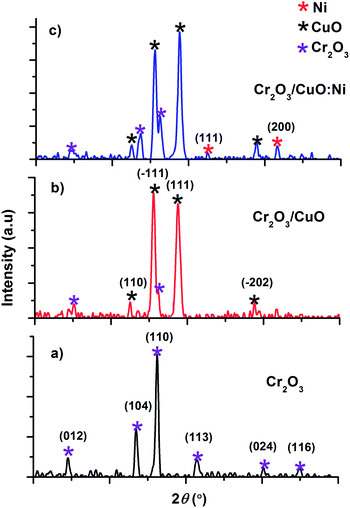 |
| | Fig. 1 XRD patterns of (a) Cr2O3, (b) Cr2O3/CuO and (c) the Cr2O3/CuO:Ni thin films. | |
Table 1 Surface roughness (obtained from AFM), grain size (calculated from XRD) and particle size (taken from FESEM) of the Cr2O3, Cr2O3/CuO, and Cr2O3/CuO:Ni thin films
| Samples |
Grain size (Å) |
Surface roughness (nm) |
Particle size (nm) |
| Cr2O3 |
453.10 |
45.64 |
840.00 |
| Cr2O3/CuO |
283.90 |
49.59 |
94.12 |
| Cr2O3/CuO:Ni |
209.60 |
54.56 |
58.83 |
AFM
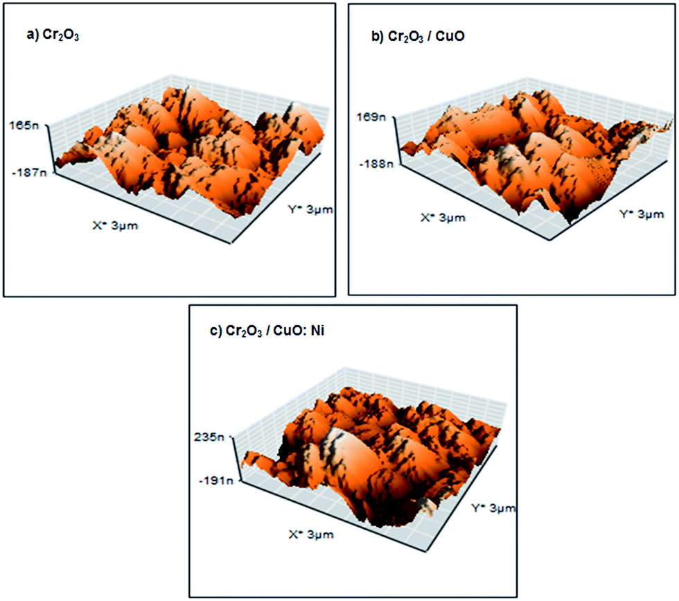
The surface roughness and grain size of each sample were compared and are presented in Table 1. Fig. 2 displays a 3D view of the thin films. Although the AFM images show less noticeable changes in the thin film topology, Cr2O3/CuO:Ni recorded the highest surface roughness and smallest grain size compared to Cr2O3 and Cr2O3/CuO. Hence, this indicates that the formation of the CuO:Ni layer onto Cr2O3 alters the topology of the films. Generally, high surface roughness and small grain size can significantly affect the PEC performance as more sites are exposed in the photocatalytic reaction. It was found that the grain size of the films decreased in the presence of Ni. The reduction of grain size is attributed to the substitution of Ni2+ (0.69 Å) with Cu2+ (0.73 Å) onto the CuO lattice, which further causes lattice distortion and a change in ionic radii.45
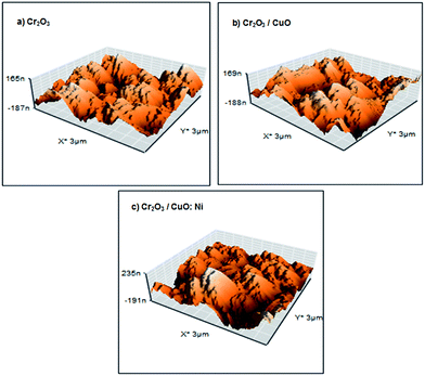 |
| | Fig. 2 AFM images of the (a) Cr2O3, (b) Cr2O3/CuO and (c) Cr2O3/CuO:Ni thin films. | |
Morphological properties
Elemental and topographical characteristic of the thin films were determined through FESEM and the results are shown in Fig. 3.
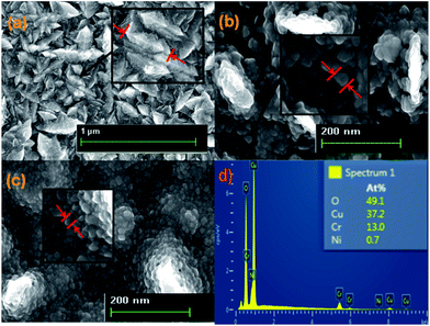 |
| | Fig. 3 FESEM images of (a) Cr2O3, (b) Cr2O3/CuO and (c) Cr2O3/CuO:Ni and (d) EDX of the Cr2O3/CuO:Ni thin film photocathode. | |
Cr2O3 thin films grown over the substrate exhibited a stone-like structure (Fig. 3a). Whereas, after being coated by a CuO layer, the surface morphology of the Cr2O3/CuO thin films revealed a porous surface with some large particles appearing to have a plate-like shape. The same porous structure was also recorded for Cr2O3/CuO:Ni. This structure can improve the electrode/electrolyte interfacial area. As charges are generated at the electrolyte interface, the photogenerated holes have to travel through less bulky material. As a result, the chance of recombination can be reduced during the photo-oxidation reactions.47 In the case of Cr2O3/CuO:Ni, more charges are generated than Cr2O3 and Cr2O3/CuO, thereby increasing the charge mobility. Moreover, after Ni was added into the CuO, most of the particles viewed in Fig. 3c have a small size compared to the particle size in Fig. 3b. This result is tabulated in Table 1. Note that the decrease in particle size observed in FESEM images is consistent with the XRD results calculated using Scherrer's equation. Furthermore, some of the particles seemed to agglomerate and form rougher surfaces consistent with the results obtained from AFM analysis. From the FESEM images, the thickness of the Cr2O3, Cr2O3/CuO and Cr2O3/CuO:Ni films were 0.88, 1.13 and 1.25 μm, respectively (Fig. S1†). The EDX image of Cr2O3/CuO:Ni (Fig. 3d) confirms the elemental existence of Cr, Cu, O and Ni.
Optical properties
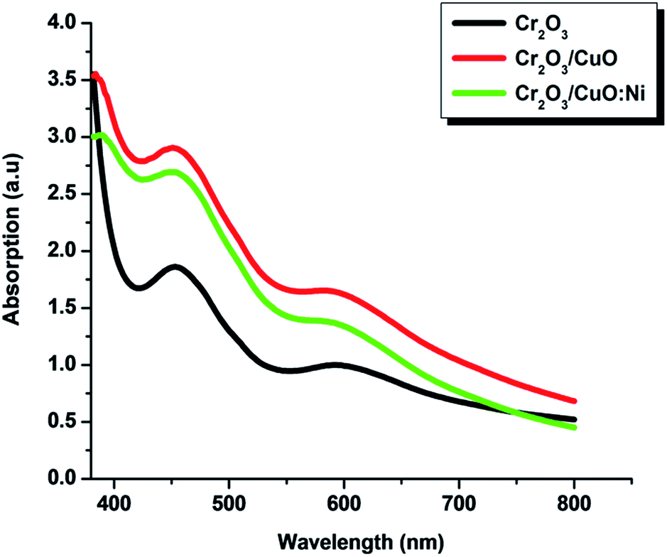
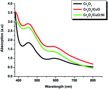
Optical absorption measurements of the Cr2O3, Cr2O3/CuO and Cr2O3/CuO:Ni thin films are shown in Fig. 4. Nearly similar peak patterns with absorption peaks at ∼450 and ∼600 nm were observed in all samples. The similar trend of Cr2O3 absorption is also consistent with the previous study.48 Note that, as for all the samples, the dominant peak was exhibited by Cr2O3, hence the peaks of CuO and Ni cannot be seen. Initially, Cr2O3 showed moderate light intensity, however, after layers of CuO and CuO:Ni were deposited on the Cr2O3 film, the light intensity increased by ∼10% and ∼15%, respectively. This suggests that the absorbance peaks of CuO and Ni fall in the same wavelength region of Cr2O3. Small differences in the absorption intensity of the Cr2O3/CuO and Cr2O3/CuO:Ni films may be attributed to the variation in thickness as well as scattering from different morphology of the deposited films.49
 |
| | Fig. 4 UV-vis spectrum of the Cr2O3, Cr2O3/CuO and Cr2O3/CuO:Ni thin films. | |
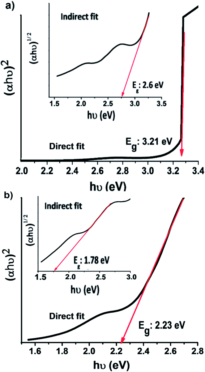
The optical bandgap energy of the samples was estimated from Tauc plots (Fig. 5). The best fit for the optical bandgap was found for the direct bandgap transition rather than the indirect transition. The bandgap energy estimated for Cr2O3 is 3.21 eV (Fig. 5a). This value is smaller than previously reported for its bulk counterpart (3.5 eV),31 which can be ascribed to the quantum confinement effect.50 It can be seen that the heterojunction Cr2O3/CuO:Ni has a bandgap energy of 2.23 eV. The combination of CuO:Ni and Cr2O3 led to a decrease in the bandgap energy, which confirms the substitution of Cu2+ ions with Ni2+ ions in the host lattice. This facilitates an easy passage of electrons from the conduction band to the valence band as compared to the Cr2O3 sample.
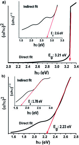 |
| | Fig. 5 Tauc plots of the (a) Cr2O3 and (b) Cr2O3/CuO:Ni thin films. | |
PEC characterization
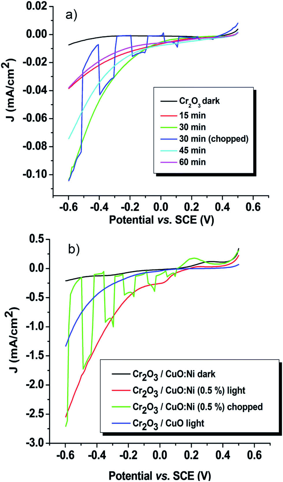
The PEC performance of the thin film photoelectrodes was determined in a 0.5 M Na2SO4 electrolyte between 0.5 and −0.6 V vs. SCE under dark and simulated conditions. As the potentials sweep from the positive to the negative direction, cathodic photocurrents were observed for all the samples. Moreover, the chopped pattern displays a good initial photocurrent spike. The photocurrent spike occurs before a sharp decay to a steady-state photocurrent, which generally is assigned to electron–hole recombination at immediate time or corrosive effects.51 An initial experiment was carried out to determine the optimum time to deposit Cr2O3. Fig. 6a shows the time-dependence of the photocurrent density of Cr2O3. Cr2O3 prepared for 30 minutes showed the highest performance with 0.1 mA cm−2 at −0.6 V vs. SCE. It is known that a short deposition time results in thinner films, whereas a longer deposition time corresponds to thicker films. As the film thickness increases, the sample produces a lower photocurrent density. This might be due to the greater distance travelled by the charge carriers, thereby increasing the rate of recombination of electron–hole pairs.51 On the contrary, the lowest photocurrent density recorded by the thinnest films (15 minutes) might be due to the shortest distance travelled by the charge carriers compared to its diffusion length. Thus, the charge carriers have not had enough time to diffuse to electron–hole pairs.
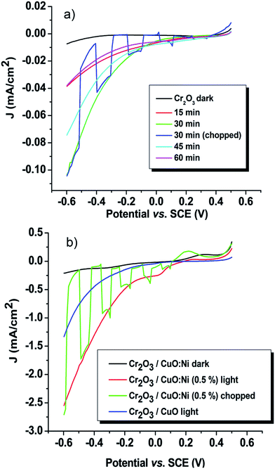 |
| | Fig. 6 The photocurrent density–potential curves of the (a) Cr2O3 and (b) Cr2O3/CuO:Ni (0.5%) thin film photocathodes. | |
The low photocurrent magnitude exhibited by Cr2O3 is due to its wide bandgap, thus limiting the electron excitation rate from the valence band to the conduction band.24 By coupling Cr2O3 with CuO and forming a heterojunction, the photocurrent density of Cr2O3 was increased from 0.1 to 1.33 mA cm−2. The photocurrent enhancement is assigned to the subsequent increase of minority carriers of electrons under illumination.51 In order to determine the improved property of Cr2O3, photocurrent measurements of single CuO and CuO:Ni were conducted under the same conditions (Fig. S2 and Table S1†). Interestingly, the results prove that the photocatalytic activity was enhanced in the heterojunction structure rather than in a single-layer thin film electrode. Further, a different percentage of Ni dopant was optimized in order to study its effect towards the conductivity of the prepared electrodes. Table 2 represents the photocurrent density as a function of Ni content at −0.6 V vs. SCE. The photocurrent density of Ni-doped CuO was enhanced as the amount of Ni increased from 0.25 to 0.5% and then decreased with 1% Ni. The Ni ions have a similar size to the Cu2+ ions, which means they can be more easily substituted into the CuO lattice.5 Therefore, the conductivity increased due to a higher concentration of carriers available (Cu2+ and Ni2+). Among other samples, the Cr2O3/CuO:Ni thin film photoelectrodes exhibited the higher photocurrent density of 2.6 mA cm−2. Based on the FESEM results, the effect of Ni doping appears to reduce the particle size, resulting in a large surface area for reaction.
Table 2 Photocurrent density of the Cr2O3, Cr2O3/CuO and Cr2O3/CuO:Ni photocathodes with a different percentage of Ni content
| Samples |
Ni content (%) |
Photocurrent density vs. SCE at −0.6 V (mA cm−2) |
| Cr2O3 (30 min) Cr2O3/CuO |
— |
0.10 |
| — |
1.33 |
| Cr2O3/CuO:Ni |
0.25 |
1.42 |
| 0.50 |
2.55 |
| 1.00 |
1.90 |
EIS was carried out under illumination at a bias potential of −0.2 V. The characteristics of charge transfer resistance Rct can be represented in the semicircle of the Nyquist plot. Clearly, a smaller arc radius was observed for Cr2O3/CuO:Ni compared to those of Cr2O3 and Cr2O3/CuO (Fig. 7). This suggests that the charge transfer resistance of Cr2O3 was reduced due to higher electron conductivity after the formation of the Ni-doped CuO heterojunction. In other words, the heterojunction of Cr2O3 with CuO:Ni promotes interfacial charge transport and facilitates photoinduced charge separation.52
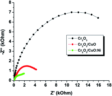 |
| | Fig. 7 Nyquist plots of all the samples under simulated 1 sun (air mass 1.5G, 100 mW cm−2). | |
Mott–Schottky plots for the Cr2O3 and CuO:Ni electrodes in 0.5 M Na2SO4 are displayed in Fig. 8a. The flatband potentials were determined from the intersection of the line fit to the 1/C2 with the x-axis. The flatband potentials of Cr2O3 and CuO:Ni were 0.6 and 0.7 V vs. SCE respectively. By converting the obtained flatband potential with respect to the normal hydrogen electrode (NHE), the calculated values were 0.84 and 0.94 V vs. NHE. Based on the optical bandgap energy (see Fig. 5 and S3†) and flatband potentials, we sketched the energy band diagram of the heterojunction Cr2O3/CuO:Ni in Fig. 8b. The conduction band and valence band of Cr2O3 are more negative than the corresponding bands of CuO:Ni. Therefore, this condition favours the facile injection of photogenerated electrons from the conduction band of Cr2O3 to that of CuO:Ni. When the photoelectrode is illuminated with simulated solar light, photogenerated charge carriers are generated at the conduction band of both Cr2O3 and CuO:Ni. The excited electrons in Cr2O3 migrate to the conduction band of CuO:Ni easily due to the potential difference and then accumulate with the existing photogenerated electrons of CuO:Ni. Finally, these electrons move to the semiconductor/electrolyte interface, whereas holes collect on FTO.
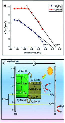 |
| | Fig. 8 Mott–Schottky plots of the (a) Cr2O3 and CuO:Ni thin film photocathodes. (b) Schematic representation of the Cr2O3 and CuO:Ni films in aqueous medium under illuminated conditions. | |
Conclusions
Cr2O3, Cr2O3/CuO and Cr2O3/CuO:Ni photocathodes were successfully prepared via AACVD and spin-coating. The PEC performance of these photoelectrodes was studied with a photocurrent density–voltage curve, EIS and Mott–Schottky analysis. The photoresponse of a single Cr2O3 photoelectrode increased after the formation of a heterojunction with CuO and Ni-doped CuO (CuO:Ni). Thin films with the composition Cr2O3 (30 minutes), a CuO layer and Ni content 0.5% gave the best photocurrent performance of 2.6 mA cm−2 vs. SCE at −0.6 V. In summary, combining these two strategies (heterojunction and doping) in a single photoelectrode may provide an effective way to enhance the PEC properties.
Acknowledgements
The authors would like to thank the Universiti Kebangsaan Malaysia for the financial support from grant ICONIC-2013-005.
Notes and references
- S. U. M. Khan, M. Al-Shahry and W. B. Ingler, Science, 2002, 27, 2243 CrossRef PubMed.
- I. S. Cho, Z. Chen, A. J. Forman, D. R. Kim, P. M. Rao, T. F. Jaramillo and X. Zheng, Nano Lett., 2011, 11, 4978 CrossRef CAS PubMed.
- K. S. Ahn, Y. Yan, S. Shet, K. Jones, T. Deutsch, J. Turner and M. Al-Jassim, Appl. Phys. Lett., 2008, 93, 163117 CrossRef.
- C.-Y. Chiang, Y. Shin and S. Ehrman, J. Electrochem. Soc., 2012, 159, B227 CrossRef CAS.
- C.-Y. Chiang, Y. Shin and S. Ehrman, Energy Procedia, 2014, 61, 1799 CrossRef CAS.
- J. Lin, P. Hu, Y. Zhang, M. Fan, Z. He, C. K. Ngaw, J. S. C. Loo, D. Liao and T. T. Y. Tan, RSC Adv., 2013, 3, 9330 RSC.
- Z. Hu, M. Xu, Z. Shen and J. C. Yu, J. Mater. Chem. A, 2015, 3, 14046 CAS.
- J. S. Jang, S. M. Ji, S. W. Bae, H. C. Son and J. S. Lee, J. Photochem. Photobiol., A, 2007, 188, 112 CrossRef CAS.
- Y. Tak, S. J. Hong, J. S. Lee and K. Yong, J. Mater. Chem., 2009, 19, 5945 RSC.
- S. J. Hong, S. Lee, J. S. Jang and J. S. Lee, Energy Environ. Sci., 2011, 4, 1781 CAS.
- A. Fujishima and K. Honda, Nature, 1972, 238, 37 CrossRef CAS PubMed.
- S. N. F. Mohd-Nasir, M. A. Mat-Teridi, M. Ebadi, J. S. Sagu, M. Y. Sulaiman, N. A. Ludin and M. A. Ibrahim, Phys. Status Solidi A, 2015, 212, 2910 CrossRef CAS.
- P. Brack, J. S. Sagu, T. A. N. Peiris, A. McInnes, M. Senili, K. G. U. Wijayantha, F. Marken and E. Selli, Chem. Vap. Deposition, 2015, 21, 41 CrossRef CAS.
- J. Yin, S. Huang, Z. Jian, Z. Wang and Y. Zhang, Mater. Sci. Semicond. Process., 2015, 34, 198 CrossRef CAS.
- J. A. Seabold, K. Zhu and N. R. Neale, Phys. Chem. Chem. Phys., 2014, 16, 1121 RSC.
- A. A. Tahir, M. A. Mat-Teridi and K. G. U. Wijayantha, Phys. Status Solidi RRL, 2014, 8, 976 CrossRef CAS.
- R. Rajendran, Z. Yaakob, M. Pudukudy, M. S. Abd-Rahaman and K. Sopian, J. Alloys Compd., 2014, 608, 207 CrossRef CAS.
- Y. S. Hu, A. Kleiman-Shwarsctein, A. J. Forman, D. Hazen, J. N. Park and E. W. McFarland, Chem. Mater., 2008, 20, 3803 CrossRef CAS.
- D. K. Zhong, J. Sun, H. Inumaru and D. R. Gamelin, J. Am. Chem. Soc., 2009, 131, 6086 CrossRef CAS PubMed.
- X. Liu, F. Wang and Q. Wang, Phys. Chem. Chem. Phys., 2012, 14, 7894 RSC.
- K. Sivula, F. Le Formal and M. Grätzel, Chem. Mater., 2009, 21, 2862 CrossRef CAS.
- W. Cristino, S. Caramori, R. Argazzi, L. Meda, G. L. Marra and C. A. Bignozzi, Langmuir, 2011, 27, 7276 CrossRef PubMed.
- B. Cole, B. Marsen, E. Miller, Y. Yan, B. To, K. Jones and M. Al-Jassim, J. Phys. Chem. C, 2008, 112, 5213 CAS.
- M. Ebadi, M. A. Mat-Teridi, M. Y. Sulaiman, W. J. Basirun, N. Asim, N. A. Ludin, M. A. Ibrahim and K. Sopian, RSC Adv., 2015, 5, 36820 RSC.
- J. He, Y. Peng, Z. Sun, W. Cheng, Q. Liu, Y. Feng, Y. Jiang, F. Hu, Z. Pan, Q. Bian and S. Wei, Electrochim. Acta, 2014, 119, 64 CrossRef CAS.
- M. A. Mat-Teridi, A. A. Tahir, S. Senthilarasu, K. G. U. Wijayantha, M. Y. Sulaiman, N. Ahmad-Ludin, M. A. Ibrahim and K. Sopian, Phys. Status Solidi RRL, 2014, 8, 982 CrossRef CAS.
- C. Hu, K. Chu, Y. Zhao and W. Y. Teoh, ACS Appl. Mater. Interfaces, 2014, 6, 18558 CAS.
- M. Gong, W. Zhou, M. J. Kenney, R. Kapusta, S. Cowley, Y. Wu, B. Lu, M.-C. Lin, D.-Y. Wang, J. Yang, B. J. Hwang and H. Da, Angew. Chem., 2015, 127, 12157 CrossRef.
- K. Nakaoka, J. Ueyama and K. Ogura, J. Electrochem. Soc., 2004, 151, C661 CrossRef CAS.
- Y.-F. Lim, C. S. Chua, C. J. J. Lee and D. Chi, Phys. Chem. Chem. Phys., 2014, 16, 25928 RSC.
- K. Maeda, K. Teramura, D. L. Lu, N. Saito, Y. Inoue and K. Domen, Angew. Chem., Int. Ed., 2006, 45, 7806 CrossRef CAS PubMed.
- R. Bhosale, S. Pujari, G. Muley, B. Pagare and A. Gambhire, J. Nanostruct. Chem., 2013, 3, 46 CrossRef.
- J. L. Bobet, S. Desmoulins-Krawiec, E. Grigorova, F. Cansell and B. Chevalier, J. Alloys Compd., 2003, 351, 217 CrossRef CAS.
- C.-Y. Chiang, M. H. Chang, H.-S. Liu, C. Y. Tai and S. Ehrman, Ind. Eng. Chem. Res., 2012, 51, 5207 CrossRef CAS.
- C. Y. Chiang, Y. Shin, K. Aroh and S. Ehrman, Int. J. Hydrogen Energy, 2012, 37, 8232 CrossRef CAS.
- C. Y. Chiang, K. Aroh and S. Ehrman, Int. J. Hydrogen Energy, 2012, 37, 4871 CrossRef CAS.
- C. Y. Chiang, K. Aroh, N. Franson, V. R. Satsang, S. Dass and S. Ehrman, Int. J. Hydrogen Energy, 2011, 36, 15519 CrossRef CAS.
- Y. S. Chaudhary, A. Agrawal, R. Shrivastav, V. R. Satsangi and S. Dass, Int. J. Hydrogen Energy, 2004, 29, 131 CrossRef CAS.
- A. Kargar, Y. Jing, S. J. Kim, C. T. Riley, X. Pan and D. Wang, ACS Nano, 2013, 7, 11112 CrossRef CAS PubMed.
- S. J. A. Moniz and J. Tang, ChemCatChem, 2015, 7, 1659 CrossRef CAS.
- C.-Y. Chiang, Y. Shin and S. Ehrman, Energy Procedia, 2014, 61, 1799 CrossRef CAS.
- S. Al-Amri, M. S. Ansari, S. Rafique, M. Aldhahri, S. Rahimuddin, A. Azam and A. Memic, Curr. Nanosci., 2015, 11, 191 CrossRef CAS.
- C.-Y. Chiang, Y. Shin and S. Ehrman, Appl. Energy, 2016, 164, 1039 CrossRef CAS.
- S. Al-Amri, M. S. Ansari, S. Rafique, M. Aldhahri, S. Rahimuddin, A. Azam and A. Memic, Curr. Nanosci., 2015, 11, 191 CrossRef CAS.
- S. Baturay, A. Tombak, D. Kaya, Y. Selim Ocak, M. Tokus, M. Aydemir and T. Kilicoglu, J. Sol-Gel Sci. Technol., 2016, 78, 422 CrossRef CAS.
- S. Mehraj, M. S. Ansari and Alimuddin, J. Nanoeng. Nanomanuf., 2013, 3, 229 CrossRef CAS.
- S. K. Pilli, R. Janarthanan, T. G. Deutsch, T. E. Furtak, L. D. Brown, J. A. Turner and A. M. Herring, Phys. Chem. Chem. Phys., 2013, 15, 14723 RSC.
- U. Shaislamov, B. Yang and K. Park, J. Korean Phys. Soc., 2012, 61, 759 CrossRef CAS.
- A. Kleiman-Shwarsctein, Y. S. Hu, A. J. Forman, G. D. Stucky and E. W. McFarland, J. Phys. Chem. C, 2008, 112, 15900 CAS.
- H. Q. Cao, X. Q. Qiu, L. A. Yu, M. J. Zhao and Q. M. Zhu, Appl. Phys. Lett., 2006, 88, 241112 CrossRef.
- J. Y. Zheng, G. Song, C. W. Kim and Y. S. Kang, Electrochim. Acta, 2012, 69, 340 CrossRef CAS.
- Z. Kang, X. Yan, Y. Wang, Z. Bai, Y. Liu, Z. Zhang, P. Lin, X. Zhang, H. Yuan, X. Zhang and Y. Zhang, Sci. Rep., 2015, 5, 7882 CrossRef CAS PubMed.
Footnote |
| † Electronic supplementary information (ESI) available. See DOI: 10.1039/c6ra03904a |
|
| This journal is © The Royal Society of Chemistry 2016 |
Click here to see how this site uses Cookies. View our privacy policy here.