
Energy dissipation in mechanical loading of nano-grained graphene sheets
Zhi Yanga,
Yuhong Huangb,
Fei Ma*ac,
Yaping Miaoac,
Hongwei Baoa,
Kewei Xu*ad and
Paul K. Chu*c
aState Key Laboratory for Mechanical Behavior of Materials, Xi'an Jiaotong University, Xi'an 710049, Shaanxi, China. E-mail: mafei@mail.xjtu.edu.cn; kwxu@mail.xjtu.edu.cn
bCollege of Physics and Information Technology, Shaanxi Normal University, Xi'an 710062, Shaanxi, China
cDepartment of Physics and Materials Science, City University of Hong Kong, Tat Chee Avenue, Kowloon, Hong Kong, China. E-mail: paul.chu@cityu.edu.hk
dDepartment of Physics and Opt-electronic Engineering, Xi'an University of Arts and Science, Xi'an 710065, Shaanxi, China
First published on 16th June 2016
Abstract
A molecular dynamics (MD) simulation illustrates that different from single-crystal graphene sheets, the loading and unloading stress–strain curves of nanocrystalline ones do not coincide with each other, indicating substantial energy dissipation due to irreversible structural changes in the grain boundaries. An energy dissipation coefficient is proposed to quantitatively describe the effects of the grain size, temperature and strain rate dependent irreversible breaking and reforming of bonds in GBs, realignment of grain orientation, lattice-shearing-induced phase transformation, and formation of Stone–Wales defects and vacancies near GBs. The energy dissipation coefficient increases as the grain size decreases, especially at high temperature and low strain rate, and consequently, the reversibility of nanocrystalline graphene sheets under mechanical loading deteriorates compared to single-crystal graphene.
1. Introduction
Graphene has emerged as one of the most active research fields since its discovery in 2004 and it has many potential applications because of its unique properties.1 Graphene has a Young's modulus up to 1.0 TPa, an elastic strain limitation of 20% and an intrinsic strength of 130 GPa,2 high thermal conductivity over 5000 W mK−1, and a fast carrier mobility of 200![[thin space (1/6-em)]](https://www.rsc.org/images/entities/char_2009.gif) 000 cm2 V−1 s−1.3 Furthermore, the physical properties are tunable through elastic strain engineering. Strain in lattice could change the energy band structure and the electronic states, resulting in excellent electrical and optical properties.4 A strain parallel to the C–C bonds of about 12.2% will open a band gap of 0.486 eV, which is indispensable for graphene to be applied in field effect transistors.5,6 Levy et al. found that graphene nano-bubbles on a platinum (111) surface exhibited an enormous pseudo-magnetic field of about 300 tesla due to strain effect.7 Moreover, graphene is also an excellent candidate for the applications in next generation touch screen, mechanical resonators and wearable electronics.8 Sang-Hoon Bae fabricated a transparent strain sensor based on graphene by using reactive ion etching and stamping techniques, and demonstrated the piezoresistive response up to a strain of 7.1% induced by the motion of fingers.9 Keun-Young Shin developed a simple approach to fabricate flexible and transparent graphene films in the large-scale via inkjet printing and vapor deposition process (VDP).10 In addition, the nanocomposites of polymer and graphene oxide exhibit a dramatic improvement in both electronic and mechanical properties.8,11 In order to fully make use of the excellent mechanical–electrical and mechanical–optical coupling effects, it is indispensable to explore and understand the deformation and mechanical behaviors of graphene sheets.
000 cm2 V−1 s−1.3 Furthermore, the physical properties are tunable through elastic strain engineering. Strain in lattice could change the energy band structure and the electronic states, resulting in excellent electrical and optical properties.4 A strain parallel to the C–C bonds of about 12.2% will open a band gap of 0.486 eV, which is indispensable for graphene to be applied in field effect transistors.5,6 Levy et al. found that graphene nano-bubbles on a platinum (111) surface exhibited an enormous pseudo-magnetic field of about 300 tesla due to strain effect.7 Moreover, graphene is also an excellent candidate for the applications in next generation touch screen, mechanical resonators and wearable electronics.8 Sang-Hoon Bae fabricated a transparent strain sensor based on graphene by using reactive ion etching and stamping techniques, and demonstrated the piezoresistive response up to a strain of 7.1% induced by the motion of fingers.9 Keun-Young Shin developed a simple approach to fabricate flexible and transparent graphene films in the large-scale via inkjet printing and vapor deposition process (VDP).10 In addition, the nanocomposites of polymer and graphene oxide exhibit a dramatic improvement in both electronic and mechanical properties.8,11 In order to fully make use of the excellent mechanical–electrical and mechanical–optical coupling effects, it is indispensable to explore and understand the deformation and mechanical behaviors of graphene sheets.
The as-prepared graphene sheets commonly contain various defects,12–16 and the graphene sheets fabricated by chemical vapor deposition (CVD) are usually polycrystalline. The grain boundaries (GBs) play dominant roles in the mechanical, electrical and chemical properties.17 Nano-indentation illustrated a slight reduction in the mechanical strength due to GBs,18,19 but some found that nanocrystalline graphene sheets have almost constant fracture strain and stress, independent on the grain size.20 The complex deformation behavior of nanocrystalline graphene sheets may be related to the structural evolution in GBs. Similar to metals, the GBs in polycrystalline graphene sheets can be considered as an array of edge dislocations but are usually disrupted by defects, and the dislocation density increases with increasing misorientation angle between the GBs.21,22 A large misorientation angle induces overlapping of neighboring dislocations and the strain field is compensated.23 As a result, large-angle tilt boundaries that have a large density of defects are as strong as the pristine one and even stronger than those with low-angle boundaries having fewer defects.24,25 Using nonequilibrium molecular dynamics (NEMD), Cao and Bagri illustrated that the thermal conductivity and Kapitza conductance is misorientation angle dependent.26,27 The first-principles calculations and classical molecular dynamics simulations have revealed an enhanced defect reactivity induced by an inhomogeneous strain field at grain boundaries.28 For nanocrystalline graphene sheets with GBs disrupted by various kinds of defects, the situation is more complicated. In this paper, the energy dissipation during mechanical deformation of nanocrystalline graphene sheets is described and an energy dissipation coefficient (η) is proposed to quantitatively describe the stability of the GBs in nanocrystalline graphene. It shows that energy dissipation increases with the grain boundary density, temperature and tensile strain, but is dependent on the strain rate little.
2. Simulation and modeling
The models of nanocrystalline graphene sheets with randomly distributed grain size and orientation are constructed by Voronoi tessellation.29 A Voronoi tessellation represents a collection of convex polygons isolated by planar cell walls perpendicular to lines connecting neighboring nucleation sites. Each cell is filled with randomly oriented graphene domains and the atoms adjacent to the planar cell walls are taken as in grain boundaries (GBs). The initial C–C bond length is set as 1.42 Å that is the same as the experimental value. If the separation between two atoms in GBs is smaller (<1.41 Å), one of them will be removed. But an atom will be added if there is a large void in GBs. In such a scheme, the GBs as well as the atomic configurations in GBs are distinct for each model even with the same average grain size, and accidental errors might be produced in evaluating the energy dissipation in GBs and the mechanical properties. So five models are built for each average grain size, they are all used in the simulation of deformation, and the simulated physical parameters are averaged to avoid the accidental errors. All the nanocrystalline graphene sheets are 20 nm × 20 nm in size. A set of Voronoi tessellations with N × N (N takes 2, 3,…, 10) grains are adopted to represent the nanocrystalline graphene sheets with an average grain size of 10.0 nm, 6.66 nm, 5.0 nm, 4.0 nm, 3.33 nm, 2.86 nm, 2.50 nm, 2.22 nm, and 2.0 nm, respectively. A typical atomic configuration with 3.33 nm grains is exhibited in Fig. 1(a). Fig. 1(b) shows the enlarged image of the regions marked by the red rectangle in Fig. 1(a) and the grain boundaries are shown in red. Larger and smaller carbon rings rather than hexagonal ones that affect the deformation behavior can be observed from the GBs. For nanocrystalline graphene sheets, the GBs are indeed line defects and are usually composed of topological 5–7 ring pairs. So the width of GBs is almost a constant, which is approximately equal to the width of 5–7 ring pairs of 2.84–3.26 Å and atoms in these regions are taken as the ones in GBs. Accordingly, the grain boundary density (ρ) is defined as the length of GBs per unit area to describe the amount of GBs involved in nanocrystalline graphene sheets in this work [Fig. 1(c)]. Although the definition is not very exact, this quantity could be used to study the size dependent behaviors in nanocrystalline graphene to some degree. Fig. 1(d) displays the distribution of misorientation angles in the simulation models, they are almost randomly distributed in the range of 0–30° for any model and the average misorientation angle is about 15.95°. The statistic results of our models are similar to those obtained by others.29,30 | ||
| Fig. 1 (a) Typical nanocrystalline model under tensile loading; (b) enlarged image of the region shown by the red rectangle in panel (a) and the atoms in the grain boundaries are red; (c) grain boundary densities in nanocrystalline graphene sheets as a function of grain size; (d) statistic of misorientation angle between adjacent grains. | ||
MD simulation is carried out using the LAMMPS (Large-scale Atomic/Molecular Massively Parallel Simulator) package. The interactions between carbon atoms are described by the adaptive intermolecular reactive empirical bond order (AIREBO) potential which can accurately describe the interactions between carbon atoms as well as bond breaking and reforming.31 The cutoff parameter describing the short-range C–C interaction is selected to be 2.0 Å in order to avoid spuriously large bonding forces and nonphysical results at large deformation.32 The Nosé–Hoover thermostat is utilized to account for the thermal effect.33 Uniaxial tensile loading is applied along the x axis using the deformation-control method.34 The atoms are allowed to move freely along the y axis and periodic boundary conditions are applied along the two in-plane directions. The interlayer separation of graphite, 3.4 Å, is taken as the effective thickness of the monolayer graphene. On the atomic level, the stress is computed according to the virial theorem.35 Prior to uniaxial tensile loading, the nanocrystalline graphene sheets are fully relaxed to an equilibrium state in the isothermal–isobaric ensembles at 3000 K for 20 ps initially and then relaxed at a given temperature for 600 ps. A time step of 1 fs is employed in the MD simulation and a Poisson's ratio of 0.165 is used.36 The reversibility is evaluated by releasing the nanocrystalline graphene sheets from a tensile strain of 5–25% at a given temperature and strain rate.
3. Results and discussion
Fig. 2(a) presents the stress–strain curves of the nanocrystalline graphene sheet with a grain size of 3.33 nm under uniaxial loading. As shown by the sharp reduction in stress at a strain of 21.04% (the black solid line), destructive brittle fracture takes place in the nanocrystalline graphene sheet. The fracture stress σF is about 75 GPa, which is smaller than that of single-crystal graphene. The red dotted line shows the stress–strain curve in the unloading process from a strain of 15%. The stress–strain curve in the unloading stage does not coincide with that in the loading stage, and a residual strain of 2.45% is observed after one cycle of loading and unloading. It means that the strained graphene sheet cannot recover to the initial state completely. This is different from the observation from an ideal single-crystalline graphene in which the stress–strain curves in the loading and unloading processes are completely coincident with each other and there is no residual strain if the strained graphene is unloaded from a strain smaller than the fracture strain. The irreversibility should be related to the irreversible structural evolution in the GBs such as, bond breaking and reforming, bond angle adjustment, and out-of-plane stretching and it will be discussed later. | ||
| Fig. 2 (a) Typical loading–unloading stress–strain curves; (b) energy dissipation coefficients (η) as a function of grain boundary densities with the loading–unloading stress–strain curves of graphene sheets with different grain boundary densities presented in the inset. | ||
According to the principle of work and energy, the mechanical work W in the loading process is transferred into the elastic strain energy in the lattice and chemical energy in the GBs. The elastic strain energy in the lattice is released in the unloading process, but the chemical energy due to bond breaking and reforming in the GBs cannot be released.37 The area enclosed by the stress–strain curves in the loading and unloading processes describes the dissipated energy dW and an energy dissipation coefficient (η = dW/W) is proposed to quantitatively describe the process. The loading and unloading stress–strain curves of nanocrystalline graphene sheets with different grain sizes are plotted in the inset of Fig. 2(b). Accordingly the energy dissipation coefficient is calculated and the results are shown in Fig. 2(b) as a function of grain boundary densities. As the grain size decreases, the density of GBs increases, and the irreversible structural evolution during the loading process becomes more prominent. Consequently, the energy dissipation coefficient increases. For instance, in the graphene sheet with 10 nm grains corresponding to a grain boundary density of 0.016 nm−1, the average energy dissipation coefficient is 0.152. It increases to 0.19 by 25% in the graphene sheet with 2 nm grains and grain boundary density of 0.235 nm−1. Similar energy dissipation in mechanical loading has also been observed from traditional metals but it is produced by motion of dislocations,38 domain wall movement,39 grain boundary sliding,40 deformation twinning,41 and phase transformation.42
Fig. 3(a) displays the evolution of the atomic configuration in the graphene sheets with a grain size of 4.0 nm during the loading and unloading processes. The map is colored according to the potential energy of each atom. The potential energy increases with tensile strain up to 15% gradually, particularly at GBs, and then decreases upon unloading. When the stress is reduced to zero, a residual strain about 2.1% remains. Fig. 3(b) presents the enlarged atomic configurations of a representative region at three stages: (1) at a strain of 0% before loading, (2) loaded up to a strain of 15%, and (3) unloaded down to 2.1%. The red, black, and blue arrows track the evolution of the atomic configurations in the vicinity of the three defects which are metastable and can be maintained at low temperature,29 but they may be changed to low-energy configurations at a high temperature or under mechanical loading.30 When the strain is increased up to 15%, a new bond is formed at the left of the large ring marked by the red arrow to promote the formation of stable pentagon rings, while bond breaking and reforming take place subsequently in the local region indicated by the blue arrow. This results in the transformation from a heptagon–octagon topological defect into a pentagon–heptagon one. In the region indicated by the black arrow, a distorted octagon ring changes to a regular one during tensile loading. Moreover, lattice-shearing-induced phase transformation from hexagonal structure to orthorhombic one occurs, accompanied with Stone–Wales defects and vacancies. Since the atoms in GBs have higher energy, and they tend to reconstruction, which might promotes the grain boundary sliding and realignment, similar to that in metals. Hence, the final atomic configurations in the local regions cannot recover to the original states upon unloading owing to: (1) breaking and reforming of bonds in GBs, (2) realignment of grain orientation, (3) lattice-shearing-induced phase transformation, (4) formation of Stone–Wales defects and vacancies near GBs. These result in a residual strain after unloading, but the residual strain is reduced in the second loading and unloading to some degree. Besides grain boundaries, impurities and voids have also been observed in polycrystalline graphene sheets fabricated by chemical vapor deposition, and so on. The movements of impurities and voids should also result in energy dissipation. However, in the work of this manuscript, we mainly focus on the influences of GBs on the plastic deformation as well as on the energy dissipation in nanocrystalline graphene sheets, and thus only GBs are produced in the initial simulation models. The effects of other defects induced in the deformation process cannot be completely avoided, but it is difficult to be evaluated.
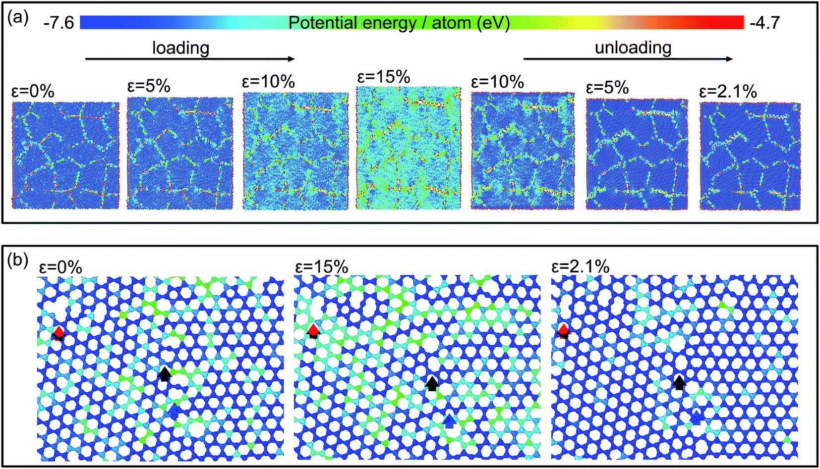 | ||
| Fig. 3 (a) Snapshots of the atomic configurations in a loading–unloading cycle; (b) structural evolution in local regions during the loading and unloading processes. | ||
Bond breaking and reforming in GBs are sensitive to the temperature and strain rate in mechanical loading.43 Therefore, the energy dissipation coefficient should also be temperature and strain rate dependent. Taking the graphene sheets with grains in the sizes of 2.2 nm, 4.0 nm and 6.6 nm as examples, two sets of MD simulations are performed: (1) in the temperature range of 10–1500 K but at a given strain rate of 108 s−1 and (2) in the strain rate range of 108 to 1010 s−1 but at a given temperature of 300 K. Fig. 4(a) and (b) show the energy dissipation coefficients as a function of temperature and strain rate, respectively. As shown in Fig. 4(a), the energy dissipation coefficients increase with temperature almost linearly, for example, from 0.075 at 10 K to 0.38 at 1500 K by 407% for the graphene sheet with 4.0 nm grains. Kinetically, the atoms in the GBs oscillate more at higher temperature. The energy barrier can be overcome more easily to promote bond breaking, rotation, and reforming in the GBs in addition to the formation of polygonal holes44 and buckling along the GBs.45 As shown in Fig. 4(b), the energy dissipation coefficients decrease with increasing strain rate slightly. At lower strain rate, the atoms in the GBs have enough time to rearrange during tensile loading and the irreversible structural evolution is more substantial thereby leading to a larger energy dissipation coefficient.44 However, the dependence on the strain rate is not appreciable. Furthermore, the graphene sheets with smaller grains have larger grain boundary densities [Fig. 1(a)] and irreversible bond rearrangement is more likely in the GBs. Hence, the energy dissipation coefficient becomes more sensitive to the temperature and strain rate in the graphene sheets with smaller grains.
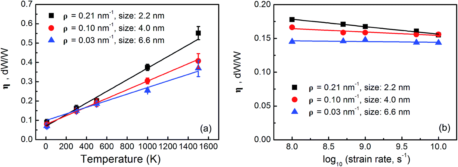 | ||
| Fig. 4 (a) Energy dissipation coefficients of nanocrystalline graphene sheets at different temperature; (b) logarithmic plots of the energy dissipation coefficients a function of strain rate. | ||
Large strain usually leads to more structural rearrangement in the GBs and hence, energy dissipation is more substantial. Unloading from different strain values is simulated in the temperature range of 10–1500 K. Fig. 5(a) shows the simulated stress–strain curves of graphene sheets with a grain size of 4.0 nm at 300 K. Elastic lattice distortion dominates at small strain, but bond rearrangement in the GBs becomes more significant with increasing strain. Consequently, the residual strain increases from 0.23% to 2.1% and the enclosed area by the loading and unloading stress–strain curves is substantially enlarged. The strain from where the graphene sheets are unloaded increases from 5% to 15% and the energy dissipation coefficients increase with the maximum unloading strain, particularly at a high temperature [Fig. 5(b)]. For example, the energy dissipation coefficient at 300 K increases by 62.8% when the maximum unloading strain increases from 5% to 15%, whereas it increases by 115% at 1500 K. Tight-binding MD simulation indicates that evaporation of carbon dimers and sequential Stone–Wales transformation of carbon bonds lead to rapid motion and annihilation of the GBs particularly those with large carbon rings.46 The larger energy dissipation coefficient can be attributed to enhanced reconstruction of the local atomic configuration in the GBs.
 | ||
| Fig. 5 (a) The loading stress–strain curves and those unloaded from different maximum strains; (b) energy dissipation coefficient at different temperatures. | ||
4. Conclusion
In summary, MD simulation is conducted to study the deformation behavior of nanocrystalline graphene sheets. Different from single-crystal graphene sheets, the loading and unloading stress–strain curves do not coincide with each other and nonzero residual strain is usually observed despite unloading from a strain much smaller than fracture strain. It indicates energy dissipation and irreversible structural changes. The mechanical work W in the loading process is converted into elastic strain energy in the lattice and chemical energy in the GBs and the elastic strain energy in the lattice is released in the unloading process, but the chemical energy due to bond breaking and reforming in the GBs cannot be released. The energy dissipation increases with reducing grain size, especially at a high temperature, and the deformation reversibility of nanocrystalline graphene deteriorates consequently. Our results offer a potential guidance for NEMS design and development.Acknowledgements
This work was jointly supported by National Natural Science Foundation of China (Grant No. 51271139, 51471130, 51302162), Fundamental Research Funds for the Central Universities, and City University of Hong Kong Applied Research Grant (ARG) No. 9667104.References
- K. S. Novoselov, A. K. Geim, S. V. Morozov, D. Jiang, Y. Zhang, S. V. Dubonos, I. V. Grigorieva and A. A. Firsov, Science, 2004, 306, 666–669 CrossRef CAS PubMed.
- C. Lee, X. Wei, J. W. Kysar and J. Hone, Science, 2008, 321, 385–388 CrossRef CAS PubMed.
- K. I. Bolotin, K. Sikes, Z. Jiang, M. Klima, G. Fudenberg, J. Hone, P. Kim and H. Stormer, Solid State Commun., 2008, 146, 351–355 CrossRef CAS.
- F. Pellegrino, G. Angilella and R. Pucci, High Pressure Res., 2012, 32, 18–22 CrossRef CAS.
- C. Jin, H. Lan, L. Peng, K. Suenaga and S. Iijima, Phys. Rev. Lett., 2009, 102, 205501 CrossRef PubMed.
- Z. Jing, Z. G. Yu and S. D. Xia, Chin. Phys. B, 2013, 22, 057701 CrossRef.
- N. Levy, S. Burke, K. Meaker, M. Panlasigui, A. Zettl, F. Guinea, A. C. Neto and M. Crommie, Science, 2010, 329, 544–547 CrossRef CAS PubMed.
- S. Stankovich, D. A. Dikin, G. H. Dommett, K. M. Kohlhaas, E. J. Zimney, E. A. Stach, R. D. Piner, S. T. Nguyen and R. S. Ruoff, Nature, 2006, 442, 282–286 CrossRef CAS PubMed.
- S. H. Bae, Y. Lee, B. K. Sharma, H. J. Lee, J. H. Kim and J. H. Ahn, Carbon, 2013, 51, 236–242 CrossRef CAS.
- K. Y. Shin, J. Y. Hong and J. Jang, Chem. Commun., 2011, 47, 8527–8529 RSC.
- T. Ramanathan, A. Abdala, S. Stankovich, D. Dikin, M. Herrera-Alonso, R. Piner, D. Adamson, H. Schniepp, X. Chen and R. Ruoff, Nat. Nanotechnol., 2008, 3, 327–331 CrossRef CAS PubMed.
- F. Banhart, J. Kotakoski and A. V. Krasheninnikov, ACS Nano, 2010, 5, 26–41 CrossRef PubMed.
- J. H. Chen, W. Cullen, C. Jang, M. Fuhrer and E. Williams, Phys. Rev. Lett., 2009, 102, 236805 CrossRef PubMed.
- B. Huang, M. Liu, N. Su, J. Wu, W. Duan, B. L. Gu and F. Liu, Phys. Rev. Lett., 2009, 102, 166404 CrossRef PubMed.
- J. Dai, J. Yuan and P. Giannozzi, Appl. Phys. Lett., 2009, 95, 232105 CrossRef.
- S. Malola, H. Hakkinen and P. Koskinen, Phys. Rev. B: Condens. Matter Mater. Phys., 2010, 81, 165447 CrossRef.
- O. V. Yazyev and S. G. Louie, Phys. Rev. B: Condens. Matter Mater. Phys., 2010, 81, 195420 CrossRef.
- A. J. Cao and Y. T. Yuan, Appl. Phys. Lett., 2012, 100, 211912 CrossRef.
- G. H. Lee, R. C. Cooper, S. J. An, S. Lee, A. van der Zande, N. Petrone, A. G. Hammerherg, C. Lee, B. Crawford, W. Oliver, J. W. Kysar and J. Hone, Science, 2013, 340, 1073–1076 CrossRef CAS PubMed.
- Z. Yang, Y. Huang, F. Ma, Y. Sun, K. Xu and P. K. Chu, Mater. Sci. Eng., B, 2015, 198, 95–101 CrossRef CAS.
- T. H. Liu, G. Gajewski, C. W. Pao and C. C. Chang, Carbon, 2011, 49, 2306–2317 CrossRef CAS.
- J. T. Wu and Y. J. Wei, J. Mech. Phys. Solids, 2013, 61, 1421–1432 CrossRef CAS.
- T. H. Liu, C. W. Pao and C. C. Chang, Carbon, 2012, 50, 3465–3472 CrossRef CAS.
- R. Grantab, V. B. Shenoy and R. S. Ruoff, Science, 2010, 330, 946–948 CrossRef CAS PubMed.
- H. I. Rasool, C. Ophus, W. S. Klug, A. Zettl and J. K. Gimzewski, Nat. Commun., 2013, 4, 2811 Search PubMed.
- H. Y. Cao, H. Xiang and X. G. Gong, Solid State Commun., 2012, 152, 1807–1810 CrossRef CAS.
- A. Bagri, S. P. Kim, R. S. Ruoff and V. B. Shenoy, Nano Lett., 2011, 11, 3917–3921 CrossRef CAS PubMed.
- B. Wang, Y. Puzyrev and S. T. Pantelides, Carbon, 2011, 49, 3983–3988 CrossRef CAS.
- J. Kotakoski and J. C. Meyer, Phys. Rev. B: Condens. Matter Mater. Phys., 2012, 85, 195447 CrossRef.
- A. Cao and J. Qu, Appl. Phys. Lett., 2013, 102, 071902 CrossRef.
- D. W. Brenner, O. A. Shenderova, J. A. Harrison, S. J. Stuart, B. Ni and S. B. Sinnott, J. Phys.: Condens. Matter, 2002, 14, 783 CrossRef CAS.
- O. A. Shenderova, D. W. Brenner, A. Omeltchenko, X. Su and L. H. Yang, Phys. Rev. B: Condens. Matter Mater. Phys., 2000, 61, 3877–3888 CrossRef CAS.
- W. G. Hoover, Phys. Rev. A, 1985, 31, 1695 CrossRef.
- H. Zhao, K. Min and N. Aluru, Nano Lett., 2009, 9, 3012–3015 CrossRef CAS PubMed.
- A. Hadizadeh Kheirkhah, E. Saeivar Iranizad, M. Raeisi and A. Rajabpour, Solid State Commun., 2014, 177, 98–102 CrossRef CAS.
- N. N. Li, Z. D. Sha, Q. X. Pei and Y. W. Zhang, J. Phys. Chem. C, 2014, 118, 13769–13774 CrossRef CAS.
- S. Pathak, E. J. Lim, P. Pour Shahid Saeed Abadi, S. Graham, B. A. Cola and J. R. Greer, ACS Nano, 2012, 6, 2189–2197 CrossRef CAS PubMed.
- R. W. Balluffi, S. M. Allen and W. C. Carter, Kinet. Mater., 2005, 253–283 Search PubMed.
- P. J. van der Zaag, P. J. van der Valk and M. T. Rekveldt, Appl. Phys. Lett., 1996, 69, 2927–2929 CrossRef CAS.
- I. Jackson, J. D. Fitz Gerald, U. H. Faul and B. H. Tan, J. Geophys. Res.: Solid Earth, 2002, 107, 423 Search PubMed.
- H. Padilla II, C. Smith, J. Lambros, A. Beaudoin and I. Robertson, Metall. Mater. Trans. A, 2007, 38, 2916–2927 CrossRef.
- G. Cannelli, R. Cantelli, F. Cordero, G. Costa, M. Ferretti and G. Olcese, Europhys. Lett., 1988, 6, 271 CrossRef CAS.
- L. Yi, Z. Yin, Y. Zhang and T. Chang, Carbon, 2013, 51, 373–380 CrossRef CAS.
- M. Li, Z. Kang, R. Li, X. H. Meng and Y. J. Lu, J. Phys. D: Appl. Phys., 2013, 46, 1274 Search PubMed.
- J. F. Zhang, J. J. Zhao and J. P. Lu, ACS Nano, 2012, 6, 2704–2711 CrossRef CAS PubMed.
- G. D. Lee, E. Yoon, C. Z. Wang and K. M. Ho, J. Phys.: Condens. Matter, 2013, 25, 155301 CrossRef PubMed.
| This journal is © The Royal Society of Chemistry 2016 |