Molecular dynamics simulation studies on the plastic behaviors of an iron nanowire under torsion
Chong Qiaoa,
Yanli Zhoub,
Xiaolin Caiac,
Weiyang Yuac,
Bingjie Dua,
Haiyan Wanga,
Songyou Wangde and
Yu Jia*a
aInternational Laboratory for Quantum Functional Materials of Henan, School of Physics and Engineering, Zhengzhou University, Zhengzhou 450001, China. E-mail: jiayu@zzu.edu.cn
bDepartment of Mechanical and Electrical Engineering, Henan Industry and Trade Vocational College, Zhengzhou 451191, China
cSchool of Physics and Chemistry, Henan Polytechnic University, Jiaozuo 454000, China
dShanghai Ultra-Precision Optical Manufacturing Engineering Center, Department of Optical Science and Engineering, Fudan University, Shanghai, 200433, China
eKey Laboratory for Information Science of Electromagnetic Waves (MoE), Shanghai 200433, China
First published on 14th March 2016
Abstract
The plastic deformation mechanism of iron (Fe) nanowires under torsion is studied using the molecular dynamics (MD) method by applying an external driving force at a constant torsion speed. We find that the deformation behavior depends on the orientation of the wire. The dislocations in 〈100〉 and 〈111〉 oriented nanowires propagate through the nanowires under torsion, whereas those in 〈110〉 oriented nanowires divide the wire into two parts. The situation that there is a low angle twist grain boundary (GB) in the nanowires is also under consideration. The results reveal that the dislocations are concentrated on the GB in the initial state, presenting different patterns of dislocation network. The networks change depending on the twist direction. They shrink with increase in twist angle but expand with the decreasing twist angle, presenting an asymmetric phenomenon. Our findings can help us more thoroughly understand the plastic deformation mechanism of Fe nanowires under torsion.
1. Introduction
Nanowires are attracting a lot of interest due to their unique properties and potential as fundamental building blocks of nanotechnology, having been envisioned to be applied in miniaturized electrical, optical, magnetic, catalytic and mechanical systems.1–6 Therefore, in order to build more robust nanodevices, it is necessary to study the mechanical behaviors of their fundamental deformation. However, it is difficult and challenging to perform experiments to evaluate the mechanical properties of nanowires at nanoscale. With the rapid improvement of computational capability, MD simulation, as an efficient tool to study the mechanical behaviors of nanomaterials, has been used widely.For tensile properties of nanowires, Wu et al.7 performed simulations on the failure of copper nanowire, and they confirmed that nanowire failure depends on the length of nanowire. The plastic deformation mechanism of Cu nanowires was investigated by Xie et al.8 using the MD method. They pointed out a new mechanism of face centered cubic (fcc)–body centered cubic (bcc)–hexagonal close packed (hcp) phase transformation at a high strain rate. Tensile testing of Fe and FeCr nanowires was done by Byggmastar et al.9 using MD simulations. And they identified that the pure Fe nanowires are elastically softer than bulk Fe. Other simulations made by Sainath et al.10–12 studied the tensile deformation and fracture behaviors of Fe nanowires, and the results revealed that the deformation behaviors depend on not only the size but also the orientation. Healy et al.13 found the compression-tension asymmetry in plasticity of Fe nanopillars by MD simulation. For torsion properties of nanowires, simulations were carried out by Christopher et al.14,15 to research the plasticity of metal nanowires under torsion. It was observed that the plastic deformation of nanowires under torsion could be either homogeneous or heterogeneous, regardless of size, depending on the wire orientation, and the plasticity is dominated by dislocation nucleation from free surfaces. Gao et al.16 made simulation to investigate the mechanical behaviors of Cu nanowire under torsion, and they discovered that the nanowires take different paths of deformation at different loading rates. We recently also discussed the evolution behaviors of GB for metals and their bimetal interface under torsion. Our finding shows that bimetal interface has an inhibition on the evolution of GB.17 The simulations discussed above reveal that MD method is a good tool to study the mechanical behaviors of nanomaterials.
Bcc Fe nanowires present good magnetic properties. Therefore, they are suitable to apply in data-storage media and memory devices, spin electronics, medical sensors and as an enhancement agent for magnetic resonance imaging.18–20 But studies on Fe nanowires are not perfect or sufficient. Now the work is confined to the study of plastic deformation of Fe nanowire under tension and compression. As for torsion effects, the very common phenomena in micromechanical application of nanodevices, such as molecular motors, nano gears and nano bearings, as far as we know, have not been studied in Fe nanowires before. However, it is inevitable to keep some defects in the nanowires under some conditions, such as GB, having a great influence on the mechanical properties of the nanowires.
In this work, we investigate the plastic deformation behaviors of Fe nanowires in three orientations under torsion using the MD method, together with the evolution phenomena of their low angle twist GBs. Dislocation structures are presented with the time to show the deformation mechanism. And the potential energies of the nanowires as a function of time are also depicted to explain the plastic deformation behaviors. They can help us understand the deformation behaviors of Fe nanowires easily. And it is convenient for us to design the nanodevices made of Fe nanowires.
2. Methods
The simulations have been carried out using a parallel program, LAMMPS, which is widely used in MD simulations,21–24 developed by Plimpton.25 Empirical inter-atomic potential developed by Mendelev et al.26 with an embedded-atom method was employed. It coincides with the experiment results very well. As far as we are concerned, it has been used to study the motion of dislocation for Fe in MD simulations widely.10-12,27,28 The simulation model was a cylindrical nanowire with a length of 15 nm and a radius of 5 nm, in total comprising 100![[thin space (1/6-em)]](https://www.rsc.org/images/entities/char_2009.gif) 590,
590,![[thin space (1/6-em)]](https://www.rsc.org/images/entities/char_2009.gif) 101
101![[thin space (1/6-em)]](https://www.rsc.org/images/entities/char_2009.gif) 288 and 100
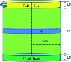
288 and 100![[thin space (1/6-em)]](https://www.rsc.org/images/entities/char_2009.gif) 828 atoms in 〈100〉, 〈110〉 and 〈111〉 orientations, respectively. When there was a twist GB, the nanowires was divided into two equal parts by the GB. The initial twist angle was set to 9.8 degrees. To do this, we can rotate the upper part with an anticlockwise angle of 9.8 degrees. Then it was treated as the initial twist angle of the model. The structures of GB were obtained by the following steps. Firstly, the initial distance of two grains was set to larger than the interlayer spacing of adjacent planes. Then an energy minimization of the system was performed by conjugate gradient algorithm to obtain a stable structure. We applied periodic boundary conditions in the axial direction with free boundary conditions in the other two directions. There are about 1.5 nm atoms layers above (or below) the bottom (or top) layers were fixed as rigid layers, and a twist rate of 2π × 10−3 rad fs−1 was applied on the top rigid layers, as shown in Fig. 1. We have also tested our simulation results by applying different rates, and it shows that there is little influence on the simulation results with the rotation rate from 0.1π × 10−3 rad fs−1 to 10π × 10−3 rad fs−1. The canonical ensemble was applied throughout the whole MD simulations with a Nose–Hoover thermostat and the time step was set to be 1 fs. In order to avoid the effect of temperature on the dislocation nucleation in the sliding process, the system was thermally equilibrated to a low temperature of 50 K. The centro-symmetry (CS) parameter29 for each atom in the model, except the rigid layers, was calculated to clearly visualize the various defects. For Fe, we have tested the CS parameters in different configurations. Here we use CS ≥ 0.8 which is enough to show all kinds of crystal defects. All the figures in this work were coloured based on atoms' CS values. To study the temperature effect on the system in the simulations, the cases at 20 K and 100 K are taken into consideration, respectively. As for size effect, the models with lengths of 12 nm and 20 nm, and the models with radii of 3 nm and 7 nm are also taken into consideration, respectively.
828 atoms in 〈100〉, 〈110〉 and 〈111〉 orientations, respectively. When there was a twist GB, the nanowires was divided into two equal parts by the GB. The initial twist angle was set to 9.8 degrees. To do this, we can rotate the upper part with an anticlockwise angle of 9.8 degrees. Then it was treated as the initial twist angle of the model. The structures of GB were obtained by the following steps. Firstly, the initial distance of two grains was set to larger than the interlayer spacing of adjacent planes. Then an energy minimization of the system was performed by conjugate gradient algorithm to obtain a stable structure. We applied periodic boundary conditions in the axial direction with free boundary conditions in the other two directions. There are about 1.5 nm atoms layers above (or below) the bottom (or top) layers were fixed as rigid layers, and a twist rate of 2π × 10−3 rad fs−1 was applied on the top rigid layers, as shown in Fig. 1. We have also tested our simulation results by applying different rates, and it shows that there is little influence on the simulation results with the rotation rate from 0.1π × 10−3 rad fs−1 to 10π × 10−3 rad fs−1. The canonical ensemble was applied throughout the whole MD simulations with a Nose–Hoover thermostat and the time step was set to be 1 fs. In order to avoid the effect of temperature on the dislocation nucleation in the sliding process, the system was thermally equilibrated to a low temperature of 50 K. The centro-symmetry (CS) parameter29 for each atom in the model, except the rigid layers, was calculated to clearly visualize the various defects. For Fe, we have tested the CS parameters in different configurations. Here we use CS ≥ 0.8 which is enough to show all kinds of crystal defects. All the figures in this work were coloured based on atoms' CS values. To study the temperature effect on the system in the simulations, the cases at 20 K and 100 K are taken into consideration, respectively. As for size effect, the models with lengths of 12 nm and 20 nm, and the models with radii of 3 nm and 7 nm are also taken into consideration, respectively.
3. Results and discussions
3.1 The deformation behavior of defect-free nanowire under torsion
Fig. 2(a0) is the initial configuration in 〈100〉 oriented nanowire. Fig. 2(a1) and (a2) are the defect structures of Fig. 2(a0) after 62 ps and 80 ps, respectively. Fig. 2(a3) and (a4) are their side views, respectively. Fig. 2(a0) reveals that there is no dislocation in the initial nanowire except the boundary shown in a circle. With an increasing of the twist angle, the nanowire undergoes elastic deformation first, and then the plastic deformation. In the stage of elastic deformation, without torsion, the deformation disappears gradually, so the wire can change back to its initial configuration. Beyond the elastic limit, dislocations begin to generate on the nanowire surface, and then propagate within the nanowire, finally form a dislocation line with a mirrored “C” shape which is marked with a red curve, as seen in Fig. 2(a3). With the plastic deformation continue, the screw dislocation line extends through the nanowire from the driving end to the fixed end. In addition, more dislocation lines begin to generate from the boundary, and they intersect each other eventually, as shown in Fig. 2(a4), forming a three-dimensional network structure which can prevent the slippage of dislocations. Therefore, the strength of nanowire in 〈100〉 orientation can be enhanced. It is manifested that dislocations in 〈100〉 oriented nanowire are inclined to propagate along the 〈100〉 orientation, and a modest twist may improve the strength of 〈100〉 oriented Fe nanowire.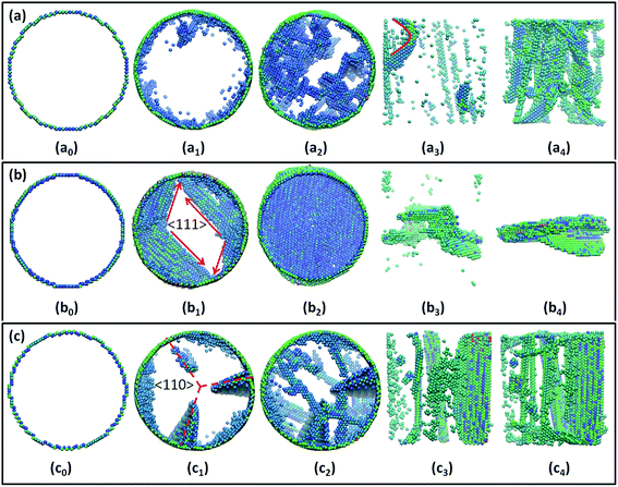 | ||
| Fig. 2 (a), (b) and (c) are the dislocation evolution configurations of Fe nanowires in 〈100〉, 〈110〉 and 〈111〉 orientations, respectively. | ||
Different from the case above, the plastic deformation behaviors of 〈110〉 oriented nanowire presents an intriguing phenomenon, as illustrated in Fig. 2(b). Fig. 2(b0) is the initial configuration. Fig. 2(b1) and (b2) are the defect structures of Fig. 2(b0) after 60 ps and 80 ps, respectively. Fig. 2(b3) and (b4) are their side views, respectively. At the beginning of the deformation, dislocation planes are generated on the nanowire surface gradually, and then propagate to the center of the wire with the increasing twist angle, as seen in Fig. 2(b1) and (b3). The red arrows marked in Fig. 2(b1) represent the Burgers vectors which are parallel to the 〈111〉 orientation. As the twisting continues, the propagation directions of dislocations normal to the Burgers vectors move to the center of the wire. And eventually a larger dislocation plane is formed, namely the GB, dividing the whole wire into two parts, as depicted in Fig. 2(b2) and (b4), respectively. This phenomenon coincides with the theory28,30 that the 〈111〉 orientation is the slip direction of (110) slip plane in Fe nanowire.
Fig. 2(c0) is the initial configuration of 〈111〉 oriented nanowire. Fig. 2(c1) and (c2) depict the dislocation structures of Fig. 2(c0) after 60 and 80 ps, respectively. Fig. 2(c3) and (c4) are their side views, respectively. It reveals that the deformation behavior shows a similar phenomenon to the case of 〈100〉 oriented wire. The nanowire boundary begins to produce dislocations with increase in twist angle, and then the dislocations form a dislocation line finally. However, there are still some differences, the nanowire surface also produces slip planes extending through the wire, as depicted in Fig. 2(c1) and (c3), respectively. The three dot lines marked in Fig. 2(c1) represent the propagation directions of the dislocations. Each two lines make an angle of 120° which is in agreement with the 〈110〉 crystal orientation family. Moreover, when the twist is over a certain degree, dislocations normal to the rotation axial are generated at two ends of the wire with the increasing twist angle, as shown in Fig. 2(c2) and (c4), respectively.
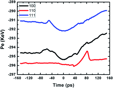
Fig. 3 illustrates the potential energies of the three oriented nanowires change with time. Although the nanowires have different orientations, they have the same trends. From beginning to the 56 ps, the nanowires are in the elastic stage under external stress, so the curves increase in a quadratic form with time. In the vicinity of 60 ps, they reach the first yield point, the energy curves decrease sharply because of the dislocation. After this, the curves begin to increase linearly. As for the curve in 〈111〉 oriented nanowires, there is a fluctuation in the vicinity of yield point. This may be that the wire generates some slide planes which may decrease the energy absorbed by dislocation atoms. Compared the three curves, it can be seen that the 〈100〉 oriented nanowires undergoes a longer elastic stage, therefore, the elasticity of Fe nanowires in 〈100〉 orientation is better than those in the other orientations.
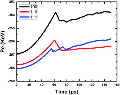 | ||
| Fig. 3 Black, red and blue curves represent the potential energy of the region between the two ends in the 〈100〉, 〈110〉 and 〈111〉 oriented nanowires, respectively. | ||
3.2 The deformation behavior of nanowire with a twist GB under torsion
The twist GB evolution behaviors of nanowires in three orientations under anticlockwise and clockwise torsion are presented in Fig. 4(a), (b) and (c), respectively. The initial twist GB structures of different orientations display different patterns of planar networks which have been reported31,32 in other materials. Fig. 4(a0) is the top view of the initial GB structure in 〈100〉 oriented nanowire, forming a rectangular dislocation network with uniformly distributed orthogonal dislocation lines. A similar phenomenon has been researched by Hafez Haghighat et al.33 Fig. 4(a1), (a2) and (a3), (a4) are the anticlockwise and clockwise twist GB configurations of the initial GB structure after 20 ps and 40 ps, respectively. The dislocation lines are close to each other gradually under anticlockwise torsion with the increasing twist angle, leading to a shrinking of the dislocation network as shown in Fig. 4(a1) and (a2), respectively. This phenomenon is in good agreement with our previous report17 for face-centered cubic metals before. On the other hand, the screw dislocation lines are far away from each other under clockwise torsion with the twist angle becoming smaller, as seen in Fig. 4(a3). As the twisting continues, the screw dislocation lines adjacent to the boundary become curved and irregular, as presented in Fig. 4(a4), which may be the effect of the boundary.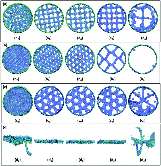 | ||
| Fig. 4 (a), (b) and (c) are the GB evolution behaviors of Fe nanowires in 〈100〉, 〈110〉 and 〈111〉 orientations, respectively. (d) is the side view of (c) for reference. | ||
The top view of initial twist GB structure in 〈110〉 oriented nanowire can be seen in Fig. 4(b0). Fig. 4(b1), (b2) and (b3), (b4) are the anticlockwise and clockwise twist GB configurations of the initial GB structure after 20 ps and 40 ps, respectively. The dislocation network consists of zigzag dislocation lines forming many junctions of an “X” shape which can be seen in Fig. 4(b0) with a red circle. Each junction consists of four screw dislocations. Under anticlockwise torsion, with the twist angle becoming larger, the dislocation lines tend to move to the center of the GB, so the “X” junction shrinks leading to a shrinking of the dislocation network, as shown in Fig. 4(b1) and (b2), respectively. Therefore, the density of dislocation increases gradually. However, the dislocation lines propagate to the border of GB under clockwise torsion. The “X” junction expands with the increasing twist angle, resulting in a decrease of dislocation density, as revealed in Fig. 4(b3). As the twisting continues, the dislocations are almost lost in the twist GB finally, as depicted in Fig. 4(b4). The two parts have a trend to form a defect-free nanowire. It is revealed that rotation provides a feasible method to eliminate the dislocations in twist GB for 〈110〉 oriented nanowires, which can improve the mechanical properties of the nanomaterials.
Fig. 4(c0) depicts the top view of the initial twist GB structure in 〈111〉 oriented nanowire. Fig. 4(c1), (c2) and (c3), (c4) are the anticlockwise and clockwise twist GB configurations of Fig. 4(c0) after 20 ps and 60 ps, respectively. The screw dislocation network is different from the cases having been discussed above, consisting of three group of parallel dislocation lines. The dislocation lines immigrate to the center of GB under anticlockwise torsion. The parallel dislocation lines are close to each other leading to a shrinking of the dislocation network as shown in Fig. 4(c1) and (c2), respectively. Then the density of the dislocations increases with increase in twist angle. Under clockwise torsion, with the twist angle decreasing, the parallel dislocation lines are far away from each other gradually resulting in an expansion of the dislocation network, as presented in Fig. 4(c3) and (c4), respectively. Fig. 4(d) is the side view of the 〈111〉 oriented wire corresponding to Fig. 4(c). It illustrates the dislocations can move to the grain interior eventually, which coincides with the dislocation evolution tendency of defect-free nanowires.
From Fig. 5 the potential energy curves of 〈100〉 and 〈111〉 oriented nanowires increase under clockwise torsion, whereas they increase first and then tend to equilibrium under anticlockwise torsion. This is because the rotation of the specimen is inhibited with the reducing dislocations under clockwise torsion then the potential energy starts to be stored in the nanowires. Under anticlockwise torsion, the dislocations increase first, and then form a steady slip layer making the rotation happen easily, so the potential energy becomes to equilibrium finally. As for the 〈110〉 oriented nanowires, the curve is similar to other orientations under anticlockwise torsion. However, it drops first and then presents a similar phenomenon to the defect-free nanowires under clockwise torsion. This is because the dislocations disappear gradually with the decreasing twist angle, and then the model undergoes an elastic deformation and a plastic deformation successively with increase in twist angle.
Comparing the twist GB evolution behaviors of the three oriented nanowires studied above. It is concluded that the dislocation networks shrink under anticlockwise torsion but expand under clockwise torsion showing an asymmetric phenomenon. Therefore, the density of dislocation increases with the increasing twist angle but decreases with the decreasing twist angle. This may be that the misfit lattice sites increase when the twist angle becomes larger but decrease when the angle becomes smaller. In addition, the patterns of the dislocation networks are also different from each other, just depending on the orientation of the nanowires. The dislocation network in 〈100〉 oriented nanowire consists of two group of parallel screw dislocation lines. While the dislocation network in 〈111〉 oriented nanowire is made of three groups of parallel dislocation lines. As for the dislocation network in 〈110〉 oriented nanowire, it shows an intriguing pattern, forming many junctions of an “X” shape.
Now we give an interpretation of the GB evolution behaviors we have studied above. The twist GB structure in 〈100〉 oriented nanowires can be seen in Fig. 6(a). Crystal orientations, i.e. [010], [001], [0![[1 with combining macron]](https://www.rsc.org/images/entities/char_0031_0304.gif) 0] and [00
0] and [00![[1 with combining macron]](https://www.rsc.org/images/entities/char_0031_0304.gif) ], are marked with red arrows to describe the dislocation slip directions. They are parallel to the dislocation lines and form an orthogonal structure which is in agreement with the dislocation network. That is to say, the 〈110〉 crystal orientation family are the slip directions of twist GB in (100) plane. This may be that atomic arrangement in 〈100〉 directions is relative loose, the interaction between atoms is weaker than the cases in 〈110〉 and 〈111〉 directions making atoms glide easily in these directions. For screw dislocation, the propagation directions of dislocation lines are perpendicular to the dislocation lines. Under anticlockwise torsion, the immigration directions of dislocation lines point to the center of GB resulting in the dislocation lines close to each other. Whereas they propagate to the border of GB, leading to an expansion of the dislocation network under clockwise torsion.
], are marked with red arrows to describe the dislocation slip directions. They are parallel to the dislocation lines and form an orthogonal structure which is in agreement with the dislocation network. That is to say, the 〈110〉 crystal orientation family are the slip directions of twist GB in (100) plane. This may be that atomic arrangement in 〈100〉 directions is relative loose, the interaction between atoms is weaker than the cases in 〈110〉 and 〈111〉 directions making atoms glide easily in these directions. For screw dislocation, the propagation directions of dislocation lines are perpendicular to the dislocation lines. Under anticlockwise torsion, the immigration directions of dislocation lines point to the center of GB resulting in the dislocation lines close to each other. Whereas they propagate to the border of GB, leading to an expansion of the dislocation network under clockwise torsion.
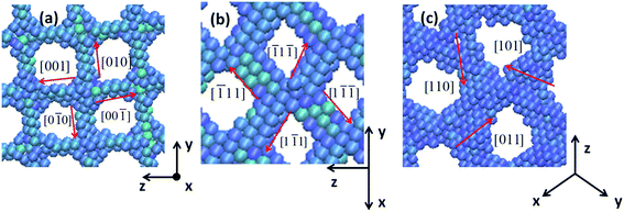 | ||
| Fig. 6 (a), (b) and (c) are the local structures of Fig. 4(a0), (b0) and (c0), respectively. The red arrows represent the dislocation slip directions. | ||
Fig. 6(b) presents the local structure of twist GB in 〈110〉 orientation, showing an “X” shape. Crystal orientations, i.e. [![[1 with combining macron]](https://www.rsc.org/images/entities/char_0031_0304.gif) 1
1![[1 with combining macron]](https://www.rsc.org/images/entities/char_0031_0304.gif) ], [
], [![[1 with combining macron]](https://www.rsc.org/images/entities/char_0031_0304.gif) 11], [1
11], [1![[1 with combining macron]](https://www.rsc.org/images/entities/char_0031_0304.gif) 1] and [1
1] and [1![[1 with combining macron]](https://www.rsc.org/images/entities/char_0031_0304.gif)
![[1 with combining macron]](https://www.rsc.org/images/entities/char_0031_0304.gif) ], are noted with red arrows to represent the dislocation slip directions. They are parallel to the dislocation lines, forming an “X” junction. The high angle between two atom arrangement directions (between [
], are noted with red arrows to represent the dislocation slip directions. They are parallel to the dislocation lines, forming an “X” junction. The high angle between two atom arrangement directions (between [![[1 with combining macron]](https://www.rsc.org/images/entities/char_0031_0304.gif) 11] and [1
11] and [1![[1 with combining macron]](https://www.rsc.org/images/entities/char_0031_0304.gif) 1], [1
1], [1![[1 with combining macron]](https://www.rsc.org/images/entities/char_0031_0304.gif)
![[1 with combining macron]](https://www.rsc.org/images/entities/char_0031_0304.gif) ] and [
] and [![[1 with combining macron]](https://www.rsc.org/images/entities/char_0031_0304.gif) 1
1![[1 with combining macron]](https://www.rsc.org/images/entities/char_0031_0304.gif) ]) is measured to be 109.5°, which coincides with the theory value. Then it is manifested that the slip directions of (110) twist GB are 〈111〉 crystal orientation family. The driving forces of the four directions are equal in size, because they are symmetrical. Under anticlockwise torsion, the propagation directions of the dislocation are normal to the dislocation lines and point to the area of low angles (between [
]) is measured to be 109.5°, which coincides with the theory value. Then it is manifested that the slip directions of (110) twist GB are 〈111〉 crystal orientation family. The driving forces of the four directions are equal in size, because they are symmetrical. Under anticlockwise torsion, the propagation directions of the dislocation are normal to the dislocation lines and point to the area of low angles (between [![[1 with combining macron]](https://www.rsc.org/images/entities/char_0031_0304.gif) 11] and [
11] and [![[1 with combining macron]](https://www.rsc.org/images/entities/char_0031_0304.gif) 1
1![[1 with combining macron]](https://www.rsc.org/images/entities/char_0031_0304.gif) ], [1
], [1![[1 with combining macron]](https://www.rsc.org/images/entities/char_0031_0304.gif) 1] and [1
1] and [1![[1 with combining macron]](https://www.rsc.org/images/entities/char_0031_0304.gif)
![[1 with combining macron]](https://www.rsc.org/images/entities/char_0031_0304.gif) ]). The four Burgers vectors interact with each other resulting in a shrinking of the dislocation network. While the propagation directions of dislocation lines point to the area of high angles under clockwise torsion. The dislocation lines expand to make an “X” junction become larger.
]). The four Burgers vectors interact with each other resulting in a shrinking of the dislocation network. While the propagation directions of dislocation lines point to the area of high angles under clockwise torsion. The dislocation lines expand to make an “X” junction become larger.
The dislocation structure in (111) twist GB is consist of three groups of parallel dislocation lines. Therefore, there are three slip directions in the local structure as shown in Fig. 6(c). Crystal orientations, i.e. [011], [101] and [110], are marked with red arrows to represent the dislocation slip direction which is consistent with the atom rearrangement direction. Then we can know that 〈110〉 crystal orientation family are the dislocation slip directions of (111) twist GB. Under anticlockwise torsion, the propagation directions of dislocation lines are perpendicular to the dislocation lines and point to the center of GB, leading to a shrinking of the dislocation network. Under clockwise torsion, the dislocation lines point to the border of GB resulting in an expansion of dislocation structure.
3.3 The temperature effect on deformation behavior of nanowire under torsion
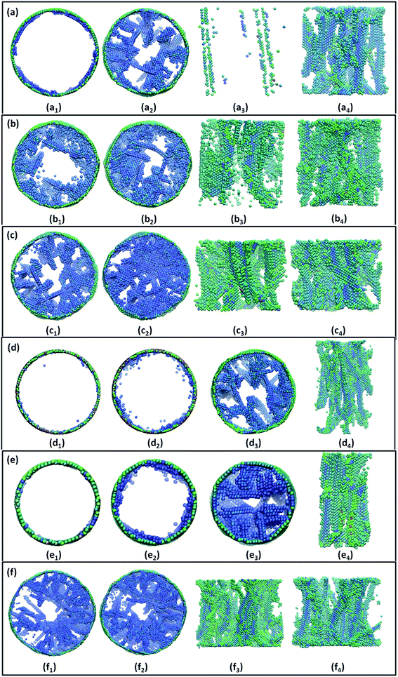
Now we take temperature effect into consideration. The initial dislocation configurations are not shown because there is no dislocation in defect-free nanowires without torsion. Fig. 7(a) and (b) are the dislocation structures of the model at 20 K and 100 K, respectively. Fig. 7(a1) and (a2) are the dislocation structures of initial configuration after 62 ps and 80 ps, respectively. Fig. 7(a3) and (a4) are their side views, respectively. Fig. 7(b) shows the dislocation structures of the model corresponding to Fig. 7(a) at the same time. At 62 ps, there is no dislocation line in Fig. 7(a1), whereas there are many dislocation lines in Fig. 7(b1). At 80 ps, all of them form three-dimensional network structures, as shown in Fig. 7(a4) and (b4), respectively. Then it can be seen that the evolution speed increases with the rising temperature, but temperature does not change the evolution tendency. This may be that high temperature can improve the activity of atoms. As for the nanowire with a twist GB, temperature also has nothing with the deformation trend of dislocation.3.4 The size effect on deformation behavior of nanowire under torsion
As for size effect, both length and radius are taken into consideration. Fig. 7(c) and (d) are the dislocation structures of the model with a length of 12 nm and 20 nm, respectively. Fig. 7(c) presents the dislocation structures of the model corresponding to Fig. 7(a) at the same time. Fig. 7(d1), (d2) and (d3) are the dislocation structures of initial configuration after 62 ps, 80 ps and 100 ps, respectively. Fig. 7(d4) is the side view of Fig. 7(d3). It can be seen that the dislocation in shorter specimen can evolve faster from Fig. 7(c) and (d). However, the two models have the same evolution trend, forming three-dimensional network structures, as seen in Fig. 7(c4) and (d4), respectively. This may be that the shorter specimen has a larger torque.Fig. 7(e) and (f) are the dislocation structures of the model with a radius of 3 nm and 7 nm, respectively. Fig. 7(e1), (e2) and (e3) are the dislocation structures of initial configuration after 62 ps, 100 ps and 140 ps, respectively. Fig. 7(e4) is the side view of Fig. 7(e3). Fig. 7(f) depicts the dislocation structures of the model corresponding to Fig. 7(a) at the same time. From Fig. 7(e) and (f), it is concluded that the model with a larger radius changes faster than that with a smaller radius. And they also form three-dimensional network structures finally, as shown in Fig. 7(e4) and (f4), respectively. This may be that the specimen with a larger radius has a larger surface, and the surface atoms suffer larger forces making them move more easily.
Then it is concluded that the dislocation evolution tendency keeps constant at low temperature with the changing size. The size effect just affects the evolution speed of dislocation, but does not change their evolution trend under torsion. As for the nanowires with a twist GB, size effect also does not change the evolution tendency.
4. Conclusions
In summary, we have systematically studied the plastic deformation mechanism of Fe nanowires in 〈100〉, 〈110〉 and 〈111〉 orientations under torsion using the MD method. The evolution results of the nanowires with a twist GB are different from those of defect-free nanowires. In defect-free nanowires, the dislocations in 〈100〉 and 〈111〉 oriented nanowires can propagate through the nanowires, while the dislocations in 〈110〉 oriented nanowires form a large plane dividing the nanowire into two parts finally. But there are also some differences between 〈100〉 and 〈111〉 oriented nanowires. The dislocations of 〈100〉 oriented nanowires present a line in a mirrored “C” shape, whereas those of 〈111〉 oriented nanowires also form dislocation planes in a mirrored “C” shape except the dislocation line. As for the nanowires with a twist GB, they show intriguing plastic deformation behaviors in GBs. The GB in (100) plane shows a rectangular array of screw dislocation consisting of two group of parallel dislocation lines. An “X” junction is formed in (110) twist GB by four dislocation lines. The network in (111) GB is made of three groups of parallel screw dislocation lines. All of the dislocation networks shrink under anticlockwise torsion but expand under clockwise torsion indicating an asymmetric phenomenon. From the patterns of the dislocation networks, it can be seen that 〈100〉 orientation is the slip direction of (100) dislocation plane in Fe nanowire but the slip direction of (111) plane is 〈110〉 orientation. Our findings depicted the plastic deformation behavior clearly and can help us deeply understand the plastic deformation mechanism of Fe nanowires under torsion, which is meaningful to the design and synthesis of various nanodevices.Acknowledgements
Work at Zhengzhou university was supported by financial support from the Specialized Research Fund for the Doctoral Program of Higher Education of China (Grant No. 20114101110001), the National Basic Research Program of China (No. 2012CB921300) and the National Natural Science Foundation of China (Grant No. 11274280 and 61440030). Work at Fudan University was supported by the National Natural Science Foundation of China (Grant No. 11374055).References
- T. M. Whitney, J. S. Jiang, P. C. Searson and C. L. Chien, Fabrication and Magnetic Properties of Arrays of Metallic Nanowires, Science., 1993, 261, 1316 CAS.
- C. A. Foss, G. L. Hornyak, J. A. Stockert and C. R. Martin, Template-Synthesized Nanoscopic Gold Particles: Optical Spectra and the Effects of Particle Size and Shape, J. Phys. Chem., 1994, 98, 2963 CrossRef CAS.
- V. P. Menon and C. R. Martin, Fabrication and Evaluation of Nanoelectrode Ensembles, Anal. Chem., 1995, 67, 1920 CrossRef CAS.
- Y. Wu, J. Xiang, C. Yang, W. Lu and C. M. Lieber, Single-crystal metallic nanowires and metal/semiconductor nanowire heterostructures, Nature., 2004, 430, 61 CrossRef CAS PubMed.
- W. F. Paxton, K. C. Kistler, C. C. Olmeda, A. Sen, S. K. S. Angelo, Y. Cao, T. E. Mallouk, P. E. Lamment and V. H. Crespi, Catalytic Nanomotors: Autonomous Movement of Striped Nanorods, J. Am. Chem. Soc., 2004, 126, 13424 CrossRef CAS PubMed.
- M. Li, T. S. Mayer, J. A. Sioss, C. D. Keating and R. B. Bhiladvala, Template-Grown Metal Nanowires as Resonators:
![[thin space (1/6-em)]](https://www.rsc.org/images/entities/char_2009.gif) Performance and Characterization of Dissipative and Elastic Properties, Nano Lett., 2007, 7, 3281 CrossRef CAS PubMed.
Performance and Characterization of Dissipative and Elastic Properties, Nano Lett., 2007, 7, 3281 CrossRef CAS PubMed. - Z. X. Wu, Y. W. Zhang, M. H. Jhon, H. J. Gao and D. J. Srolovitz, Nanowire Failure: Long = Brittle and Short = Ductile, Nano Lett., 2012, 12, 910 CrossRef CAS PubMed.
- H. X. Xie, F. X Yin, T. Yu, G. H. Lu and Y. G. Zhang, A new strain-rate-induced deformation mechanism of Cu nanowire: transition from dislocation nucleation to phase transformation, Acta Mater., 2015, 85, 191 CrossRef CAS.
- J. Byggmastar, F. Granberg, A. Kuronen, K. Nordlund and K. O. E. Henriksson, Tensile testing of Fe and FeCr nanowires using molecular dynamics simulations, J. Appl. Phys., 2015, 117, 014313 CrossRef.
- G. Sainath, B. K. Choudhary and T. Jayakumar, Molecular dynamics simulation studies on the size dependent tensile deformation and fracture behaviour of body centred cubic iron nanowires, Comput. Mater. Sci., 2015, 104, 76 CrossRef CAS.
- G. Sainath and B. K. Choudhary, Orientation dependent deformation behavior of bcc iron nanowires, Comput. Mater. Sci., 2016, 111, 406 CrossRef CAS.
- G. Sainath and B. K. Choudhary, Molecular dynamics simulations on size dependent tensile deformation behaviour of [110] oriented body centred cubic iron nanowires, Mater. Sci. Eng., A, 2015, 640, 98 CrossRef CAS.
- C. J. Healy and G. J. Ackland, Molecular dynamics simulations of compression–tension asymmetry in plasticity of Fe nanopillars, Acta Mater., 2014, 70, 105 CrossRef CAS.
- C. R. Weinberger and W. Cai, Orientation-Dependent Plasticity in Metal Nanowires under Torsion: Twist Boundary Formation and Eshelby Twist, Nano Lett., 2010, 10, 139 CrossRef CAS PubMed.
- C. R. Weinberger and W. Cai, Plasticity of metal nanowires, J. Mater. Chem., 2012, 22, 3277 RSC.
- Y. J. Gao, F. Y. Wang, T. M. Zhu and J. W. Zhao, Investigation on the mechanical behaviors of copper nanowires under torsion, Comput. Mater. Sci., 2010, 49, 826 CrossRef CAS.
- C. Qiao, X. N. Fu, R. Z. Chi, Y. Y. Guo, Q. X. Wang, C. Y. Liu, F. Wang and Y. Jia, Inhibition effect on the evolution of a twist grain boundary for an Al/Ni bimetal interface under torsion, RSC Adv., 2015, 5, 102400 RSC.
- American elements, Iron Nanorods, http://www.americanelements.com/iron-nanorods-7439-89-6>, CAS7439-89-6.
- J. I. Martina, J. Nogues, K. Liu, J. L. Vicent and I. K. Schuller, Ordered magnetic nanostructures: fabrication and properties, J. Magn. Magn. Mater., 2003, 256, 449 CrossRef.
- X. Y. Zhang, G. H. Wen, Y. F. Chan, R. K. Zheng, X. X. Zhang and N. Wang, Fabrication and magnetic properties of ultrathin Fe nanowire arrays, Appl. Phys. Lett., 2003, 83, 3341 CrossRef CAS.
- D. C. Jang, X. Y. Li, H. J. Gao and J. R. Greer, Deformation Mechanisms in nanotwinned metal nanopillars, Nat. Nanotechnol., 2012, 7, 594–601 CrossRef CAS PubMed.
- J. E. Brandenburg, L. A. Barrales-Mora and D. A. Molodov, On migration and faceting of low-angle grain boundaries: experimental and computational study, Acta Mater., 2014, 77, 294–309 CrossRef CAS.
- D. S. Aidhy, C. Lu, K. Jin, H. Bei, Y. Zhang, L. Wang and W. J. Weber, Point defect evolution in Ni, NiFe and NiCr alloys from atomistic simulations and irradiation experiments, Acta Mater., 2015, 99, 69–76 CrossRef CAS.
- F. Sansoz and K. D. Stevenson, Relationship between hardness and dislocation processes in a nanocrystalline metal at the atomic scale, Phys. Rev. B: Condens. Matter Mater. Phys., 2011, 83, 224101 CrossRef.
- S. Plimpton, Fast Parallel Algorithms for Short-Range Molecular Dynamics, J. Comput. Phys., 1995, 117, 1 CrossRef CAS.
- M. I. Mendelev, S. Han, D. J. Srolovitz, G. J. Ackland, D. Y. Sun and M. Asta, Development of new interatomic potentials appropriate for crystalline and liquid iron, Philos. Mag., 2003, 83, 3977 CrossRef CAS.
- F. T. Latypov and A. E. Mayer, Shear strength of metals under uniaxial deformation and pure shear, J. Phys.: Conf. Ser., 2015, 653, 012041 CrossRef.
- C. Domain and G. Monnet, Simulation of screw dislocation motion in iron by molecular dynamics simulations, Phys. Rev. Lett., 2005, 95, 215506 CrossRef PubMed.
- C. L. Kelchner, S. J. Plimpton and J. C. Hamilton, Dislocation nucleation and defect structure during surface indentation, Phys. Rev. B: Condens. Matter Mater. Phys., 1998, 58, 11085 CrossRef CAS.
- N. Naveen Kumar, R. Tewari, P. V. Durgaprasad, B. K. Dutta and G. K. Dey, Active slip systems in bcc iron during nanoindentation: A molecular dynamics study, Comput. Mater. Sci., 2013, 77, 260 CrossRef CAS.
- G. Packeiser and D. Gwinner, The formation mechanisms of dislocation networks in twisted silicon, Philos. Mag., 1980, 42, 661 CrossRef CAS.
- F. A. McClintock and F. Prinz, A model for the evolution of a twist dislocation network, Acta Metall., 1983, 31, 827 CrossRef CAS.
- S. M. Hafez Haghighat, R. Schäublin and D. Raabe, Atomistic simulation of the a0 〈1 0 0〉 binary junction formation and its unzipping in body-centered cubic iron, Acta Mater., 2014, 64, 24 CrossRef CAS.
| This journal is © The Royal Society of Chemistry 2016 |

